

Page 1
. . . includes dual FM conversion with oscillators, mixers, quadrature
discriminator, and meter drive/carrier detect circuitry. The MC3362 also has
buffered first and second local oscillator outputs and a comparator circuit for
FSK detection.
• Complete Dual Conversion Circuitry
• Low Voltage: V
• Low Drain Current (3.6 mA (Typical) @ V
• Excellent Sensitivity: Input Voltage 0.6 µVrms (Typical)
for 12 dB SINAD
• Externally Adjustable Carrier Detect Function
• Low Number of External Parts Required
• Manufactured Using Motorola
• MC13135 is Preferred for New Designs
= 2.0 to 6.0 Vdc
CC
= 3.0 Vdc)
CC
i
s MOSAICr Process Technology
Order this document by MC3362/D
LOW–POWER
DUAL CONVERSION
FM RECEIVER
SEMICONDUCTOR
TECHNICAL DATA
P SUFFIX
PLASTIC PACKAGE
CASE 724
DW SUFFIX
PLASTIC PACKAGE
CASE 751E
(SO-24L)
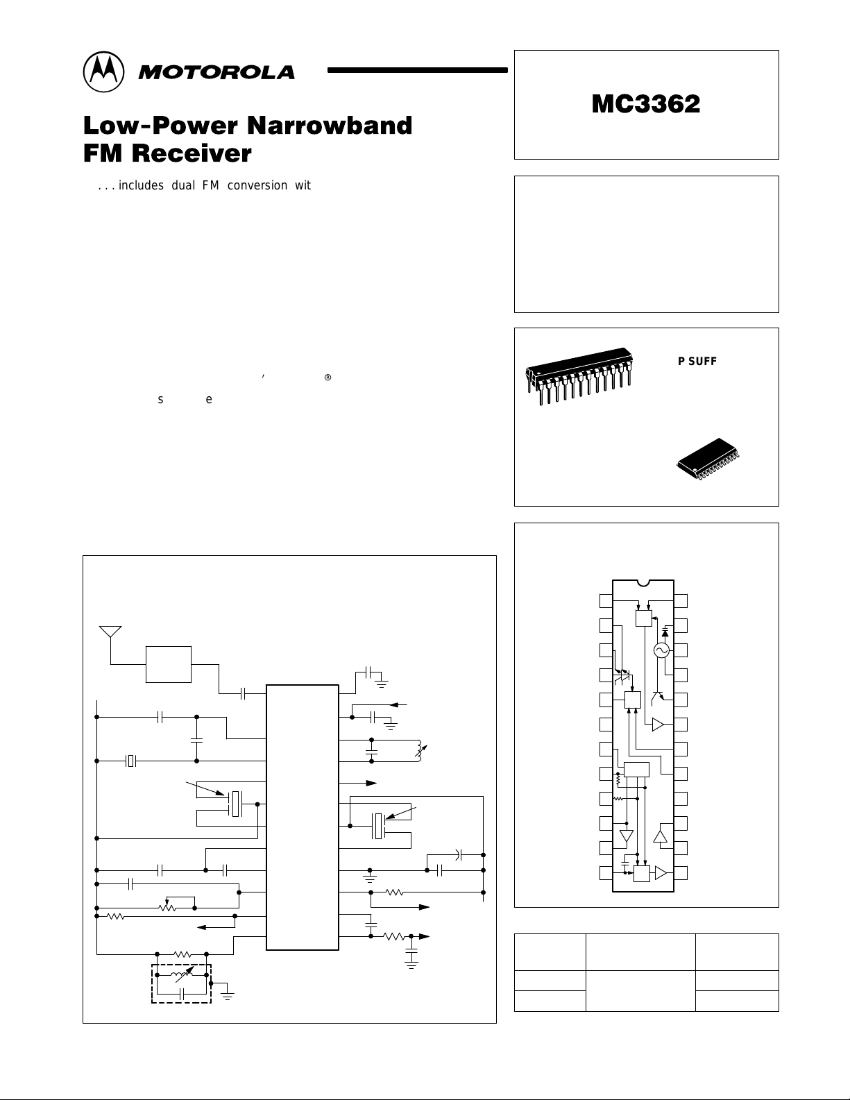
Figure 1. Simplified Application in a PLL Frequency
RF Input
to 200 MHz
V
CC
10.245 MHz
Ceramic Filter
455 kHz
0.1
200 k
To Carrier
10 k
µ
Lp = 680
Cp = 180 pF
H
Input
Match
120 pF
50 pF
0.1
Detect
Indicator
Synthesized Receiver
0.01
1
2
3
4
5
6
0.1
11
39 K
MC3362
24
23
22
21
20
19
187
178
169
1510
14
1312
Figure 2.
From PLL Phase
0.01
To PLL or Prescaler
10 k
0.001
8.2 k
Detector
µ
H
0.41
Ceramic Filter
10.7 MHz
1.0
+
0.1
Data
V
Recovered
Audio
0.01
CC
Figure 2. Pin Connections and
Representative Block Diagram
1st Mixer Input
2nd LO Output
2nd LO Emitter
2nd LO Base
2nd Mixer Output
Limiter Input
Limiter
Decoupling
Limiter
Decoupling
Meter Drive
Carrier Detect
Quadrature Coil
1
X
2
3
4
X
5
6
V
CC
7
8
916
10
11
12
X
ORDERING INFORMATION
Operating
Device
MC3362DW
MC3362P
Temperature Range
TA = – 40 to +85°C
24
1st Mixer Input
23
Varicap Control
22
1st LO Tank
21
1st LO Tank
20
1st LO Output
19
1st Mixer Output
2nd Mixer Input
18
2nd Mixer Input
17
V
EE
15
Comparator Output
14
Comparator Input
13
Detector Output
Package
SO–24L
Plastic DIP
MOTOROLA ANALOG IC DEVICE DATA
Motorola, Inc. 1996 Rev 2
1
Page 2
MC3362
MAXIMUM RATING
Power Supply Voltage (See Figure 2) 6 V
Operating Supply Voltage Range (Recommended) 6 V
Input Voltage (VCC q 5.0 Vdc) 1, 24 V
Junction Temperature – T
Operating Ambient Temperature Range – T
Storage Temperature Range – T
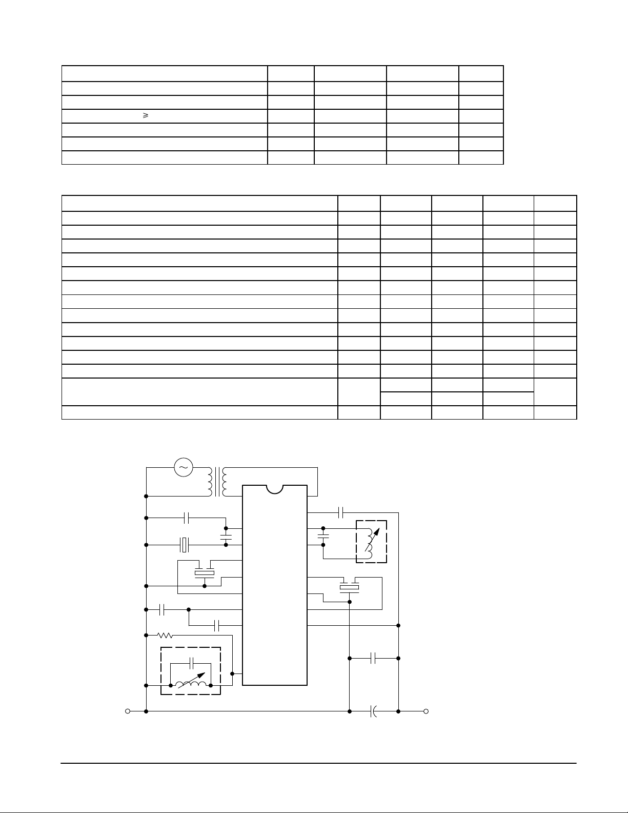
ELECTRICAL CHARACTERISTICS (V
unless otherwise noted)
Drain Current (Carrier Detect Low – See Figure 5) 6 – 4.5 7.0 mA
Input for –3.0 dB Limiting – 0.7 2.0 µVrms
Input for 12 dB SINAD (See Figure 9) – 0.6 – µVrms
Series Equivalent Input Impedence – 450–j350 – Ω
Recovered Audio (RF signal level = 10 mV) 13 – 350 – mVrms
Noise Output (RF signal level = 0 mV) 13 – 250 – mVrms
Carrier Detect Threshold (below VCC) 10 – 0.64 – Vdc
Meter Drive Slope 10 – 100 – nA/dB
Input for 20 dB (S + N)/N (See Figure 7) – 0.7 – µVrms
First Mixer 3rd Order Intercept (Input) – –22 – dBm
First Mixer Input Resistance (Rp) – 690 – Ω
First Mixer Input Capacitance (Cp) – 7.2 – pF
Conversion Voltage Gain, First Mixer – 18 – dB
Conversion Voltage Gain, Second Mixer – 21 –
Dector Output Resistance 13 – 1.4 – kΩ
(TA = 25°C, unless otherwise noted)
Rating
= 5.0 Vdc, fo = 49.7 MHz, Deviation = 3.0 kHz, TA = 25°C, Test Circuit of Figure 3,
CC
Characteristic
Pin Symbol Value Unit
CC(max)
CC
1–24
J
A
stg
Pin Min Typ Max Units
7.0 Vdc
2.0 to 6.0 Vdc
1.0 Vrms
150 °C
– 40 to + 85 °C
– 65 to + 150 °C
RF
Input
10.245
MHz
0.1
Ω
68 k
V
CC
NOTE: See AN980 for Additional Design Information.
T oko RMC–2A6597HM
Ω
50
120 pF
FL1
180 pF
Ferronics
12–345–K
2:6
50 pF
0.1
1
2
3
4
5
6
7
8
9
10
11
Figure 3. T est Circuit
24
23
MC3362
22
21
20
19
18
17
16
15
14
1312
33 pF
FL2
0.01
0.1
1.0
+
µ
F
10.5 Turns
Coilcraft
UNI–10/142
FL1:
muRata CFU455D
Toko LFC–4551
FL2:
muRata SFE10.7MA
T oko SK107M3–A0–10
or
or
V
EE
2
MOTOROLA ANALOG IC DEVICE DATA
Page 3
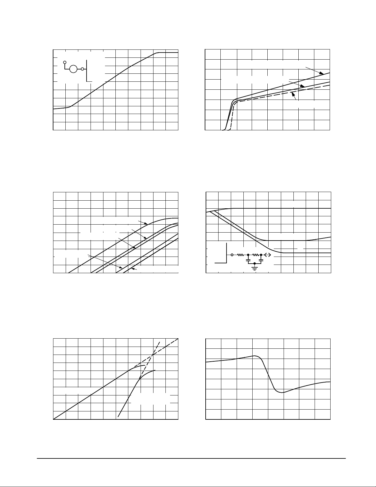
Figure 4. I
12
V
11
CC
10
9.0
8.0
µ
7.0
6.0
10
I ( A)
5.0
4.0
3.0
2.0
– 130 – 110– 120 – 100
10
Meter
MC3362A
RF INPUT (dBm)
versus Input
MC3362
CC
I (mA)
– 30– 40– 50
Figure 5. Drain Current, Recovered Audio
versus Supply
8.0
7.0
6.0
5.0
4.0
3.0
2.0
1.0
0
ICC, Carr. Det. Low (RF in = 10 mV)
ICC, Carr. Det. High (RF in = 0 mV)
5.0
4.0
3.02.00– 90 – 80 – 70 – 60 1.0 6.0 8.0
VCC (V)
Recovered Audio
7.0
800
700
600
500
400
300
200
100
0
13
V (mVrms)
30
20
10
0
– 10
– 20
– 30
– 40
POWER (dBm)
First Mixer Input
– 50
– 60
– 70
– 120 – 110– 130
Figure 6. Signal Levels
Second Mixer Output
First Mixer Output
Second Mixer Input
– 100
– 90 – 80 – 70
RF INPUT (dBm)
RF Input to Transformer
– 40– 50– 60 – 30
– 10
– 20
– 30
– 40
– 50
S + N, N, AMR (dB)
– 60
– 70
– 80
20
10
0
Figure 7. S + N, N, AMR versus Input
S + N
S + N 30% AM
MC3362
13
10 k 10 k
0.010.01
– 1000– 90 – 80 – 70 – 30– 60
RF INPUT (dBm)
Figure 8. 1st Mixer 3rd Order Intermodulation Figure 9. Detector Output versus Frequency
4.0
3.0
2.0
13
V (Vdc)
1.0
– 40
– 20– 30 – 10 0
RELATIVE INPUT FREQUENCY (kHz)
10 20
dB
20
10
– 10
– 20
– 30
– 40
– 50
– 60
– 70
– 80
0
Desired Products
– 90
3rd Order Intermod.
Products
– 80 0– 10
– 70
RF INPUT (dBm)
– 20– 100
– 30– 40– 50– 60 40
N
– 50 – 40– 120 – 1 10– 130
30
MOTOROLA ANALOG IC DEVICE DATA
3
Page 4
MC3362
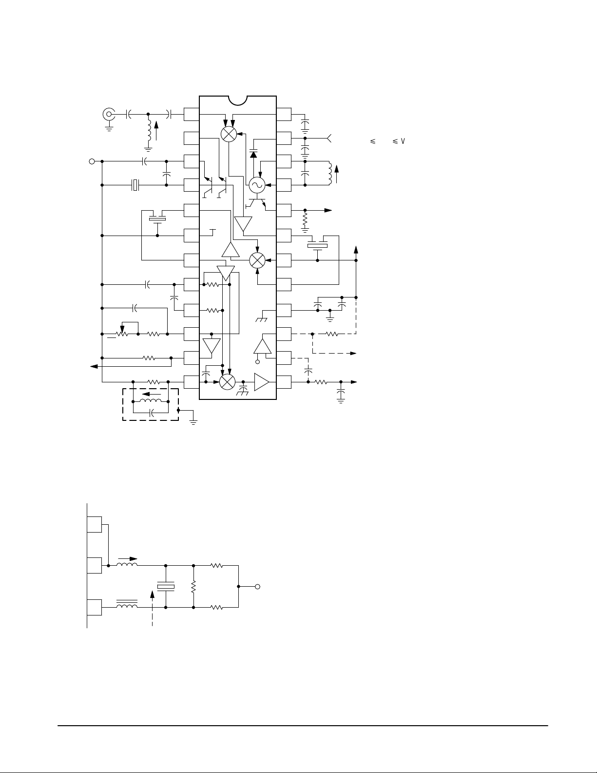
Figure 10. PC Board Test Circuit
(LC Oscillator Configuration Used in PLL Synthesized Receiver)
RF Input
49.67 MHz
Ω
50
VCC = 2.0 to 7.0 Vdc
Carrier
Detect
455 kHz
LC Resonator
18 p
10.245, Fund. Mode
32 pF Load
455 kHz
Cer. Filt.
100 k
Adjust
CD
120 p
0.1
51 k
10 k
39 k
1000 p
0.47
50 p
CRF1
0.10.1
1
µ
2
3
4
5
V
CC
6
7
8
9
10
11
12
(MC3362)
24
23
22
21
20
19
18
17
16
15
+
–
14
13
CRF2
0.01
0.01
33 p
3.0 k
10.7 MHz
Cer. Filt.
10 k
0.001
8.2 k
Varactor Control
(keep 0.7 V
First Local Oscillator
Buffered Output
p
0.41
µ
to V
CC
10.1
FSK Data Output
(optional)
Recovered
Audio
0.01
V23 p VCC)
(This network must be tuned to exactly
10.7 MHz above or below the incoming
RF signal.
NOTE: The IF is rolled off above 10.7
MHz to reduce L.O. feedthrough.)
CRF1 = muRata CFU 455X – the X
suffix denotes 6.0 dB bandwidth.
Rin = R
CRF2 = muRata SFA10.7 MF5 or
SFE10.7 or equivalent. Rin = R
= 330 Ω. Crystal filters can be
used but impedance matching will
need to be added to ensure proper
filter characteristics are realized.
= 1.5 to 2.0 kΩ.
out
out
4
23
22
MC3362
21
Figure 10A. Crystal Oscillator Configuration for Single Channel Application
Crystal used is series mode resonant
(no load capacity specified), 3rd overtone.
This method has not proven adequate for
fundamental mode, 5th or 7th overtone crystals.
The inductor and capacitor will need to be
changed for other frequency crystals. See
AN980 for further information.
0.68
0.68
µ
µ
38.97 MHz
300
20 k
20 k
V
CC
MOTOROLA ANALOG IC DEVICE DATA
Page 5
INPUT Vcc
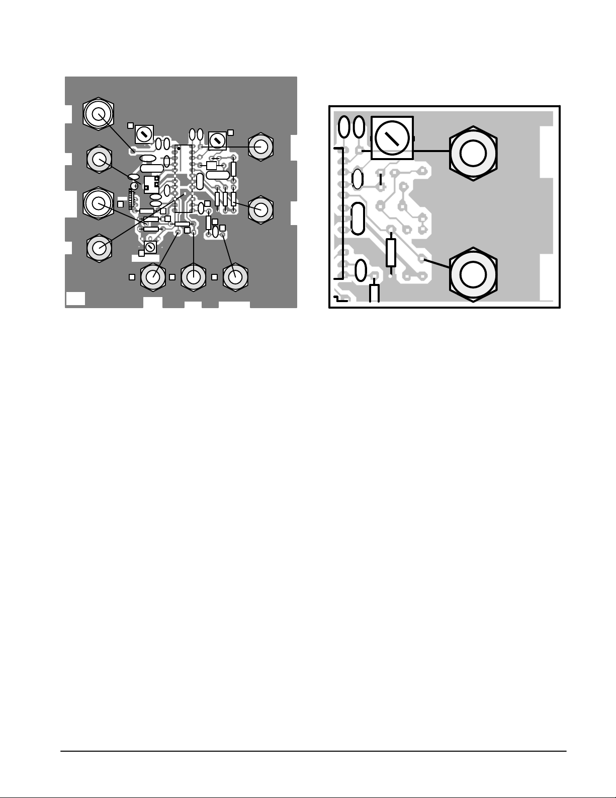
Figure 11. Component Placement V iew
Showing Crystal Oscillator Circuit
MC3362
Figure 11A. LC Oscillator Component View
CARRIER
DETECT
GND
100K
2
8
µ
.47
120p
10.245MHz
.1
1.
51K
4
55VLC06379GT
METER
DRIVE
H
XT
CF
455KHz
10K
68K
TOKO
18p
.1
.1
2
.01
1Kp
50p
MC3362P
.1
2
10K
3
DATA
.01
.68
µ
CF
10.7 MHz
3
.047
H
8.2 K
.68
39 MHz
XT
1
.01
135
7
µ
H
10K
3K
1
REC. AUDIO
330
10K
NOTES: 1. Recovered Audio components may be deleted when using
data output.
2.Carrier Detect components must be deleted in order to obtain
linear Meter Drive output. With these components in place the
Meter Drive outputs serve only to trip the Carrier Detect indicator.
3.Data Output components should be deleted in applications
where only audio modulation is used. For combined audio/data
applications, the 0.047 µF coupling capacitor will add distortion
to the audio, so a pull–down resistor at pin 13 may be required.
4.Use Toko 7MC81282 Quadrature coil.
CONTROLL.O.OUT
.01
33p
CF.047
10.7MHz
.41 µH
3K
.2K
.01
5.Meter Drive cannot be used simultaneously with Carrier Detect output.
For analog meter drive, remove components labelled ″2″and measure
meter current (4–12 µA) through ammeter to VCC.
6.Either type of oscillator circuit may be used with any output circuit
configuration.
7.LC Oscillator Coil: Coilcraft UNI 10/42 10.5 turns, 0.41 µH Crystal
Oscillator circuit: trim coil, 0.68 µH. Coilcraft M1287–A.
8.0.47 H, Coilcraft M1286–A. Input LC network used to match first mixer
input impedance to 50 Ω.
CONTROL
L.O.OUT
CIRCUIT DESCRIPTION
The MC3362 is a complete FM narrowband receiver from
antenna input to audio preamp output. The low voltage dual
conversion design yields low power drain, excellent
sensitivity and good image rejection in narrowband voice and
data link applications.
In the typical application (Figure 1), the first mixer
amplifies the signal and converts the RF input to 10.7 MHz.
This IF signal is filtered externally and fed into the second
mixer, which further amplifies the signal and converts it to a
455 kHz IF signal. After external bandpass filtering, the low IF
is fed into the limiting amplifier and detection circuitry. The
audio is recovered using a conventional quadrature detector.
Twice–IF filtering is provided internally.
The input signal level is monitored by meter drive circuitry
which detects the amount of limiting in the limiting amplifier.
The voltage at the meter drive pin determines the state of the
carrier detect output, which is active low.
APPLICATIONS INFORMATION
The first local oscillator can be run using a free–running
LC tank, as a VCO using PLL synthesis, or driven from an
external crystal oscillator. It has been run to 190 MHz.* A
buffered output is available at Pin 20. The second local
oscillator is a common base Colpitts type which is typically
run at 10.245 MHz under crystal control. A buffered output is
available at Pin 2. Pins 2 and 3 are interchangeable.
The mixers are doubly balanced to reduce spurious
responses. The first and second mixers have conversion
gains of 18 dB and 22 dB (typical), respectively, as seen in
Figure 6. Mixer gain is stable with respect to supply voltage.
For both conversions, the mixer impedances and pin layout
are designed to allow the user to employ low cost, readily
available ceramic filters. Overall sensitivity and AM rejection
are shown in Figure 7. The input level for 20 dB (S + N)/N is
0.7 µV using the two–pole post–detection filter pictured.
*If the first local oscillator (Pins 21 and/or 22) is driven from a
strong external source (100 mVrms), the mixer can be used to
over 450 MHz.
MOTOROLA ANALOG IC DEVICE DATA
5
Page 6
MC3362
Following the first mixer, a 10.7 MHz ceramic band–pass
filter is recommended. The 10.7 MHz filtered signal is then
fed into one second mixer input pin, the other input pin being
connected to VCC. Pin 6 (VCC) is treated as a common point
for emitter–driven signals.
The 455 kHz IF is typically filtered using a ceramic
bandpass filter then fed into the limiter input pin. The limiter
has 10 µV sensitivity for – 3.0 dB limiting, flat to 1.0 MHz.
The output of the limiter is internally connected to the
quadrature detector, including a quadrature capacitor. A
parallel LC tank is needed externally from Pin 12 to VCC. A 39
kΩ shunt resistance is included which determines the peak
separation of the quadrature detector; a smaller value will
increase the spacing and linearity but decrease recovered
audio and sensitivity.
A data shaping circuit is available and can be coupled to
the recovered audio output of Pin 13. The circuit is a
comparator which is designed to detect zero crossings of
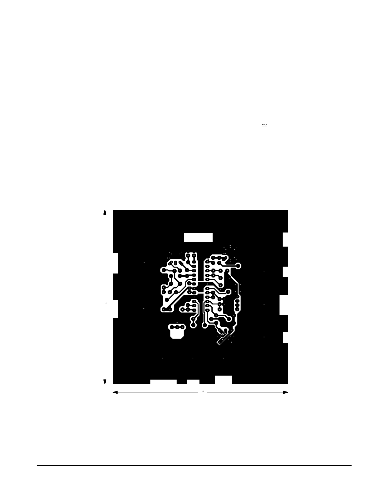
Figure 12. Circuit Side View
FSK modulation. Data rates are typically limited to 1200 baud
to ensure data integrity and avoid adjacent channel “splatter.”
Hysteresis is available by connecting a high valued resistor
from Pin 15 to Pin 14. Values below 120 kΩ are not
recommended as the input signal cannot overcome the
hysteresis.
The meter drive circuitry detects input signal level by
monitoring the limiting amplifier stages. Figure 4 shows the
unloaded current at Pin 10 versus input power. The meter
drive current can be used directly (RSSI) or can be used to
trip the carrier detect circuit at a specified input power. To do
this, pick an RF trip level in dBm. Read the corresponding
current from Figure 4 and pick a resistor such that:
R10 ' 0.64 Vdc / I
10
Hysteresis is available by connecting a high valued resistor
RH between Pins 10 and 1 1. The formula is:
Hysteresis = VCC/(RH x 10 –7) dB
4
I
L.O. OUTCONTROL
REC. AUDIO
MC3362P
DATA
4
I
METER
DRIVE
VCC INPUT
DETECT
CARRIER
GND
6
MOTOROLA ANALOG IC DEVICE DATA
Page 7
MC3362
5
Ω
1.4k
11
15
Ω
400
Ω
400
CC
6V
Ω
100
18
17
4
3
2
12
bias14bias
13
bias
16
V
EE
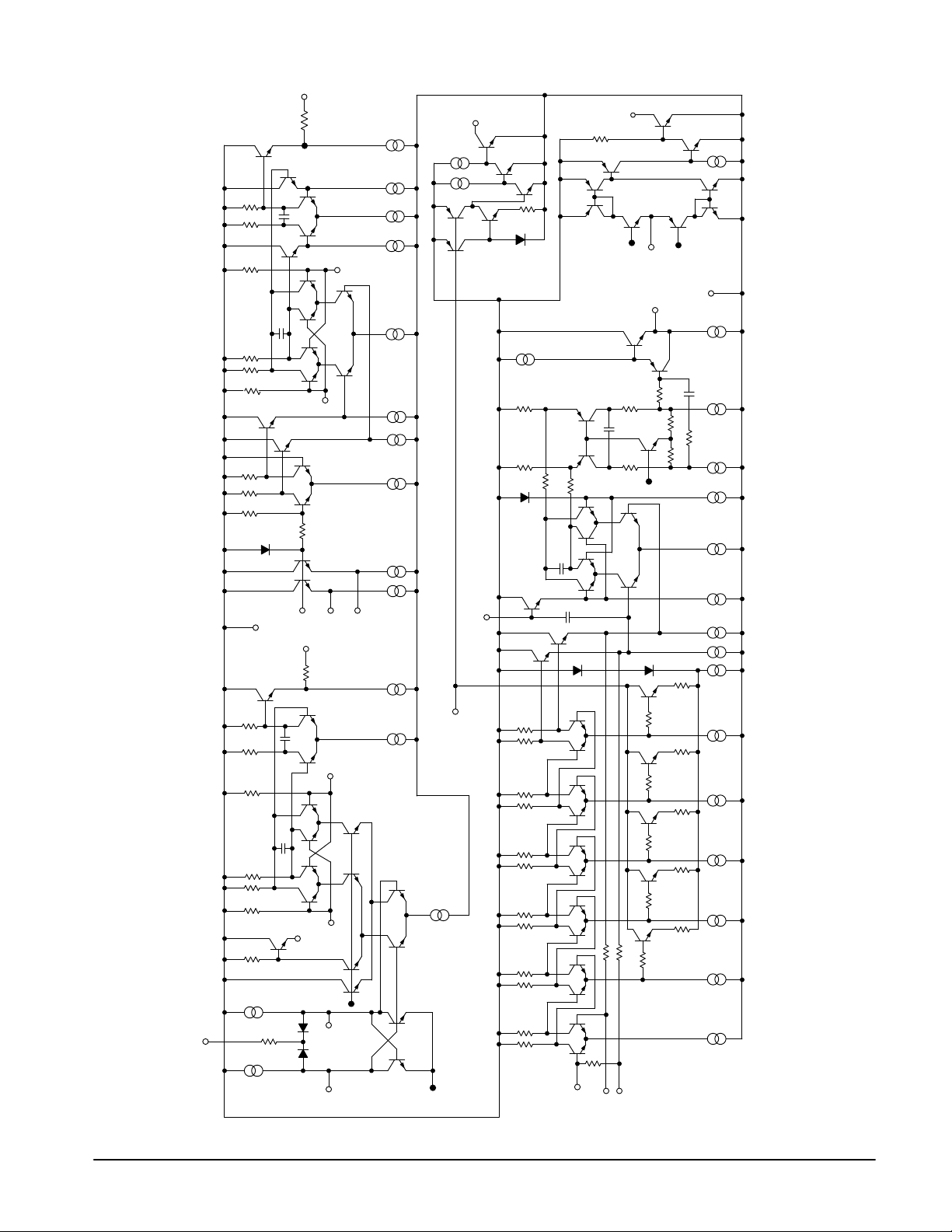
Figure 13. Representative Schematic Diagram
24
Ω
1.0k
Ω
1.0
k
23
20
1
bias
21
MOTOROLA ANALOG IC DEVICE DATA
bias
10
Ω
7
2.0k
8
9
7
Page 8
–T–
SEATING
PLANE
–T–
SEATING
PLANE
–A–
24 13
1
E
G
F
D
–A–
1
D24X
0.010 (0.25) B
M
G22X
–B–
12
N
24 PL
0.25 (0.010) T
S
A
T
MC3362
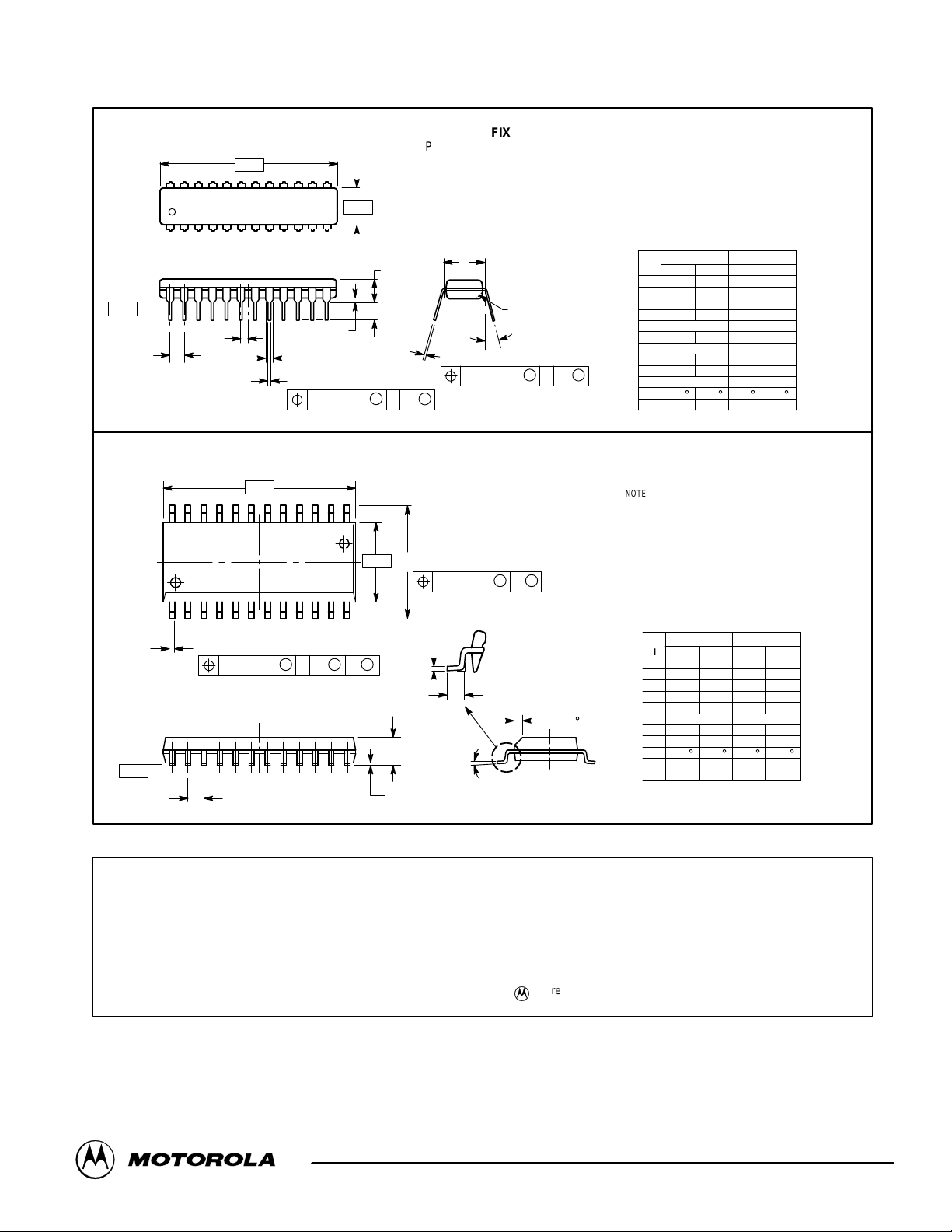
OUTLINE DIMENSIONS
P SUFFIX
PLASTIC PACKAGE
CASE 724–03
ISSUE D
C
K
M
1324
–B– P12X
12
S
A
C
K
L
24 PLJ
0.25 (0.010) T
M
DW SUFFIX
PLASTIC PACKAGE
CASE 751E–04
(SO-24L)
ISSUE E
0.010 (0.25) B
J
F
NOTES:
1. CHAMFERED CONTOUR OPTIONAL.
2. DIMENSION L TO CENTER OF LEADS WHEN
FORMED PARALLEL.
3. DIMENSIONING AND TOLERANCING PER ANSI
Y14.5M, 1982.
4. CONTROLLING DIMENSION: INCH.
DIM MIN MAX MIN MAX
A 1.230 1.265 31.25 32.13
B 0.250 0.270 6.35 6.85
NOTE 1
M
M
M
M
B
M
R
X 45
_
M
C 0.145 0.175 3.69 4.44
D 0.015 0.020 0.38 0.51
E 0.050 BSC 1.27 BSC
F 0.040 0.060 1.02 1.52
G 0.100 BSC 2.54 BSC
J 0.007 0.012 0.18 0.30
K 0.110 0.140 2.80 3.55
L 0.300 BSC 7.62 BSC
M 0 15 0 15
____
N 0.020 0.040 0.51 1.01
NOTES:
1. DIMENSIONING AND TOLERANCING PER ANSI
Y14.5M, 1982.
2. CONTROLLING DIMENSION: MILLIMETER.
3. DIMENSIONS A AND B DO NOT INCLUDE
MOLD PROTRUSION.
4. MAXIMUM MOLD PROTRUSION 0.15 (0.006)
PER SIDE.
5. DIMENSION D DOES NOT INCLUDE DAMBAR
PROTRUSION. ALLOWABLE DAMBAR
PROTRUSION SHALL BE 0.13 (0.005) TOTAL IN
EXCESS OF D DIMENSION AT MAXIMUM
MATERIAL CONDITION.
DIM MIN MAX MIN MAX
A 15.25 15.54 0.601 0.612
B 7.40 7.60 0.292 0.299
C 2.35 2.65 0.093 0.104
D 0.35 0.49 0.014 0.019
F 0.41 0.90 0.016 0.035
G 1.27 BSC 0.050 BSC
J 0.23 0.32 0.009 0.013
K 0.13 0.29 0.005 0.011
M 0 8 0 8
P 10.05 10.55 0.395 0.415
R 0.25 0.75 0.010 0.029
MILLIMETERSINCHES
INCHESMILLIMETERS
____
Motorola reserves the right to make changes without further notice to any products herein. Motorola makes no warranty , representation or guarantee regarding
the suitability of its products for any particular purpose, nor does Motorola assume any liability arising out of the application or use of any product or circuit, and
specifically disclaims any and all liability, including without limitation consequential or incidental damages. “T ypical” parameters which may be provided in Motorola
data sheets and/or specifications can and do vary in different applications and actual performance may vary over time. All operating parameters, including “Typicals”
must be validated for each customer application by customer’s technical experts. Motorola does not convey any license under its patent rights nor the rights of
others. Motorola products are not designed, intended, or authorized for use as components in systems intended for surgical implant into the body, or other
applications intended to support or sustain life, or for any other application in which the failure of the Motorola product could create a situation where personal injury
or death may occur. Should Buyer purchase or use Motorola products for any such unintended or unauthorized application, Buyer shall indemnify and hold Motorola
and its officers, employees, subsidiaries, affiliates, and distributors harmless against all claims, costs, damages, and expenses, and reasonable attorney fees
arising out of, directly or indirectly, any claim of personal injury or death associated with such unintended or unauthorized use, even if such claim alleges that
Motorola was negligent regarding the design or manufacture of the part. Motorola and are registered trademarks of Motorola, Inc. Motorola, Inc. is an Equal
Opportunity/Affirmative Action Employer.
Mfax is a trademark of Motorola, Inc.
How to reach us:
USA/EUROPE/Locations Not Listed: Motorola Literature Distribution; JAPAN: Nippon Motorola Ltd.: SPD, Strategic Planning Office, 4–32–1,
P.O. Box 5405, Denver, Colorado 80217. 303–675–2140 or 1–800–441–2447 Nishi–Gotanda, Shinagawa–ku, Tokyo 141, Japan. 81–3–5487–8488
Mfax: [email protected] – TOUCHTONE 602–244–6609 ASIA/PACIFIC: Motorola Semiconductors H.K. Ltd.; 8B Tai Ping Industrial Park,
– US & Canada ONLY 1–800–774–1848 51 Ting Kok Road, T ai Po, N.T., Hong Kong. 852–26629298
INTERNET: http://motorola.com/sps
8
◊
MOTOROLA ANALOG IC DEVICE DATA
MC3362/D
Page 9

This datasheet has been download from:
www.datasheetcatalog.com
Datasheets for electronics components.
 Loading...