

Page 1
SEMICONDUCTOR
TECHNICAL DATA
HIGH GAIN
LOW POWER
FM IF
Order this document by MC3359/D
P SUFFIX
PLASTIC PACKAGE
CASE 707
DW SUFFIX
PLASTIC PACKAGE
CASE 751D
(SO–20L)
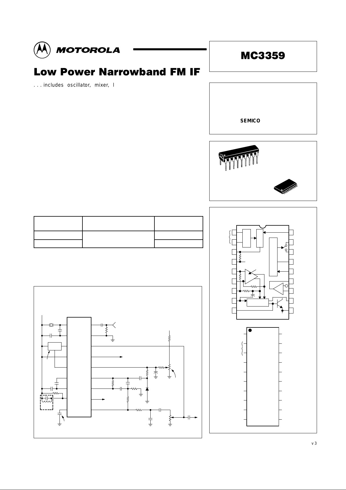
Crystal
Osc.
NC
CASE 707
CASE 751D
50 k
9
–
+
52 k
Limiter
Demodulator
1.8 k
Demod
Output
Recovered
Audio
Filter
Input
Filter
Output
Demodulator
Filter
Decoupling
20
Quadrature
Input
19
18
17
16
15
14
13
12
1110
9
8
7Decoupling
Limiter
Input
V
CC
Mixer
Output
6
1
2
3
4
Crystal
Osc.
Demodulator
Filter
Quadrature
Input
Decoupling
Decoupling
Limiter
Input
V
CC
Mixer
Output
Recovered
Audio
Demod
Output
10
16
15
514
13
12
Audio
Mute
18
NC
10 pF
RF
Input
Scan
Control
Squelch
Input
Filter
Output
Filter
Input
RF
Input
6
7
8
2
3
4
Gnd
1
17
Gnd
Squelch
Input
Audio
Mute
11
5
Scan
Control
Broadcast Detector
Mixer
Oscillator
1.8 k
MC3359DW
Figure 2. Pin Connections and
Functional Block Diagram
1
MOTOROLA ANALOG IC DEVICE DATA
...includes oscillator, mixer, limiting amplifier, AFC, quadrature
discriminator, op/amp, squelch, scan control, and mute switch. The MC3359
is designed to detect narrowband FM signals using a 455 kHz ceramic filter
for use in FM dual conversion communications equipment. The MC3359 is
similar to the MC3357 except that the MC3359 has an additional limiting IF
stage, an AFC output, and an opposite polarity Broadcast Detector. The
MC3359 also requires fewer external parts. For low cost applications
requiring VCC below 6.0 V, the MC3361BP,BD are recommended. For
applications requiring a fixed, tuned, ceramic quadrature resonator, use the
MC3357. For applications requiring dual conversion and RSSI, refer to these
devices; MC3335, MC3362 and MC3363.
• Low Drain Current: 3.6 mA (Typical) @ V
CC
= 6.0 Vdc
• Excellent Sensitivity: Input Limiting Voltage –
– 3.0 dB = 2.0 µV (Typical)
• Low Number of External Parts Required
• For Low Voltage and RSSI, use the MC3371
ORDERING INFORMATION
Device
Operating
Temperature Range
Package
MC3359DW
–
°
SO–20L
MC3359P
T
A
= –30 to +
70°C
Plastic DIP
0.01 µF
Input
VCC = 6.0 Vdc
Audio
Out
Audio
Volume
0.002
µ
F
7.5 k
0.01
µ
F
10 k
Recovered Audio
Automatic
Frequency
Control
390 k
0.001
µ
F
18 k
1N4148
750
0.001
µ
F
0.1
µ
F
120 k
50 k
Squelch
Sensitivity
.47
µ
F
+
68 k
Inverting
Op Amp
(Filter)
Ceramic
Filter
220 pF
V
CC
= 6.0 Vdc
68 pF
MC3359
0.1 µF
0.1 µF
68 k
Quad
Coil
100 pF
0.1
µ
F
51
Mute
Scan Control
Squelch Input
Output
Type
CFU
455 D
51 k
Toko
Type
7MC–8128Z
10.7 MHz
Input
10.245 MHz
910
8
11
712
613
514
415
316
1
18
172
Figure 1. Simplified Application in a Scanner Receiver
Figure 2.
Motorola, Inc. 1996 Rev 3
Page 2
MC3359
2
MOTOROLA ANALOG IC DEVICE DATA
MAXIMUM RATINGS
(TA = 25°C, unless otherwise noted)
Rating
Pin Symbol Value Unit
Power Supply Voltage 4 VCC(max) 12 Vdc
Operating Supply Voltage Range 4 V
CC
6 to 9 Vdc
Input Voltage (VCCq
6.0 Volts) 18 V
18
1.0 V
rms
Mute Function 16 V
16
– 0.7 to 12 V
pk
Junction Temperature – T
J
150 °C
Operating Ambient Temperature Range – T
A
– 30 to + 70 °C
Storage Temperature Range – T
stg
– 65 to + 150 °C
ELECTRICAL CHARACTERISTICS (V
CC
= 6.0 Vdc, fo = 10.7 MHz, ∆f = ± 3.0 kHz, f
mod
= 1.0 kHz, 50 Ω source, TA = 25°C test circuit
of Figure 3, unless otherwise noted)
Characteristics
Min Typ Max Units
Drain Current (Pins 4 and 8) Squelch Off
Squelch On
–
–
3.6
5.4
6.0
7.0
mA
Input for 20 dB Quieting – 8.0 – µVrms
Input for – 3.0 dB Limiting – 2.0 – µVrms
Mixer Voltage Gain (Pin 18 to Pin 3, Open) – 46 –
Mixer Third Order Intercept, 50 Ω Input – – 1.0 – dBm
Mixer Input Resistance – 3.6 – kΩ
Mixer Input Capacitance – 2.2 – pF
Recovered Audio, Pin 10
(Input Signal 1.0 mVrms)
450 700 – mVrms
Detector Center Frequency Slope, Pin 10 – 0.3 – V/kHz
AFC Center Slope, Pin 11, Unloaded – 12 – V/kHz
Filter Gain (test circuit of Figure 3) 40 51 – dB
Squelch Threshold, Through 10K to Pin 14 – 0.62 – Vdc
Scan Control Current, Pin 15 Pin 14 – High
–
0.01
1.0 µA
g
Pin 14 – Low 2.0 2.4 –
µ
mA
Mute Switch Impedance
Pin 14 – High
– 5.0
10 Ω
p
Pin 16 to Ground
g
Pin 14 – Low 1.5 – MΩ
0.1 µF
Op Amp Output
Audio Gen.
0.7 Vp–p
Squelch Input
10 k
AFC Output
Op Amp Input
10.245 MHz
V
CC
68
pF
220 pF
Audio Output
1
17
2.4 k
2
muRata
CFU455D
or
Kyocera
KBF455P–20A
3
7.5 k
4
I
+
1.0 M
1.0 k
1.0
µ
F
0.002
µ
F
15
14
13
12
11
18
Ceramic
Filter
10
16
9
Lp = 1.0 mH
Cp = 120 pF
Rp = 100 k
Ω
8
0.1
µ
F
7
100 pF
6
68 k
5
0.1
µ
F
Input
10.7 MHz
51
Figure 3. Test Circuit
Page 3
MC3359
3
MOTOROLA ANALOG IC DEVICE DATA
– 2.0– 4.0– 6.0– 8.0 4.0 6.0 8.0
4.0
6.0
10
20
40
60
100
200
400
100101.00.1
– 70
– 60
– 50
– 40
– 10
– 30
– 20
0
FREQUENCY [MHz]
10
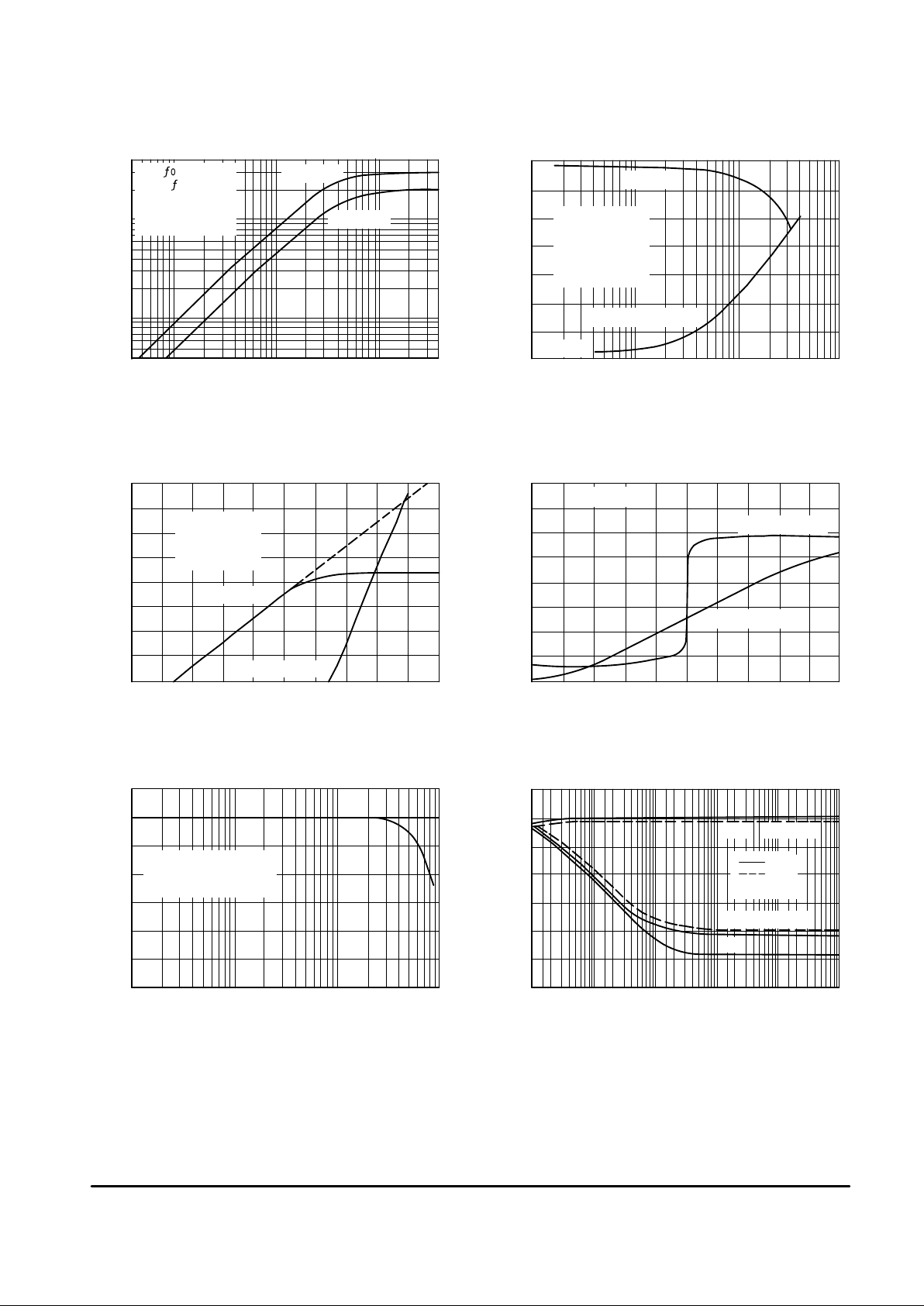
Figure 4. Mixer Voltage Gain
INPUT, 50 Ω (mVrms)
75
°
C
25
°
C
VCC = 6.0 Vdc
10010
5.0
–90 –80
– 20
– 10
10
10
0
0.1
20
0
10
–70 –60 –50 –40
– 40
4.0
0.1 1.0
– 20
–30
– 30
– 40
– 50
– 60
0.001
INPUT [mVrms]
1.00.01
400.1 1.00.04
– 30
10
–20 –10
3.0
010
–10
–20
–40
–50
2.0
1.0
0
– 10
RELATIVE FREQUENCY [kHz]
FREQUENCY [MHz]
100
2.00
0
–60
10
– 60
8.0
– 50
7.0
6.0
INPUT, 50
Ω
[dBm]
– 10
RELATIVE GAIN [dB]
RELATIVE OUTPUT [dB] OUTPUT [Vdc]
RELATIVE OUTPUT [dB]
OUTPUT, 1.8 K [dBm]
–30
INPUT LEVEL, 50 [dBm]
Ω
Ω
OUTPUT, 1.8 K [mVrms]
Ω
Input po = 10.7 MHz
Output
p
0 = 455 kHz
Output taken at
Pin 3 with filter
removed (open)
VCC = 9.0 V
VCC = 6.0 V
Figure 5. Limiting IF Frequency Response
100 µV
Response Taken on
a special prototype.
Terminals not
available on
standard device.
IF Output
IF Input for –3 dB LImiting
Figure 6. Mixer Third Order
Intermodulation Performance
Output taken at
Pin 3 with filter
removed
VCC = 6.0 Vdc
Desired Products
3rd Order IM Products
Figure 7. Detector and AFC Responses
VCC = 6.0 Vdc
AFC Output Pin 11
Detector Output Pin 10
Derived using optimum L/C
oscillator values and holding
IF frequency at 455 kHz
Figure 8. Relative Mixer Gain Figure 9. Overall Gain, Noise, and AM Rejection
S+N±3 KHz FM
S + N (30% AM)
N
Page 4

MC3359
4
MOTOROLA ANALOG IC DEVICE DATA
INPUT [mVrms]
120
150
180
FREQUENCY [kHz]
10050205.0 102.01.0
0
0.2
0.4
0.6
10
20
30
50
70
100
200
300
500
700
0.1
0.2
0.3
0.5
0.7
1.0
7050302010
1000
7.0 100
OSCILLAT OR FREQUENCY [MHz]
100 K 1.0 M 10 M
FREQUENCY [Hz]
70
0
–50
–40
–30
60
–20
–10
0
10
0
0.1
0.5
0.6
0.7
0.8
5.9
9.08.07.05.0
10 K
6.04.0
0
5040
1.0
2.0
3.0
4.0
5.0
7.0
6.0
8.0
VCC, SUPPLY VOLTAGE (Vdc)
Figure 10. Output Components of Signal,
Noise, and Distortion
0.2
0.3
0.4
0
1.0 K
AMBIENT TEMPERATURE [
°
C]
20 30
5.0
101.00.10.010.001
6.0
VCC, SUPPLY VOLTAGE [Vdc]
6.1 6.2
10.706
10.704
10.702
10.700
10.698
10.696
10.694
10.690
10.692
70
60
50
40
30
20
10
90
60
30
100
–60
5.8
RELATIVE OUTPUT [dB]
SUPPLY CURRENT (mAdc)
AUDIO OUTPUT (Vrms)
GAIN [dB]
PHASE [degrees]
FREQUENCY [MHz]
CAPACITANCE [pF]
INDUCT ANCE [ H]
OUTPUT [Vrms]
µ
S + N + D
N + D
N
f
o = 10.7 MHz
f
m = 1 kHz
∆
f = "3.0 kHz
Test circuit of
Figure 3.
Audio Output
ICC, Mute On
ICC, Mute Off
Figure 11. Audio Output and Total Current
Drain versus Supply Voltage
Figure 12. L/C Oscillator, Temperature and
Power Supply Sensitivity
V
CC
Temp
Phase
Gain
USE CIRCUIT ABOVE
FOR OPEN LOOP GAIN
AND PHASE (SOLID LINES)
13
12
1.0 K
1.0 M
0.1
µ
F
V
ref
1.0 M
1.0
DOTTED CURVES TAKEN
WITH CIRCUIT VALUES
OF FIGURE 3.
VCC = 6.0 Vdc
L
C
5
C
4
C
5
C
4
L
V
CC
2
1
10
7.0
5.0
4.0
3.0
2.0
1.0
0.8
GIVEN
f
o
= CENTER FREQUENCY
A(
f
o
) = GAIN AT CENTER FREQUENCY
R3
+
Q
p
foC1
R1
+
R3
2A(f
o
)
R2
+
R1 R3
4Q
2
R1*R3
R1
18 K
0.001
µ
F
V
out
V
in
0.17
Vrms
R3
390 K
V
ref
C1
12
V
CC
6.0 V
13
C1
0.001
µ
F
R2
750
+
–
Figure 13. Op Amp Gain and Phase Response
Figure 14. L/C Oscillator Recommended
Component Values
Figure 15. The Op Amp as a Bandpass Filter
Page 5

MC3359
5
MOTOROLA ANALOG IC DEVICE DATA
17
7
5
10 k 33k 33k 33 k 33 k 33 k 10k
50 k
100 k 10k 10 k 10 k 10 k 10 k 10 k 10 k 10k 10 k 10 k 10 k 10 k
10
k
33 k 5 k
1.6 k
1.6 k
1.6 k
1.6 k
100 k
9
10
11
1.6 k
1.6 k
1.6 k
1.6 k
1.6 k
1.6 k
100 k
33 k
10 pF
50 k7 k 50 k 2.5 k
750
Ω
5k
50 k
5k20 k
50 k 20 k
3.5 k
100 k
1.8 k
15 k
4
16
15
1413123
10 k
33 k33 k3.5 k
20 k
33 k33 k33 k
7k7k
5k
3.6 k
6pF 6pF
15 k
18
2
1
Q77
Q1
Q2
Q3 Q4 Q5 Q6
Q9
Q8
Q10
Q11
Q12
Q13
Q14
Q15 Q16
Q7
Q60
Q64
Q66
Q65
Q71
Q61
Q62
Q68
Q69
Q70
Q63
Q67
Q71
Q76
Q75
Q73
Q59
Q50
Q56
Q58
Q55
Q47
Q49
Q51
Q54
Q53
Q57
Q52
Q44Q43
Q42Q41
Q40
Q39
Q37
Q36
Q35
Q34
Q33
Q32
Q31
Q30
Q29
Q28
Q27
Q26
Q25
Q24Q23
1.8 k
Q21
Q20
Q19
Q18
Q17
Q22
6
Figure 16.
Figure 16. Representative Schematic Diagram
Oscillator – Mixer
Limiting IF Amplifier
Op Amp
Detector and AFC
Broadcast Detector
Q45 Q48
Q46
Page 6

MC3359
6
MOTOROLA ANALOG IC DEVICE DATA
CIRCUIT DESCRIPTION
The MC3359 is a low–power FM IF circuit designed
primarily for use in voice–communication scanning receivers.
It is also finding a place in narrowband data links.
In the typical application (Figure 1), the mixer–oscillator
combination converts the input frequency (10.7 MHz) down
to 455 kHz, where, after external bandpass filtering, most of
the amplification is done. The audio is recovered using a
conventional quadrature FM detector. The absence of an
input signal is indicated by the presence of noise above the
desired audio frequencies. This “noise band” is monitored by
an active filter and a detector. A squelch–trigger circuit
indicates the presence of noise (or a tone) by an output which
can be used to control scanning. At the same time, an
internal switch is operated which can be used to mute the
audio.
APPLICATIONS INFORMATION
The oscillator is an internally biased Colpitts type with the
collector, base, and emitter connections at Pin 4, 1 and 2,
respectively. The crystal is used in fundamental mode,
calibrated for parallel resonance at 32 pF load capacitance.
In theory this means that the two capacitors in series should
be 32 pF, but in fact much larger values do not significantly
affect the oscillator frequency, and provide higher oscillator
output.
The oscillator can also be used in the conventional L/C
Colpitts configuration without loss of mixer conversion gain.
This oscillator is, of course, much more sensitive to voltage
and temperature as shown in Figure 12. Guidelines for
choosing L and C values are given in Figure 14.
The mixer is doubly balanced to reduce spurious
responses. The mixer measurements of Figure 4 and 6 were
made using an external 50 Ω source and the internal 1.8 k at
Pin 3. Voltage gain curves at several VCC voltages are shown
in Figure 4. The Third Order Intercept curves of Figure 6 are
shown using the conventional dBm scales. Measured power
gain (with the 50 Ω input) is approximately 18 dB but the
useful gain is much higher because the mixer input
impedance is over 3 kΩ. Most applications will use a 330 Ω
10.7 MHz crystal filter ahead of the mixer. For higher
frequencies, the relative mixer gain is given in Figure 8.
Following the mixer, a ceramic bandpass filter is
recommended. The 455 kHz types come in bandwidths from
±2 kHz to ± 15 kHz and have input and output impedances of
1.5 k to 2.0 k. For this reason, the Pin 5 input to the 6 stage
limiting IF has an internal 1.8 k resistor. The IF has a 3 dB
limiting sensitivity of approximately 100 µV at Pin 5 and a
useful frequency range of about 5 MHz as shown in Figure 5.
The frequency limitation is due to the high resistance values
in the IF, which were necessary to meet the low power
requirement. The output of the limiter is internally connected
to the quadrature detector, including the 10 pF quadrature
capacitor. Only a parallel L/C is needed externally from Pin 8
to VCC. A shunt resistance can be added to widen the peak
separation of the quadrature detector.
The detector output is amplified and buffered to the audio
output, Pin 10, which has an output impedance of
approximately 300 Ω. Pin 9 provides a high impedance (50 k)
point in the output amplifier for application of a filter or
de–emphasis capacitor. Pin 11 is the AFC output, with high
gain and high output impedance (1 M). If not needed, it
should be grounded, or it can be connected to Pin 9 to double
the recovered audio. The detector and AFC responses are
shown in Figure 7.
Overall performance of the MC3359 from mixer input to
audio output is shown in Figure 9 and 10. The MC3359 can
also be operated in “single conversion” equipment; i.e., the
mixer can be used as a 455 kHz amplifier. The oscillator is
disabled by connecting Pin 1 to Pin 2. In this mode, the
overall performance is identical to the 10.7 MHz results of
Figure 9.
A simple inverting op amp is provided with an output at
Pin 13 providing dc bias (externally) to the input at Pin 12,
which is referred internally to 2.0 V. A filter can be made with
external impedance elements to discriminate between
frequencies. With an external AM detector, the filtered audio
signal can be checked for the presence of either noise above
the normal audio, or a tone signal.
The open loop response of this op amp is given in
Figure13. Bandpass filter design information is provided in
Figure 15.
A low bias to Pin 14 sets up the squelch–trigger circuit so
that Pin 15 is high, a source of at least 2.0 mA, and the audio
mute (Pin 16) is open–circuit. If Pin 14 is raised to 0.7 V by
the noise or tone detector, Pin 15 becomes open circuit and
Pin 16 is internally short circuited to ground. There is no
hysteresis. Audio muting is accomplished by connecting Pin
16 to a high–impedance ground–reference point in the audio
path between Pin 10 and the audio amplifier. No dc voltage is
needed, in fact it is not desirable because audio “thump”
would result during the muting function. Signal swing greater
than 0.7 V below ground on Pin 16 should be avoided.
Page 7

MC3359
7
MOTOROLA ANALOG IC DEVICE DATA
OUTLINE DIMENSIONS
NOTES:
1. POSITIONAL TOLERANCE OF LEADS (D),
SHALL BE WITHIN 0.25 (0.010) AT MAXIMUM
MATERIAL CONDITION, IN RELATION TO
SEATING PLANE AND EACH OTHER.
2. DIMENSION L TO CENTER OF LEADS WHEN
FORMED PARALLEL.
3. DIMENSION B DOES NOT INCLUDE MOLD
FLASH.
1
SEATING
PLANE
10
9
18
M
A
B
K
C
N
F
G
D
H
J
L
DIM MIN MAX MIN MAX
INCHESMILLIMETERS
A 22.22 23.24 0.875 0.915
B 6.10 6.60 0.240 0.260
C 3.56 4.57 0.140 0.180
D 0.36 0.56 0.014 0.022
F 1.27 1.78 0.050 0.070
G 2.54 BSC 0.100 BSC
H 1.02 1.52 0.040 0.060
J 0.20 0.30 0.008 0.012
K 2.92 3.43 0.115 0.135
L 7.62 BSC 0.300 BSC
M 0 15 0 15
N 0.51 1.02 0.020 0.040
__ __
NOTES:
1. DIMENSIONING AND TOLERANCING PER
ANSI Y14.5M, 1982.
2. CONTROLLING DIMENSION: MILLIMETER.
3. DIMENSIONS A AND B DO NOT INCLUDE
MOLD PROTRUSION.
4. MAXIMUM MOLD PROTRUSION 0.150
(0.006) PER SIDE.
5. DIMENSION D DOES NOT INCLUDE
DAMBAR PROTRUSION. ALLOWABLE
DAMBAR PROTRUSION SHALL BE 0.13
(0.005) TOTAL IN EXCESS OF D DIMENSION
AT MAXIMUM MATERIAL CONDITION.
–A–
–B–
20
1
11
10
S
A
M
0.010 (0.25) B
S
T
D20X
M
B
M
0.010 (0.25)
P10X
J
F
G
18X
K
C
–T–
SEATING
PLANE
M
R
X 45
_
DIM MIN MAX MIN MAX
INCHESMILLIMETERS
A 12.65 12.95 0.499 0.510
B 7.40 7.60 0.292 0.299
C 2.35 2.65 0.093 0.104
D 0.35 0.49 0.014 0.019
F 0.50 0.90 0.020 0.035
G 1.27 BSC 0.050 BSC
J 0.25 0.32 0.010 0.012
K 0.10 0.25 0.004 0.009
M 0 7 0 7
P 10.05 10.55 0.395 0.415
R 0.25 0.75 0.010 0.029
__
__
P SUFFIX
PLASTIC PACKAGE
CASE 707–02
ISSUE C
DW SUFFIX
PLASTIC PACKAGE
CASE 751D–04
(SO–20L)
ISSUE E
Page 8

MC3359
8
MOTOROLA ANALOG IC DEVICE DATA
Motorola reserves the right to make changes without further notice to any products herein. Motorola makes no warranty , representation or guarantee regarding
the suitability of its products for any particular purpose, nor does Motorola assume any liability arising out of the application or use of any product or circuit, and
specifically disclaims any and all liability, including without limitation consequential or incidental damages. “T ypical” parameters which may be provided in Motorola
data sheets and/or specifications can and do vary in different applications and actual performance may vary over time. All operating parameters, including “Typicals”
must be validated for each customer application by customer’s technical experts. Motorola does not convey any license under its patent rights nor the rights of
others. Motorola products are not designed, intended, or authorized for use as components in systems intended for surgical implant into the body, or other
applications intended to support or sustain life, or for any other application in which the failure of the Motorola product could create a situation where personal injury
or death may occur. Should Buyer purchase or use Motorola products for any such unintended or unauthorized application, Buyer shall indemnify and hold Motorola
and its officers, employees, subsidiaries, affiliates, and distributors harmless against all claims, costs, damages, and expenses, and reasonable attorney fees
arising out of, directly or indirectly, any claim of personal injury or death associated with such unintended or unauthorized use, even if such claim alleges that
Motorola was negligent regarding the design or manufacture of the part. Motorola and are registered trademarks of Motorola, Inc. Motorola, Inc. is an Equal
Opportunity/Affirmative Action Employer.
How to reach us:
USA/EUROPE/Locations Not Listed: Motorola Literature Distribution; JAPAN: Nippon Motorola Ltd.; Tatsumi–SPD–JLDC, 6F Seibu–Butsuryu–Center,
P.O. Box 20912; Phoenix, Arizona 85036. 1–800–441–2447 or 602–303–5454 3–14–2 Tatsumi Koto–Ku, Tokyo 135, Japan. 03–81–3521–8315
MFAX: RMF AX0@email.sps.mot.com – TOUCHT ONE 602–244–6609 ASIA/PACIFIC: Motorola Semiconductors H.K. Ltd.; 8B Tai Ping Industrial Park,
INTERNET: http://Design–NET .com 51 Ting Ko k Road, Tai Po, N.T., Hong Kong. 852–26629298
MC3359/D
*MC3359/D*
◊
 Loading...