

Page 1
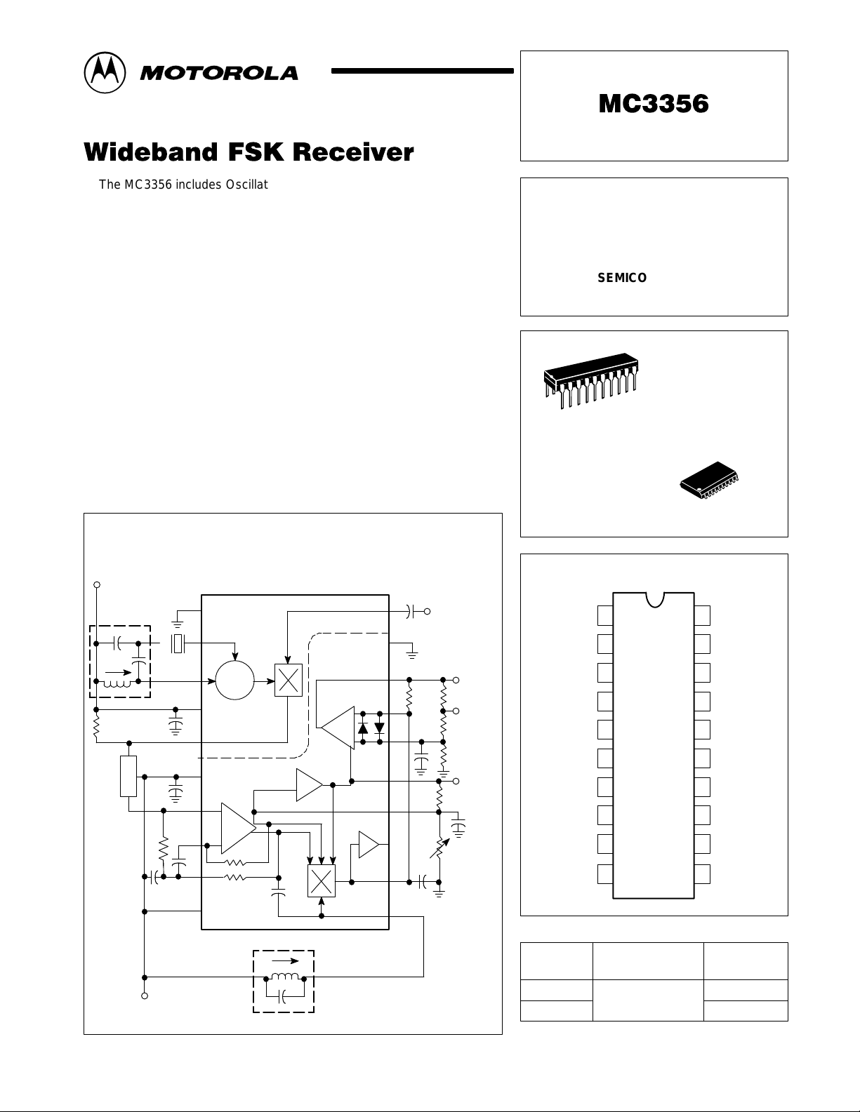
The MC3356 includes Oscillator, Mixer, Limiting IF Amplifier, Quadrature
Detector, Audio Buffer, Squelch, Meter Drive, Squelch Status output, and
Data Shaper comparator. The MC3356 is designed for use in digital data
communciations equipment.
• Data Rates up to 500 kilobaud
• Excellent Sensitivity: – 3 dB Limiting Sensitivity
Excellent Sensitivity: 30 µVrms @ 100 MHz
• Highly Versatile, Full Function Device, yet Few External Parts are
Required
• Down Converter Can be Used Independently — Similar to NE602
Order this document by MC3356/D
WIDEBAND
FSK
RECEIVER
SEMICONDUCTOR
TECHNICAL DATA
P SUFFIX
PLASTIC PACKAGE
CASE 738
RF
V
CC
Ceramic
Filter
Figure 1. Representative Block Diagram
RF
Ground
1
2
3
OSC
4
5
6
7
8
9
Mixer
Comparator
Meter Current
Limiter
Data Shaping
Comparator
+
–
–
+
Buffer
20
19
18
17
16
15
14
13
12
RF
Input
Ground
Data
Output
V
CC
Squelch
Status
Hysteresis
Squelch
Adjust
(Meter)
DW SUFFIX
PLASTIC PACKAGE
CASE 751D
(SO–20L)
PIN CONNECTIONS
RF Ground
IF V
CC
CC
2
3
4
5
6
7
8
9
10
OSC Emitter
OSC Collector
RF V
Mixer Output
Limiter Input
Limiter Bias
Limiter Bias
Quad Bias
201
RF Input
19
Ground
18
Data Output
17
+ Comparator
16
– Comparator
15
Squelch Status
14
Squelch Control
Buffered Output
13
Demodulator
12
Filter
11
Quad Input
10
Quadrature Detector
V
CC
MOTOROLA ANALOG IC DEVICE DATA
Tank
11
ORDERING INFORMATION
Operating
Device
MC3356DW
MC3356P
Motorola, Inc. 1996 Rev 0
Temperature Range
TA = – 40 to +85°C
Package
SO–20L
Plastic DIP
1
Page 2
MAXIMUM RATINGS
Rating Symbol Value Unit
Power Supply Voltage V
Operating Power Supply Voltage Range (Pins 6, 10) V
Operating RF Supply Voltage Range (Pin 4) RF V
Junction Temperature T
Operating Ambient Temperature Range T
Storage Temperature Range T
Power Dissipation, Package Rating P
MC3356
CC(max)
CC
CC
J
A
stg
D
15 Vdc
3.0 to 9.0 Vdc
3.0 to 12.0 Vdc
150 °C
– 40 to + 85 °C
– 65 to + 150 °C
1.25 W
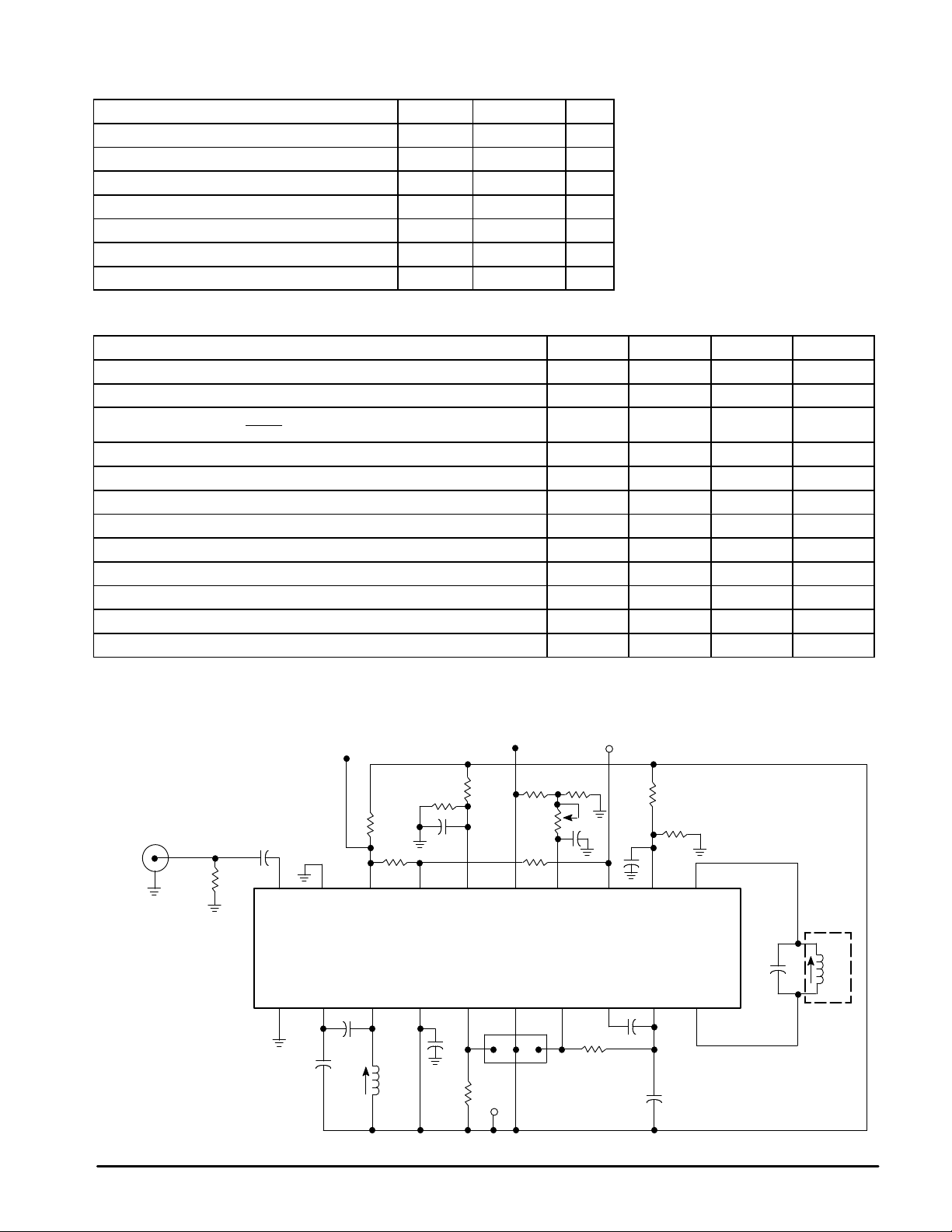
ELECTRICAL CHARACTERISTICS (V
= 5.0 Vdc, fo = 100 MHz, f
CC
= 110.7 MHz, ∆f = ±75 kHz, f
osc
= 1.0 kHz, 50 Ω source,
mod
TA = 25°C, test circuit of Figure 2, unless otherwise noted.)
Characteristics
Drain Current Total, RF VCC and V
CC
Min Typ Max Unit
– 20 25 mAdc
Input for – 3 dB limiting – 30 – µVrms
Input for 50 dB quieting
S + N
()
N
– 60 – µVrms
Mixer Voltage Gain, Pin 20 to Pin 5 2.5 – –
Mixer Input Resistance, 100 MHz – 260 – Ω
Mixer Input Capacitance, 100 MHz – 5.0 – pF
Mixer/Oscillator Frequency Range (Note 1) – 0.2 to 150 – MHz
IF/Quadrature Detector Frequency Range (Note 1) – 0.2 to 50 – MHz
AM Rejection (30% AM, RF Vin = 1.0 mVrms) – 50 – dB
Demodulator Output, Pin 13 – 0.5 – Vrms
Meter Drive – 7.0 – µA/dB
Squelch Threshold – 0.8 – Vdc
NOTE: 1. Not taken in Test Circuit of Figure 2; new component values required.
Figure 2. T est Circuit
Data Output
Squelch
Status
Demod
Out
100 MHz
RF Input
L1 – 110.7 MHz, 0.4 µH
L1 – 7T #22, 3/16 Form
L1 – w/slug & can
L2 – 10.7 MHz, 1.5 µH
L2 – 20T #30, 3/16 Form
L2 – w/slug & can
T1 – muRata
T1 – SFE10.7 MA5–Z
or KYOCERA
T1 – KBF10.7MN–MA
2
CC
5 Vdc
130 k 3.3 k
3.0 k
3.3 k
Status
V
CC
T1V
Squelch
Control
Limiter
Input
0.1
330
470
Demod
Out
Limiter
Bias
pF
0.01
18 k
Demod
Filter
Limiter
Bias
0.01
18 k
Quad
Input
Quad
Bias
47 k
47 k
10 k
0.01
51 20 19 18 17 16 15 14 13 12 11
RF Input Ground Data
RF
OSC
Gnd
EM.
5.6 pF
15 pF
390 k
Output
OSC
COL.RFV
L1
0.01
Comp(+) Comp(–) Squelch
Mixer
Out
CC
0.01
330
MOTOROLA ANALOG IC DEVICE DATA
150 pF
10987654321
L2
Page 3
Figure 3. Output Components of Signal,
Noise, and Distortion
10
0
–10
–20
S + N + D
fO = 100 MHz
fm = 1.0 kHz
∆
f = ± 75 kHz
MC3356
Figure 4. Meter Current versus Signal Input
700
600
µ
500
400
–30
–40
RELATIVE OUTPUT (dB)
–50
–60
0.01 0.1 1.0 10
N + D
N
INPUT (mVrms)
GENERAL DESCRIPTION
This device is intended for single and double conversion
VHF receiver systems, primarily for FSK data transmission
up to 500 K baud (250 kHz). It contains an oscillator, mixer,
limiting IF, quadrature detector, signal strength meter drive,
and data shaping amplifier.
The oscillator is a common base Colpitts type which can
be crystal controlled, as shown in Figure 1, or L–C controlled
as shown in the other figures. At higher VCC, it has been
operated as high as 200 MHz. A mixer/oscillator voltage gain
of 2 up to approximately 150 MHz, is readily achievable.
The mixer functions well from an input signal of
10 µVrms, below which the squelch is unpredictable, up to
about 10 mVrms, before any evidence of overload.
Operation up to 1.0 Vrms input is permitted, but non–linearity
of the meter output is incurred, and some oscillator pulling is
suspected. The AM rejection above 10 mVrms is degraded.
The limiting IF is a high frequency type, capable of being
operated up to 50 MHz. It is expected to be used at 10.7 MHz
in most cases, due to the availability of standard ceramic
resonators. The quadrature detector is internally coupled to
the IF, and a 5.0 pF quadrature capacitor is internally
provided. The –3dB limiting sensitivity of the IF itself is
approximately 50 µV (at Pin 7), and the IF can accept signals
up to 1.0 Vrms without distortion or change of detector
quiescent dc level.
The IF is unusual in that each of the last 5 stages of the
6 state limiter contains a signal strength sensitive, current
sinking device. These are parallel connected and buffered to
produce a signal strength meter drive which is fairly linear for
IF input signals of 10 µV to 100 mVrms (see Figure 4).
A simple squelch arrangement is provided whereby the
meter current flowing through the meter load resistance flips
a comparator at about 0.8 Vdc above ground. The signal
strength at which this occurs can be adjusted by changing
the meter load resistor. The comparator (+) input and output
are available to permit control of hysteresis. Good positive
300
200
100
METER CURRENT, PIN 14 ( A)
0
0.010 0.1 1.0 10 100 1000
PIN 20 INPUT (mVrms)
action can be obtained for IF input signals of above 30
µVrms. The 130 kΩ resistor shown in the test circuit provides
a small amount of hysteresis. Its connection between the
3.3 k resistor to ground and the 3.0 k pot, permits adjustment
of squelch level without changing the amount of hysteresis.
The squelch is internally connected to both the
quadrature detector and the data shaper. The quadrature
detector output, when squelched, goes to a dc level
approximately equal to the zero signal level unsquelched.
The squelch causes the data shaper to produce a high (VCC)
output.
The data shaper is a complete ‘‘floating’’ comparator,
with back to back diodes across its inputs. The output of the
quadrature detector can be fed directly to either input of this
amplifier to produce an output that is either at VCC or VEE,
depending upon the received frequency. The impedance of
the biasing can be varied to produce an amplifier which
“follows” frequency detuning to some degree, to prevent data
pulse width changes.
When the data shaper is driven directly from the
demodulator output, Pin 13, there may be distortion at Pin 13
due to the diodes, but this is not important in the data
application. A useful note in relating high/low input frequency
to logic state: low IF frequency corresponds to low
demodulator output. If the oscillator is above the incoming
RF frequency, then high RF frequency will produce a logic
low (input to (+) input of Data Shaper as shown in Figures 1
and 2).
APPLICATION NOTES
The MC3356 is a high frequency/high gain receiver that
requires following certain layout techniques in designing a
stable circuit configuration. The objective is to minimize or
eliminate, if possible, any unwanted feedback.
MOTOROLA ANALOG IC DEVICE DATA
3
Page 4

MC3356
Figure 5. Application with Fixed Bias on Data Shaper
RF In
1:2
5.0 V
0.01
20 19 18 17 16 15 14 13 12 11
RF Input Ground Data
RF
Gnd
1
15 pF 5.6 pF
+ 5.0 to + 12 V
Data Out
OSC
EM.
0.01
5.0 V
10 k
Output
OSC
COL.RFV
f
O
Bead
18 k
390 k
10 k
Comp(+) Comp(–) Squelch
MC3356
Mixer
Out
CC
0.01
4.0 V
180
330
Car. Det. Out
0 V or 4.0 V
130 k
3.3 k
Status
V
CC
Cer. Fil.
10.7 MHz
3.0 k
Squelch
Control
Limiter
Input
0.1
3.3 k
Demod
330
0.1
Out
Limiter
Bias
470
pF
0.01
Demod
Filter
Limiter
Bias
15 k
18 k
Quad
Input
150 pF
Quad
Bias
1098765423
0.010.01
Bead
0.1
82
APPLICATION NOTES (continued)
Shielding, which includes the placement of input and
output components, is important in minimizing electrostatic or
electromagnetic coupling. The MC3356 has its pin
connections such that the circuit designer can place the
critical input and output circuits on opposite ends of the chip.
Shielding is normally required for inductors in tuned circuits.
The MC3356 has a separate VCC and ground for the RF
and IF sections which allows good external circuit isolation by
minimizing common ground paths.
Note that the circuits of Figures 1 and 2 have RF,
Oscillator, and IF circuits predominantly referenced to the
plus supply rails. Figure 5, on the other hand, shows a
suitable means of ground referencing. The two methods
produce identical results when carefully executed. It is
important to treat Pin 19 as a ground node for either
approach. The RF input should be ‘‘grounded’’ to Pin 1 and
then the input and the mixer/oscillator grounds (or RF V
CC
bypasses) should be connected by a low inductance path to
Pin 19. IF and detector sections should also have their
bypasses returned by a separate path to Pin 19. VCC and
RF VCC can be decoupled to minimize feedback, although
the configuration of Figure 2 shows a successful
implementation on a common 5.0 V supply. Once again, the
message is: define a supply node and a ground node and
return each section to those nodes by separate, low
impedance paths.
The test circuit of Figure 2 has a 3 dB limiting level of
30 µV which can be lowered 6 db by a 1:2 untuned
transformer at the input as shown in Figures 5 and 6. For
applications that require additional sensitivity , an RF amplifier
can be added, but with no greater than 20 db gain. This will
give a 2.0 to 2.5 µV sensitivity and any additional gain will
reduce receiver dynamic range without improving its
sensitivity. Although the test circuit operates at 5.0 V, the
mixer/oscillator optimum performance is at 8.0 V to 12 V. A
minimum of 8.0 V is recommended in high frequency
applications (above 150 MHz), or in PLL applications where
the oscillator drives a prescaler.
4
MOTOROLA ANALOG IC DEVICE DATA
Page 5

MC3356
Figure 6. Application with Self–Adjusting Bias on Data Shaper
RF In
0.01
1:2
20 19 18 17 16 15 14 13 12 11
RF Input Ground Data
Data
Out
5.0 V
1
47 k 47 k
10 k
470 pF
470 k
Comp(+) Comp(–) Squelch
Output
Car. Det. Out
0.1
APPLICATION NOTES (continued)
Depending on the external circuit, inverted or
noninverted data is available at Pin 18. Inverted data makes
the higher frequency in the FSK signal a “one” when the local
oscillator is above the incoming RF. Figure 5 schematic
shows the comparator with hysteresis. In this circuit the dc
reference voltage at Pin 17 is about the same as the
demodulated output voltage (Pin 13) when no signal is
present. This type circuit is preferred for systems where the
data rates can drop to zero. Some systems have a low
frequency limit on the data rate, such as systems using the
MC3850 ACIA that has a start or stop bit. This defines the
low frequency limit that can appear in the data stream.
0 V or 4.0 V
Status
3.3 k
3.3 k130 k
Squelch
Control
0.1
470
Demod
Out
pF
15 k
Demod
Filter
18 k
Quad
Input
f = 10.7
150 pF
Figure 5 circuit can then be changed to a circuit configuration
as shown in Figure 6. In Figure 6 the reference voltage for
the comparator is derived from the demodulator output
through a low pass circuit where τ is much lower than the
lowest frequency data rate. This and similar circuits will
compensate for small tuning changes (or drift) in the
quadrature detector.
Squelch status (Pin 15) goes high (squelch off) when the
input signal becomes greater than some preset level set by
the resistance between Pin 14 and ground. Hysteresis is
added to the circuit externally by the resistance from Pin 14 to
Pin 15.
1.5
µ
H
MOTOROLA ANALOG IC DEVICE DATA
5
Page 6

2.0 k2.0 k2.0 k2.0 k50010 k20 k5.0 k
MC3356
49
18
94
80
93
90
7978
85
92
91
89
86
87
84
16
1.0 k
82
17
83
10
39
12
44
38
37
36
34333231
2.5 k
13
41
3029
4748
505152
45
46
43
42
40
10 k10 k10 k10 k
77
76
75
10 k
73
72
71
Figure 7. Internal Schematic
65
5.0 k
1.0 k
5
20 k20 k
10
81
1.0 k1.0 k
35
15
70
69
68
67
11
1.0 k
10 k
66
14
12
11
26
1.0 k
1.0 k
1.0 k
1.0 k
1.0 k
1.0 k
1.0 k
5.0 pF
28
25
2423
50 k
2221
2019
1817
27
64
1.0 k
63
50 k
6261
535455565758
1.0 k
678
5
4
3
1.0 k
1.0 k
2
4
3
6
2
9
20
5.0 k 330 330 20 pF
5.0 k 5.0 k
1.0 k
1.0 k
1.0 k
1.0 k
1
1.0 k
6
1615
1413
9
7
8
MOTOROLA ANALOG IC DEVICE DATA
1.0 k
60
1.0 k
135 135 135 135 135 135 135 34 135 225
59
19
Page 7

–T
–
SEATING
PLANE
–T
SEATING
–
PLANE
MC3356
OUTLINE DIMENSIONS
P SUFFIX
PLASTIC PACKAGE
–A
–
1120
B
110
K
E
N
GF
D
20 PL
0.25 (0.010) T A
–A
–
1120
–B
P
1
–
10
10 PL
G
C
D
20 PL
0.25 (0.010) T B A
M
K
S S
CASE 738–03
C
M M
DW SUFFIX
PLASTIC PACKAGE
CASE 751D–03
(SO–20L)
0.25 (0.010)
M M
M
B
R X 45°
F
L
M
J 20 PL
0.25 (0.010) T B
J
M M
NOTES:
1. DIMENSIONING AND TOLERANCING PER ANSI
Y14.5M, 1982.
2. CONTROLLING DIMENSION: INCH.
3. DIMENSION “L” TO CENTER OF LEAD WHEN
FORMED PARALLEL.
4. DIMENSION “B” DOES NOT INCLUDE MOLD
FLASH.
5. 738–02 OBSOLETE, NEW STANDARD 738–03.
MILLIMETERS INCHES
MIN MINMAX MAX
DIM
25.66
A
6.10
B
3.81
C
0.39
D
1.27 BSC
E
1.27
F
2.54 BSC
G
0.21
J
2.80
K
7.62 BSC
L
°
0
M
0.51
N
NOTES:
1. DIMENSIONING AND TOLERANCING PER ANSI
Y14.5M, 1982.
2. CONTROLLING DIMENSION: MILLIMETER.
3. DIMENSION A AND B DO NOT INCLUDE MOLD
PROTRUSION.
4. MAXIMUM MOLD PROTRUSION 0.15 (0.006) PER
SIDE.
5. 751D–01, AND –02 OBSOLETE, NEW STANDARD
751D–03.
MILLIMETERS INCHES
MIN MINMAX MAX
DIM
A
12.65
B
7.40
C
2.35
D
0.35
F
0.50
G
1.27 BSC 0.050 BSC
J
0.25
K
0.10
°
M
0
10.05
P
0.25
R
27.17
12.95
7.60
2.65
0.49
0.90
0.32
0.25
7
10.55
0.75
6.60
4.57
0.55
1.77
0.38
3.55
15
1.01
°
°
1.010
0.240
0.150
0.015
0.050 BSC
0.050
0.100 BSC
0.008
0.110
0.300 BSC
0
0.020
0.499
0.292
0.093
0.014
0.020
0.010
0.004
°
0
0.395
0.010
1.070
0.260
0.180
0.022
0.070
0.015
0.140
°
°
15
0.040
0.510
0.299
0.104
0.019
0.035
0.012
0.009
°
7
0.415
0.029
MOTOROLA ANALOG IC DEVICE DATA
7
Page 8

MC3356
Motorola reserves the right to make changes without further notice to any products herein. Motorola makes no warranty , representation or guarantee regarding
the suitability of its products for any particular purpose, nor does Motorola assume any liability arising out of the application or use of any product or circuit, and
specifically disclaims any and all liability, including without limitation consequential or incidental damages. “T ypical” parameters which may be provided in Motorola
data sheets and/or specifications can and do vary in different applications and actual performance may vary over time. All operating parameters, including “Typicals”
must be validated for each customer application by customer’s technical experts. Motorola does not convey any license under its patent rights nor the rights of
others. Motorola products are not designed, intended, or authorized for use as components in systems intended for surgical implant into the body, or other
applications intended to support or sustain life, or for any other application in which the failure of the Motorola product could create a situation where personal injury
or death may occur. Should Buyer purchase or use Motorola products for any such unintended or unauthorized application, Buyer shall indemnify and hold Motorola
and its officers, employees, subsidiaries, affiliates, and distributors harmless against all claims, costs, damages, and expenses, and reasonable attorney fees
arising out of, directly or indirectly, any claim of personal injury or death associated with such unintended or unauthorized use, even if such claim alleges that
Motorola was negligent regarding the design or manufacture of the part. Motorola and are registered trademarks of Motorola, Inc. Motorola, Inc. is an Equal
Opportunity/Affirmative Action Employer.
How to reach us:
USA/EUROPE/Locations Not Listed: Motorola Literature Distribution; JAPAN: Nippon Motorola Ltd.: SPD, Strategic Planning Office, 4–32–1,
P.O. Box 5405, Denver, Colorado 80217. 303–675–2140 or 1–800–441–2447 Nishi–Gotanda, Shinagawa–ku, T okyo 141, Japan. 81–3–5487–8488
Mfax: RMFAX0@email.sps.mot.com – TOUCHTONE 602–244–6609 ASIA/ PACIFIC: Motorola Semiconductors H.K. Ltd.; 8B Tai Ping Industrial Park,
INTERNET: http://motorola.com/sps
8
– US & Canada ONLY 1–800–774–1848 51 Ting Kok Road, T ai Po, N.T., Hong Kong. 852–26629298
◊
MOTOROLA ANALOG IC DEVICE DATA
Mfax is a trademark of Motorola, Inc.
MC3356/D
 Loading...