

Page 1
SEMICONDUCTOR
TECHNICAL DATA
200 mA INTELLIGENT LDO
REGULATOR WITH SMART
BYPASS CONTROL
Order this document by MC33565/D
D SUFFIX
PLASTIC PACKAGE
CASE 751–06
(SO–8)
Pins 2 and 5 Not Connected
8
1
+5 V
in
N/C
+3.3 V
in
Gnd
Drive out
+3.3 V
out
Sense in
N/C
1
2
3
4
8
7
6
5
MC33565
Device Type Package
ORDERING INFORMATION
MC33565D
3.3V
SO–8
1
MOTOROLA ANALOG IC DEVICE DATA
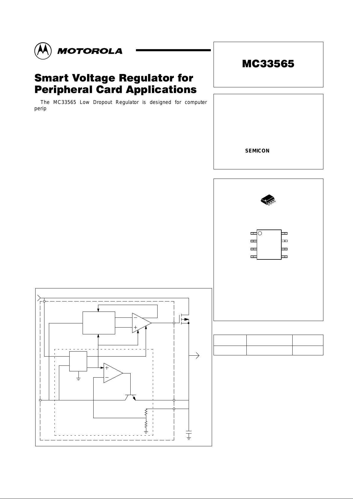
The MC33565 Low Dropout Regulator is designed for computer
peripheral card applications complying with the
instantly available
requirements
as specified by ACPI objectives. The MC33565 permits
glitch–free transitions from “sleep” to “active” system modes and has internal
logic circuitry to detect whether the system is being powered from the
motherboard main 5V power supply or the 3.3V aux supply.
The MC33565 provides a regulated output voltage of 3.3V via either an
internal low drop out 5.0V–to–3.3V voltage regulator or an external P–channel
MOSFET , depending on the operating status of the system in which the card is
installed. During normal operating mode (5V main supply available) the 3.3V
output is provided from the internal low dropout regulator at an output current
of 200mA. When the motherboard enters sleep mode, the MC33565 operates
from the 3.3V aux supply and routes the aux current to the output via the
external P–channel MOSFET bypass transistor controlled by the
drive out
pin.
As a result, the output voltage provided to the peripheral card remains
constant at 3.3V even during transitions to and from sleep mode.
MC33565 Features:
• Output Regulated to 2% Over Temperature
• Output current up to 200mA
• Excellent Line and Load Regulation
• Low Dropout V oltage
• Prevents reverse current flow during sleep mode
• Glitch–free transfer from sleep mode to active mode
• Compatible with
Instantly Available
PC systems
• Evaluation Kit Available: (P.N. MC33565EVK)
Simplified Block Diagram
V
ref
Compensation
&
Hysteresis
+5 Vin
Ref &
Detect
5V detect
Comp
Driver
Drive out
+3.3 Vout
Sense in
+3.3 Vin
Hyst sw
External
P–channel
MOSFET
+3.3 Vout
External
4.7
µ
F
cap
LDO
Motorola, Inc. 1999 Rev 0, 6/99
Page 2
MC33565
2
MOTOROLA ANALOG IC DEVICE DATA
MAXIMUM RATINGS
(TC = 25°C, unless otherwise noted)
Parameter Symbol Max Value Unit
Input Voltage, V
CC
V
max
7.0 Vdc
V
min
–0.5 Vdc
Operating Ambient Temperature T
a
–5 to +70 °C
Operating Junction Temperature T
J
– 5 to +150 °C
Lead Temperature (Soldering, 10 seconds) T
L
300 °C
Storage Temperature Range T
stg
– 55 to +150 °C
Package Thermal Resistance, Junction to Ambient R
θJA
1
180 °C/W
NOTES: 1. Mounted on recommended minimum PCB pad on FR4, 2–oz. copper circuit board.
AC ELECTRICAL SPECIFICATIONS
(3) (4)
Parameter Symbol Min Typ Max Unit
Drive High Delay (Vin ramping up)
C
Drive
= 1.2 nF, measured from +5 Vin = V
thresHi
to V
Drive
= 2V
t
DH
0.5 3.5 µS
Drive Low Delay (Vin ramping down)
C
Drive
= 1.2 nF, measured from +5 Vin = V
thresLo
to V
Drive
= 2V
t
DL
0.5 3.5 µS
NOTES: (1.) See 5V Detect Thresholds Diagram.
(2.) Recommended source impedance for 5V supply: ≤ 0.25W. This will ensure that Io x R
source
< V
hyst
, thus avoiding
driveout toggling during 5V detect threshold transitions.
(3.) See Figure 2. Application Block Diagram.
(4.) See Timing Diagram.
PIN ASSIGNMENTS AND FUNCTIONS
PIN # PIN NAME PIN DESCRIPTION
1 +5 V
in
This is the input supply for the IC. Typical voltage 5 V.
(1) (2)
2,5 N/C Reserved
3 +3.3 V
in
Auxiliary input. Typical voltage 3.3 V.
4 Gnd Logic and Power Gnd.
6 Sense in Load–sense voltage input to internal regulator.
7 +3.3 V
out
3.3V output provided to the application circuit (output current is sourced to this pin from the 5V input.)
8 Drive out
This output drives a P–channel MOSFET with up to 2000pF of “effective” gate capacitance.
Recommended device is MGSF1P02EL T MOSFET. Drive out has active internal pull–up and
pull–down circuitry to guarantee fast transitions.
DEVICE MARKING
Device Type Sub–type Marking (1st Line)
MC33565D 3.3 V MC565
Page 3
MC33565
3
MOTOROLA ANALOG IC DEVICE DATA
DC ELECTRICAL CHARACTERISTICS
(1)
Characteristic Symbol Min Typ Max Unit
+5 Vin Supply Voltage Range +5 V
in
4.3 5.0 5.5 Vdc
Reverse Leakage Current from Output I
reverse
— — 25 µA
V
Aux
quiescent current — — 3.0 mA
+5 Vin quiescent current, operating — — 10 mA
Load Capacitance
(2)
C
load
4.7 22 —
m
F
REGULATOR OUTPUT
Output Voltage
(4.3V ≤ Vin ≤ 5.5V , 0mA ≤ Io ≤ 200mA) TA = 25°C
(TA = –5°C to 150°C)
+3.3 V
out
3.267
3.234
3.30
3.30
3.333
3.366
Vdc
In–to–Out Voltage
(3.9V ≤ Vin ≤ 4.3V , V
aux
= 3.3V)
V
d
3.0 — — Vdc
Voltage Out at Max Voltage In
(Vin = 7V)
V
outmax
3.1 3.3 3.5 Vdc
Line Regulation
(Io = 200 mA)
— — 0.4 %
Load Regulation
(Io = 0 to 200 mA)
— — 0.4 %
5V DETECT
Low Threshold Voltage
(+5 Vin falling)
V
thresLo
3.9 4.05 4.3 Vdc
High Threshold Voltage
(+5 Vin rising)
V
thresHi
— 4.2 4.3 Vdc
Hysteresis V
Hyst
0.12 0.15 0.18 Vdc
DRIVE OUTPUT
Output peak source Current
(+5 Vin > V
thresHi
)
I
peak
15 — — mA
Output peak sink Current
(+5 Vin < V
thresLo
)
I
peak
15 — — mA
Low Output Voltage
(IoL = 200 µA, Vin < V
thresLo
)
V
oL
— 100 200 mVdc
High Output Voltage
(IoH = 200 µA)
V
oH
3.4 V5–0.8 — Vdc
NOTE: 1. (–5°C<Ta<70°C, 4.3V<5V<5.5V , C
load
= 4.7µF unless otherwise noted)
NOTE: 2. 4.7µF minimum over temperature; 22µF recommended; 500mW ESR maximum.
Page 4

MC33565
4
MOTOROLA ANALOG IC DEVICE DATA
V
ref
Compensation
&
Hysteresis
+5 Vin
Ref &
Detect
5V detect
Comp
Driver
Drive out
+3.3 Vout
Sense in
+3.3 Vin
Hyst sw
External
P–channel
MOSFET
+3.3 Vout
External
4.7
µ
F
cap
LDO
Figure 1. Functional Block Diagram
FUNCTIONAL DESCRIPTION
Input Blocking – The internal NPN pass transistor of the
LDO regulator ensures that no significant reverse current will
flow from +3.3 V
out
back to the +5 Vin input when the 5V input
is not powered and the 3.3 Vin supply is present.
5 Volt Detect – Internal circuitry detects the presence of
the 5V input supply. When the 5V supply drops below a given
threshold, the +3.3 Vin bypass transistor (an external
P–channel MOSFET) is enabled. The 5V detect logic is
active throughout the entire range of ramp–up from 0 to 5.5V .
Additionally, the Drive out signal is never turned ON or OFF
inappropriately during ramp–up of the +5 Vin supply. Also,
+3.3 V
out
never drops below 3.0V while +5 Vin is above the
5V detect minimum threshold.
Glitch–free Transfer – The design of the 5V detect
circuitry and Drive out control circuitry guarantees that the
+3.3 V
out
will not exceed the output voltage specification
listed in the table of DC Operating Specifications even with
+5 Vin ramping up and down at the extremes of the slew rates
in the table of AC Operating Specifications (provided the
device is used with an MGSF1P02ELT PMOS FET on Drive
out along with a minimum 4.7µF capacitor on the +3.3 V
out
).
Offset Voltage Performance – To ensure performance
when external offsets are present on the +5 Vin and +3.3 V
in
power inputs, the device has been designed to be capable of
operating with either one or both of these inputs rising from or
falling to zero volts, or with offsets of 0.05V to 0.9V as the
inputs ramp up and down.
Motherboard/
Mainboard
PCI Slot
Figure 2. Application Block Diagram
+5 Vin
N/C
+3.3 Vin
Gnd
Drive out
+3.3 Vout
Sense in
N/C
1
2
3
4
8
7
6
5
MC33565
PCI NIC/Card
Circuitry
5V
3.3V aux
4.7 µF
Page 5

MC33565
5
MOTOROLA ANALOG IC DEVICE DATA
Figure 3. 5V Detect Thresholds Diagram
VIN
3.8V
V
TH(HI)
Figure 4. Timing Diagram
4.4V
2.0V 2.0V
V
TH(LO)
V
HYST
DR
VIN
3.8V
4.4V
2.0V 2.0V
DR
t
DH
t
DL
NOTE:
(1) VIN rise and fall times (10% to 90%) to be
≥
100µs.
NOTE:
(1) VIN rise and fall times (10% to 90%) to be
≤
100ns.
Figure 5. Predicted Gain and Phase
at Zero Load Current
Figure 6. Predicted Gain and Phase
at Full Load Current
or Gain (dB)
0
Frequency (Hz)
100
200
Phase Margin
°
10
1
10
3
10
5
V
out
capacitor 5µF
20m
W
ESR
NOTE: V
out
capacitor
≥
4.7µF over operating temperature range.
Maximum ESR permissable = 500m
W
over operating temperature range.
Phase Margin
°
Gain dB
or Gain (dB)
0
Frequency (Hz)
100
200
Phase Margin
°
10
1
10
3
10
5
V
out
capacitor 5µF
20m
W
ESR
Phase Margin
°
Gain dB
Page 6

MC33565
6
MOTOROLA ANALOG IC DEVICE DATA
D SUFFIX
PLASTIC PACKAGE
CASE 751–06
(SO–8)
ISSUE T
OUTLINE DIMENSIONS
SEATING
PLANE
1
4
58
A0.25MCB
SS
0.25MB
M
h
q
C
X 45
_
L
DIM MIN MAX
MILLIMETERS
A 1.35 1.75
A1 0.10 0.25
B 0.35 0.49
C 0.19 0.25
D 4.80 5.00
E
1.27 BSCe
3.80 4.00
H 5.80 6.20
h
0 7
L 0.40 1.25
q
0.25 0.50
__
NOTES:
1. DIMENSIONING AND TOLERANCING PER ASME
Y14.5M, 1994.
2. DIMENSIONS ARE IN MILLIMETER.
3. DIMENSION D AND E DO NOT INCLUDE MOLD
PROTRUSION.
4. MAXIMUM MOLD PROTRUSION 0.15 PER SIDE.
5. DIMENSION B DOES NOT INCLUDE DAMBAR
PROTRUSION. ALLOWABLE DAMBAR
PROTRUSION SHALL BE 0.127 TOTAL IN EXCESS
OF THE B DIMENSION AT MAXIMUM MATERIAL
CONDITION.
D
E
H
A
B
e
B
A1
C
A
0.10
Page 7

MC33565
7
MOTOROLA ANALOG IC DEVICE DATA
NOTES
Page 8

MC33565
8
MOTOROLA ANALOG IC DEVICE DATA
Motorola reserves the right to make changes without further notice to any products herein. Motorola makes no warranty , representation or guarantee regarding
the suitability of its products for any particular purpose, nor does Motorola assume any liability arising out of the application or use of any product or circuit, and
specifically disclaims any and all liability, including without limitation consequential or incidental damages. “T ypical” parameters which may be provided in Motorola
data sheets and/or specifications can and do vary in different applications and actual performance may vary over time. All operating parameters, including “Typicals”
must be validated for each customer application by customer’s technical experts. Motorola does not convey any license under its patent rights nor the rights of
others. Motorola products are not designed, intended, or authorized for use as components in systems intended for surgical implant into the body, or other
applications intended to support or sustain life, or for any other application in which the failure of the Motorola product could create a situation where personal injury
or death may occur. Should Buyer purchase or use Motorola products for any such unintended or unauthorized application, Buyer shall indemnify and hold Motorola
and its officers, employees, subsidiaries, affiliates, and distributors harmless against all claims, costs, damages, and expenses, and reasonable attorney fees
arising out of, directly or indirectly, any claim of personal injury or death associated with such unintended or unauthorized use, even if such claim alleges that
Motorola was negligent regarding the design or manufacture of the part. Motorola and are registered trademarks of Motorola, Inc. Motorola, Inc. is an Equal
Opportunity/Affirmative Action Employer.
Mfax is a trademark of Motorola, Inc.
How to reach us:
USA/EUROPE /Locations Not Listed: Motorola Literature Distribution; JAPAN: Motorola Japan Ltd.; SPD, Strategic Planning Office, 141,
P.O. Box 5405, Denver, Colorado 80217. 1–303–675–2140 or 1–800–441–2447 4–32–1 Nishi–Gotanda, Shinagawa–ku, Tokyo, Japan. 81–3–5487–8488
Customer Focus Center: 1–800–521–6274
Mfax: RMFAX0@email.sps.mot.com – TOUCHTONE 1–602–244–6609 ASIA/PACIFIC: Motorola Semiconductors H.K. Ltd.; Silicon Harbour Centre,
Motorola Fax Back System – US & Canada ONLY 1–800–774–1848 2, Dai King Street, Tai Po Industrial Estate, Tai Po, N.T., Hong Kong.
– http://sps.motorola.com/mfax/ 852–26629298
HOME PAGE: http://motorola.com/sps/
MC33565/D
◊
 Loading...