

Page 1
Order this document by MC33470/D
The MC33470 is a digitally programmable switching voltage regulator,
specifically designed for Microprocessor supply, Voltage Regulator Module
and general purpose applications, to provide a high power regulated output
voltage using a minimum of external parts. A 5–bit digital–to–analog converter
defines the dc output voltage.
This product has three additional features. The first is a pair of high speed
comparators which monitor the output voltage and expedite the circuit
response to load current changes. The second feature is a soft start circuit
which establishes a controlled response when input power is applied and
when recovering from external circuit fault conditions. The third feature is two
output drivers which provide synchronous rectification for optimum
efficiency.
This product is ideally suited for computer, consumer, and industrial
equipment where accuracy, efficiency and optimum regulation performance
is desirable.
MC33470 Features:
• 5–Bit Digital–to–Analog Converter Allows Digital Control of
Output Voltage
• High Speed Response to Transient Load Conditions
• Output Enable Pin Provides On/Off Control
• Programmable Soft Start Control
• High Current Output Drives for Synchronous Rectification
• Internally Trimmed Reference with Low Temperature Coefficient
• Programmable Overcurrent Protection
• Overvoltage Fault Indication
• Functionally Similar to the L TC1553
SYNCHRONOUS
RECTIFICATION DC/DC
CONVERTER
PROGRAMMABLE
INTEGRATED CONTROLLER
SEMICONDUCTOR
TECHNICAL DATA
20
1
DW SUFFIX
PLASTIC PACKAGE
CASE 751D
(SO–20L)
PIN CONNECTIONS
G2
P
V
CC
P
Gnd
A
Gnd
V
CC
Sense
I
max
I
fb
SS
Compensation
1
2
3
4
5
6
7
8
9
10
20
19
18
17
16
15
14
13
12
11
G1
OUTEN
VID0
VID1
VID2
VID3
VID4
P
wrgd
Fault
OT
This document contains information on a new product. Specifications and information herein
are subject to change without notice.
MOTOROLA ANALOG IC DEVICE DATA
(Top View)
ORDERING INFORMATION
Operating
Device
MC33470DW SO–20LTA = 0° to +75°C
Motorola, Inc. 1997 Rev 0
Temperature Range
Package
1
Page 2
Voltage
Á
Á
Á
Á
Identification
Code
Input
Sense
Power
Good
MC33470
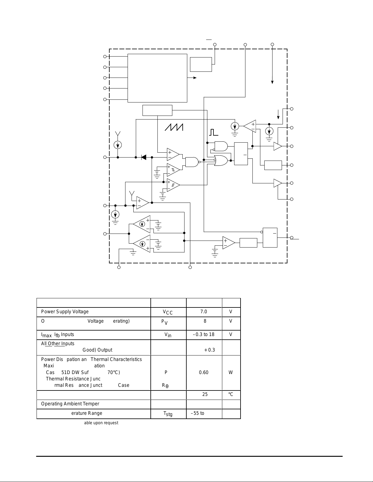
Simplified Block Diagram
18
VID0
17
VID1
16
VID2
15
VID3
14
VID4
V
CC
10
9
SS
6
20 µA
13
Digitally Programmed
Reference
Oscillator
µ
A
0.96 V
ref
V
ref
800
µ
OTA Error Amp
1.5 V
+
+
+
+
PWM
Comparator
1.04 V
ref
1.04 V
ref
0.93 V
ref
2.5 V
Over
Temp
V
ref
1.14 V
OT
ref
11
90
Outen
Over Current
µ
A
S
R
PWM
Latch
5
V
19
CC
V
CC
7
Detect
En
Q
Q
190 µA
Delay
I
2
P
20
G1
8
I
1
G2
3
P
R
Delay Fault
S
14
Q
max
V
CC
fb
Gnd
Compensation
MAXIMUM RATINGS (T
A
410
Gnd
= 25°C, unless otherwise noted.)
C
Rating Symbol Value Unit
Power Supply Voltage
Output Driver Supply Voltage (Operating)
ББББББББББББ
I
, Ifb Inputs
max
All Other Inputs and Digital
V
CC
P
V
ÁÁ
CC
V
in
V
in
ÁÁÁ
–0.3 to 18
–0.3 to
(OT, Fault, Power Good) Outputs VCC + 0.3
Power Dissipation and Thermal Characteristics
Maximum Power Dissipation
Case 751D DW Suffix (TA = 70°C)
Thermal Resistance Junction–to–Ambient
Thermal Resistance Junction–to–Case
Operating Junction Temperature
Operating Ambient Temperature (Notes 1 and 2)
Storage Temperature Range
NOTE: ESD data available upon request
R
R
T
P
θJA
θJC
T
T
stg
D
J
A
0 to +70
–55 to +125
7.0
18
0.60
91
60
125
V
V
Á
V
V
W
°C/W
°C/W
°C
°C
°C
2
MOTOROLA ANALOG IC DEVICE DATA
Page 3
MC33470
ÁÁÁ
ÁÁÁ
ÁÁÁ
ÁÁÁ
ÁÁÁ
ÁÁÁ
ÁÁÁ
ÁÁÁ
ÁÁÁ
ÁÁÁ
ÁÁÁ
ÁÁÁ
ÁÁÁ
ÁÁÁ
ÁÁÁ
ÁÁÁ
ÁÁÁ
ÁÁÁ
ÁÁÁ
ÁÁÁ
ÁÁÁ
ÁÁÁ
ÁÁÁ
ÁÁÁ
ÁÁÁ
ÁÁÁ
ÁÁÁ
ÁÁÁ
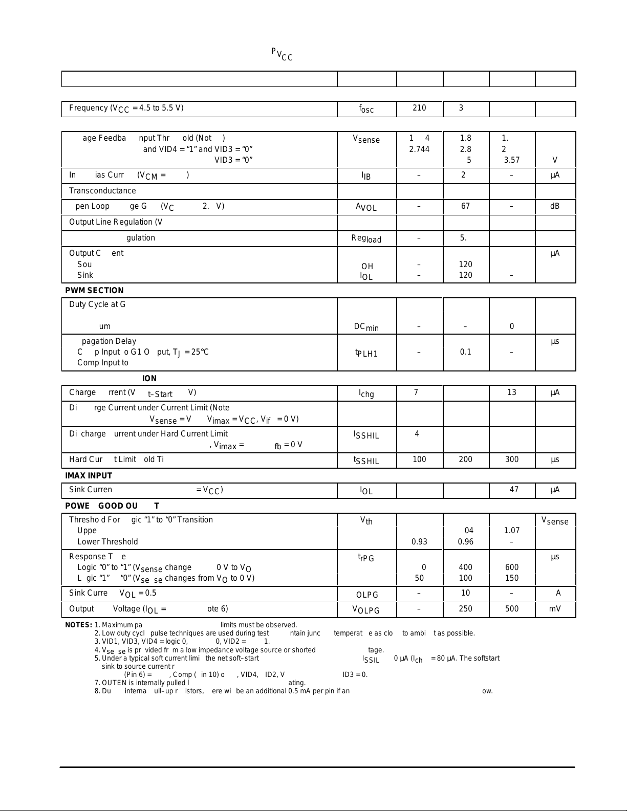
ELECTRICAL CHARACTERISTICS (V
min/max values TA is the operating ambient temperature range that applies, unless otherwise noted.)
Characteristic
= 5.0 V, P
CC
, = 12 V for typical values TA = Low to High [Notes 1, 2, 3], for
P
VCC
V
CC
Symbol Min Typ Max Unit
OSCILLAT OR
Frequency (VCC = 4.5 to 5.5 V)
f
osc
210
FEEDBACK AMPLIFIER
Voltage Feedback Input Threshold (Note 4)
VID0, VID1, VID2 and VID4 = “1” and VID3 = “0”
VID4 = “1” and VID0, VID1, VID2 and VID3 = “0”
Input Bias Current (VCM = 2.8 V)
Transconductance (VCM = 2.8 V, V
Open Loop Voltage Gain (V
COMP
COMP
= 2.0 V)
= 2.0 V)
Output Line Regulation (VCC = 4.5 to 5.5 V)
Output Load Regulation
V
sense
A
Reg
Reg
I
IB
G
M
VOL
load
line
1.764
2.744
3.43
–
400
–
–
–
Output Current
Source
Sink
I
I
OH
OL
–
–
PWM SECTION
Duty Cycle at G1 Output
Maximum
Minimum
DC
DC
max
min
77
–
Propagation Delay
Comp Input to G1 Output, TJ = 25°C
Comp Input to G2 Output, TJ = 25°C
t
PLH1
t
PLH2
–
–
SOFT–START SECTION
Charge Current (V
Soft–Start
Discharge Current under Current Limit (Note 5)
(V
Soft–Start
= 2.0 V, V
Discharge Current under Hard Current Limit
(V
Soft–Start
= 2.0 V, V
Hard Current Limit Hold Time
sense
sense
= 0 V)
= V
< V
out
out
, V
/2, V
imax
imax
= VCC, V
= VCC, V
ifb
ifb
= 0 V)
= 0 V)
I
chg
I
SSIL
I
SSHIL
t
SSHIL
7.0
30
40
100
IMAX INPUT
Sink Current (Vin
max
= VCC, V
= VCC)
ifb
I
OL
133
POWER GOOD OUTPUT
Threshold For Logic “1” to “0” Transition
Upper Threshold
Lower Threshold
Response Time
Logic “0” to “1” (V
Logic “1” to “0” (V
changes from 0 V to VO)
sense
changes from VO to 0 V)
sense
Sink Current (VOL = 0.5 V)
Output Low Voltage (IOL = 100 µA) (Note 6)
NOTES: 1. Maximum package power dissipation limits must be observed.
2.Low duty cycle pulse techniques are used during test to maintain junction temperature as close to ambient as possible.
3.VID1, VID3, VID4 = logic 0, and VID0, VID2 = logic 1.
4.V
5.Under a typical soft current limit, the net soft–start discharge current will be 90 µA (I
6 Sense (Pin 6) = 5.0 V, Comp (Pin 10) open, VID4, VID2, VID1, VID0 = 1.0, VID3 = 0.
7.OUTEN is internally pulled low if VID0, 1, 2, 3, and 4 are floating.
8.Due to internal pull–up resistors, there will be an additional 0.5 mA per pin if any of the VID0, 1, 2, 3, or 4 pins are pulled low.
is provided from a low impedance voltage source or shorted to the output voltage.
sense
sink to source current ratio is designed to be 9:1.
V
t
rPG
I
OLPG
V
OLPG
th
SSIL
) – 10 µA (I
–
0.93
200
50
–
–
chg
300
1.8
2.8
3.5
20
800
67
7.0
5.0
120
120
88
–
0.1
0.1
10
90
64
200
190
1.04
0.96
400
100
10
250
) = 80 µA. The softstart
390
1.836
2.856
3.57
–
1200
–
–
–
–
–
95
0
–
–
13
150
–
300
247
1.07
–
600
150
–
500
kHz
µA
µmho
dB
mV
mV
µA
µA
µA
mA
µA
V
sense
mA
mV
V
V
V
%
µs
µs
µs
MOTOROLA ANALOG IC DEVICE DATA
3
Page 4
MC33470
ÁÁÁ
ÁÁÁ
ÁÁÁ
ÁÁÁ
ÁÁÁ
ÁÁÁ
ÁÁÁ
ÁÁÁ
ÁÁÁ
ÁÁÁ
ÁÁÁ
ÁÁÁ
ÁÁÁ
ÁÁÁ
ÁÁÁ
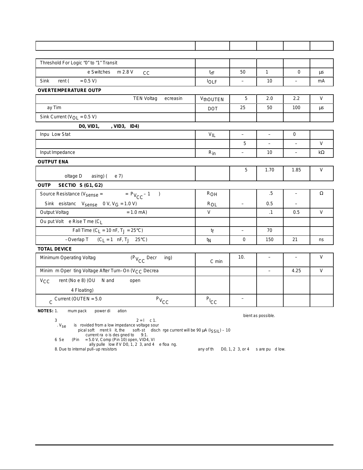
ELECTRICAL CHARACTERISTICS
min/max values TA is the operating ambient temperature range that applies, unless otherwise noted.)
(continued) (VCC = 5.0 V, P
, = 12 V for typical values TA = Low to High [Notes 1, 2, 3], for
P
VCC
V
CC
Characteristic UnitMaxTypMinSymbol
FAULT OUTPUT
Threshold For Logic “0” to “1” Transition
V
Response Time Switches from 2.8 V to V
sense
Sink Current (VOL = 0.5 V)
CC
V
t
I
OLF
thF
rF
1.12
50
–
OVERTEMPERATURE OUTPUT
Threshold For Logic “1” to “0” Transition (OUTEN V oltage Decreasing)
Delay Time
Sink Current (VOL = 0.5 V)
V
thOUTEN
t
DOT
I
OLF
1.85
25
–
LOGIC INPUTS (VID0, VID1, VID2, VID3, VID4)
Input Low State
Input High State
Input Impedance
V
IL
V
IH
R
in
–
3.5
–
OUTPUT ENABLE CONTROL (OUTEN)
Over–Temperature Driver Disable and Reset
V
OTDD
1.55
(OUTEN Voltage Decreasing) (Note 7)
OUTPUT SECTIONS (G1, G2)
= 1.0 mA)
sink
P
VCC
V
– 1.0 V)
CC
Source Resistance (V
Sink Resistance (V
= 2.0 V, VG = P
sense
= 0 V, VG = 1.0 V)
sense
Output Voltage with OUTEN Reset (I
Output Voltage Rise T ime (CL = 10 nF, TJ = 25°C)
Output Voltage Fall T ime (CL = 10 nF, TJ = 25°C)
G1, G2 Non–Overlap Time (CL = 10 nF, TJ = 25°C)
R
R
V
t
NOL
OH
OL
OL
t
r
t
f
– 0.5 – Ω
–
–
–
–
30
TOTAL DEVICE
Minimum Operating Voltage After Turn–On (P
P
VCC
V
CC
Decreasing)
Minimum Operating Voltage After Turn–On (VCC Decreasing)
VCC Current (Note 8) (OUTEN and P
P
VCC
V
CC
open,
P
V
CC min
VCC
I
min
CC
10.8 – – V
3.0
– 3.7 8.0 mA
VID0, 1, 2, 3, 4 Floating)
P
P
Current (OUTEN = 5.0 V, VID0, 1, 2, 3, 4 Open, P
VCC
V
CC
NOTES: 1. Maximum package power dissipation limits must be observed.
2.Low duty cycle pulse techniques are used during test to maintain junction temperature as close to ambient as possible.
3.VID1, VID3, VID4 = logic 0, and VID0, VID2 = logic 1.
4.V
5.Under a typical soft current limit, the net soft–start discharge current will be 90 µA (I
6 Sense (Pin 6) = 5.0 V, Comp (Pin 10) open, VID4, VID2, VID1, VID0 = 1.0, VID3 = 0.
7.OUTEN is internally pulled low if VID0, 1, 2, 3, and 4 are floating.
8.Due to internal pull–up resistors, there will be an additional 0.5 mA per pin if any of the VID0, 1, 2, 3, or 4 pins are pulled low.
is provided from a low impedance voltage source or shorted to the output voltage.
sense
sink to source current ratio is designed to be 9:1.
P
VCC
V
CC
= 12 V)
P
I
CC
SSIL
) – 10 µA (I
– 15 – mA
chg
1.14
100
10
2.0
50
10
–
–
10
1.70
0.5
0.1
70
70
150
–
) = 80 µA. The softstart
1.2
150
–
2.2
100
–
0.8
–
–
1.85
–
0.5
140
140
210
4.25
V
µs
mA
µs
mA
kΩ
ns
ns
ns
ref
V
V
V
V
V
V
4
MOTOROLA ANALOG IC DEVICE DATA
Page 5
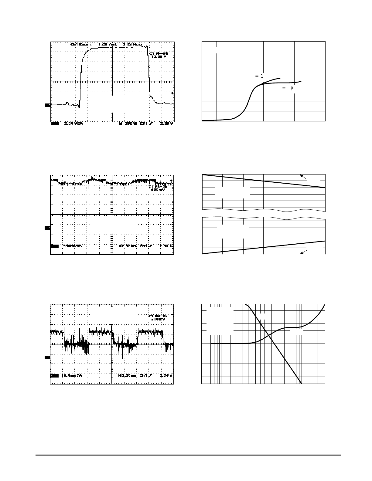
Figure 1. Output Drive Waveform Figure 2. 5.0 V Supply Current
2.0 V/DIV500 mV/DIV50 mV/DIV
VO = 2.8 V
IO = 3.3 A
Figure 13 Circuit
200 nS/DIV
Figure 3. Error Amplifier Transient Response
MC33470
8.0
7.0
6.0
5.0
4.0
3.0
, SUPPLY CURRENT (mA)
2.0
CC
I
1.0
0
0
–0.5
–1.0
TA = 25°C
P
+
12 V
V
CC
P
+
Open
V
CC
0 1.0 2.0 3.0 4.0 5.0 6.0
INPUT VOLTAGE (V)
7.0
Figure 4. Drive Output Source/Sink Saturation
V oltage versus Load Current
P
Source Saturation
(Load to Ground)
V
8.0
CC
VO = 2.8 V
0
IO transient = 0.3 to 16 A
Figure 13 Circuit
2.5 mS/DIV
1.0
0.5
0
Figure 5. Feedback Circuit Load
Transient Response
20
VO = 2.8 V
IO transient = 0.3 to 16 A
Figure 13 Circuit
2.5 mS/DIV
15
10
5.0
LOOP GAIN (dB)
0
–5.0
–10
300
Sink Saturation
(Load to P
0 0.2 0.4 0.6 0.8 1.0 1.2
)
V
CC
Ground
Figure 6. Feedback Loop Gain and Phase
versus Frequency
V
= 12 V
CCP
VCC = 5.0 V
VO = 2.8 V
IO = 3.3 A
°
C
TA = 25
1.0 k 10 k 100 k 300 k3.0 k 30 k
Gain
Phase
f, FREQUENCY (Hz)
0
30
60
90
120
, EXCESS PHASE (DEGREES)
∅
150
180
MOTOROLA ANALOG IC DEVICE DATA
5
Page 6

MC33470
Figure 7. Drive Output Source/Sink Saturation
V oltage versus Load Current
1000
Gain
V
= 12 V
CCP
100
VCC = 5.0 V
µ
GAIN ( mho)
, CURRENT CHANGE (%)
max
I
VO = 2.8 V
R2 = 18.2 k
C16 = 0
°
C
TA = 25
10
Figure 13
1.0
1.0 10 100 1000
FREQUENCY (kHz)
4.0
2.0
–2.0
–4.0
–6.0
Figure 9. I
0
–50 –25 0 25 50 75
Current versus Temperature
max
TA, AMBIENT TEMPERATURE (
Phase
°
C)
IO = 3.3 A
VO = 2.8 V
Figure 8. Feedback Threshold V oltage
versus T emperature
0
30
60
90
120
150
180
0.8
0.6
0.4
0.2
, EXCESS PHASE (DEGREES)
∅
0
THRESHOLD VOLTAGE CHANGE (%)
–0.2
–50 –25 0 25 50 75
–75
TA, AMBIENT TEMPERATURE (
Figure 10. V
Current Source
sense
IO = 3.3 A
VO = 2.8 V
°
C)
100 125
versus T emperature
5.0
4.0
IO = 3.3 A
VO = 2.8 V
2.0
0
, CURRENT CHANGE (%)
–2.0
sense
I
–4.0
100 125–75
–5.0
–50 –25 0 25 50 75
TA, AMBIENT TEMPERATURE (
°
C)
100 125–75
Figure 11. VCC Undervoltage Lockout Trip Point
versus T emperature
1.0
0.5
0
–0.5
–1.0
–1.5
–2.0
–2.5
–3.0
UVLO THRESHOLD CHANGE (%)
–3.5
–4.0
–50 –25 0 25 50 75
TA, AMBIENT TEMPERATURE (
VCC Increasing
IO = 3.3 A
VO = 2.8 V
°
C)
6
Figure 12. Oscillator Frequency
versus T emperature
2.5
2.0
1.5
IO = 3.3 A
VO = 2.8 V
1.0
0.5
0
–0.5
–1.0
–1.5
UVLO THRESHOLD CHANGE (%)
–2.0
100 125–75
–2.5
–50 –25 0 25 50 75
TA, AMBIENT TEMPERATURE (
°
C)
100 125–75
MOTOROLA ANALOG IC DEVICE DATA
Page 7

= 5.0 V
in
V
Input Voltage
µ
L2
1.5 H
J1–A1, A2, A3, B1, B2
R10
MC33470
Figure 13. MC33470 Application Circuit
VO0.3 to 14 A
J1–A10, A12, A14,
A16, A18, A20,
B11, B13, B15,
B17, B19
F
µ
C2
150
16 V
F
µ
C1
150
16 V
++
C5
470 pF
12 V
J1–A4, B4
max
+
R9
7
4.0/3.8
R1
µ
2.7 k
C3
4.7 F
I
CC
10
5
CC
V
V
Q1
µ
1.0 F
µ
190 A
Detect
MMSF3300R2
V DRIVE
µ
90 A
≤
10
C6
+
Over Current
5, 6, 7, 8
R8
2
En
H
µ
L1
1.5
Q2
MMSF3300R2
5, 6, 7, 8
2, 3
4
56
R4
4.7
fb
I
G1
20
Delay
Q3
5, 6, 7, 8
MMSF3300R2
G2
8
1
R7
4.7
Gnd
P
µ
C13
1.0 F
F
µ
C11
4.0 V
820
F
µ
C10
4.0 V
820
D2
MBRD1035CT
Q4
2, 3
4
3
MMSF3300R2
VSSJ1–A11, A13, A15
Fault Indicate
R6
12
Fault
Q
S
R
Delay
A17, A19, B10, B12
B14, B16, B18, B20
100 k
U1
R5
1.2 k
J1 – AMP 532956–7
L1, L2 – Coilraft U6904
J1–B6
OUTEN
D1
UP#
J1–B5
11 19OUTEN
OT
ref
V
Over
T emp
Digitally Programmed
VID018
VID1
VID2
171615
J1–A7
J1–B7
J1–A8
Voltage
Identification
Lockout
Undervoltage
Reference
VID3
VID4
14
J1–B8
J1–A9
Input
Code
Oscillator
2.5 V
CC
V
S
PWM
Comparator
1.5 V
µ
10 A
SS
Q
R
PWM
Latch
ref
/2
ref
V
9
C18
µ
0.01 F
+
ref
0.96 V
64 mA
+
ref
V
ref
1.04 V
µ
800
Sense
OTA Error Amp
6
1.14 V
ref
ref
1.04 V
0.96 V
+
+
µ
20 A
13
Good
Power
R3
100 k
µ
J1–B9
To P
Compensation10
Gnd
A4
C16
2200 pF
C17
R2
8.2 k
100 pF
C3 – TDK C3216Y5V1C476Z
C1, C2 – OSCON 16SA150M
C6, C13 – TDK C3216Y5V1C106Z
C10, C11– OSCON 4SP820M
MOTOROLA ANALOG IC DEVICE DATA
7
Page 8

12 V
5.0 V
Internal
V
ref
MC33470
Figure 14. Timing Diagram
UVL Threshold
UVL Threshold
2.5 V
1.5 V
Compensation
G1
G2
OPERA TING DESCRIPTION
The MC33470 is a monolithic, fixed frequency power
switching regulator specifically designed for dc–to–dc
converter applications which provide a precise supply
voltage for state of the art processors. The MC33470
operates as fixed frequency, voltage mode regulator
containing all the active functions required to directly
implement digitally programmable step–down synchronous
rectification with a minimum number of external components.
Oscillator
The oscillator frequency is internally programmed to
300 kHz. The charge to discharge ratio is controlled to yield
a 95% maximum duty cycle at the switch outputs. During the
fall time of the internal sawtooth waveform, the oscillator
generates an internal blanking pulse that disables the G1
output switching MOSFET. The internal sawtooth waveform
has a nominal peak voltage of 2.5 V and a valley voltage of
1.5 V.
Pulse Width Modulator
The pulse width modulator consists of a comparator with
the oscillator ramp voltage applied to the noninverting input,
while the error amplifier output is applied to the inverting
input. Output switch conduction is initiated when the ramp
waveform is discharged to the valley voltage. As the ramp
voltage increases to a voltage that exceeds the error amplifer
output, the latch resets, terminating output G1 MOSFET
conduction, and turning on output G2 MOSFET, for the
duration of the oscillator ramp. This PWM/latch combination
Timing Capacitor
prevents multiple output pulses during a given oscillator
cycle.
The sense voltage input at Pin 6 is applied to the
noninverting inputs of a pair of high speed comparators. The
high speed comparators’ inverting inputs are tied 0.96 x V
and 1.04 x V
, respectively, to provide an optimum response
ref
ref
to load changes. When load transients which cause the
output voltage to fall outside a "4% regulation window occur,
the high speed comparators override the PWM comparator to
force a zero or maximum duty cycle operating condition until
the output voltage is once again within the linear window.
When voltages are initially provided to the supply pins,
VCC and
, undervoltage lockout circuits monitor each
P
V
CC
of the supply voltage levels. Both G1 and G2 output pins are
held low until the VCC pin voltage exceeds 4.0 V and the
pin voltage exceeds 9.0 V.
P
V
CC
Error Amplifier and Voltage Reference
The error amplifier is a transconductance type amplifier,
having a nominal transconductance of 800 µmho. The
transconductance has a negative temperature coefficient.
Typical transconductance is 868 µmho at 0°C and 620 µmho
at 125°C junction temperature. The amplifier has a cascode
output stage which provides a typical 3.0 Mega–Ohms of
impedance. The typical error amplifier dc voltage gain is 67 dB.
External loop compensation is required for converter
stability . Compensation components may be connected from
8
MOTOROLA ANALOG IC DEVICE DATA
Page 9

MC33470
the compensation pin to ground. The error amplifier input is
tied to the sense pin which also has an internal 20 µA current
source to ground. The current source is intended to provide a
24 mV offset when an external 1.2 k resistor is placed
between the output voltage and the sense pin. The 24 mV
offset voltage is intended to allow a greater dynamic load
regulation range within a given specified tolerance for the
output voltage. The offset may be increased by increasing
the resistor value. The offset can be eliminated by connecting
the sense pin directly to the regulated output voltage.
The voltage reference consists of an internal, low
temperature coefficient, reference circuit with an added offset
voltage. The offset voltage level is the output of the
digital–to–analog converter. Control bits VID0 through VID4
control the amount of offset voltage which sets the value of
the voltage reference, as shown in T able 1. The VID0–4 input
bits each have internal 10 k pullup resistances. Therefore,
the reference voltage, and the output voltage, may be
programmed by connecting the VID pins to ground for logic
“0” or by an open for a logic “1”. Typically, a logic “1” will be
recognized by a voltage > 0.67 x VCC. A logic “0” is a voltage
< VCC/3.
MOSFET Switch Outputs
The output MOSFETs are designed to switch a maximum
of 18 V, with a peak drain current of 2.0 A. Both G1 and G2
output drives are designed to switch N–channel MOSFETs.
Output drive controls to G1 and G2 are phased to prevent
cross conduction of the internal IC output stages. Output
dead time is typically 100 nanoseconds between G1 and G2
in order to minimize cross conduction of the external
switching MOSFETs.
Current Limit and Soft–Start Controls
The soft–start circuit is used both for initial power
application and during current limit operation. A single
external capacitor and an internal 10 µA current source
control the rate of voltage increase at the error amplifier
output, establishing the circuit turn on time. The G1 output
will increase from zero duty cycle as the voltage across the
soft–start capacitor increases beyond about 0.5 V. When the
soft–start capacitor voltage has reached about 1.5 V, normal
duty cycle operation of G1 will be allowed.
An overcurrent condition is detected by the current limit
amplifier. The current limit amplifier is activated whenever the
G1 output is high. The current limit amplifier compares the
voltage drop across the external MOSFET driven by G1, as
measured at the IFB pin, with the voltage at the I
Because the I
pin draws 190 µA of input current, the
max
overcurrent threshold is programmed by an external resistor.
max
pin.
Referring to Figure 13, the current limit resistor value can be
determined from the following equation:
R1
[(I
+
L(max)
(I
)(R
max
DS(on)
)
)]
where:
IO)
I
I
L(max)
= Maximum load current
I
O
= Inductor peak to peak ripple current
I
ripple
+
ripple
2
OUTEN Input and OT Output Pins
On and off control of the MC33470 may be implemented
with the OUTEN pin. A logic “1” applied the OUTEN pin,
where a logic “1” is above 2.0 V , will allow normal operation of
the MC33470. The OUTEN pin also has multiple thresholds
to provide over temperature protection. An negative
temperature coefficient thermistor can be connected to the
OUTEN pin, as shown in Figure 15. Together with RS, a
voltage divider is formed. The divider voltage will decrease
as the thermistor temperature increases. Therefore, the
thermistor should be mounted to the hottest part on the circuit
board. When the OUTEN voltage drops below 2.0 V typically ,
the MC33470 OT pin open collector output will switch from a
logic “1” to a logic “0”, providing a warning to the system. If
the OUTEN voltage drops below 1.7 V, both G1 and G2
output driver pins are latched to a logic “0” state.
Figure 15. OUTEN/OT Overtemperature Function
V
CC
10 k
OT
V
CC
R
S
OUTEN
NTC
Thermistor
MC33470
APPLICATIONS INFORMATION
Design Example
Given the following requirements, design a switching
dc–to–dc converter:
V
= 5.0 V
CC
V
= 12 V
CCP
VID4–0 bits
Output current
Efficiency >
80% at full load
Output ripple voltage ≈ 1% of output voltage
MOTOROLA ANALOG IC DEVICE DATA
= 1011 1 – Output Voltage = 2.8 V
= 0.3 A to 14 A
1. Choose power MOSFETs.
In order to meet the efficiency requirement, MOSFETs
should be chosen which have a low value of R
DS(on)
However, the threshold voltage rating of the MOSFET must
also be greater than 1.5 V, to prevent turn on of the
synchronous rectifier MOSFETs due to dv/dt coupling
through the Miller capacitance of the MOSFET
drain–to–source junction. Figure 16 shows the gate voltage
transient due to this effect.
9
.
Page 10

MC33470
In this design, choose two parallel MMSF3300 MOSFETs
for both the main switch and the synchronous rectifier to
maximize efficiency.
2. D ≈ VO/Vin = 2.8/5.0 = 0.56
3. Inductor selection
In order to maintain continuous mode operation at 10% of
full load current, the minimum value of the inductor will be:
L
= (Vin – VO)(DTs)/(2IO
min
= (5 – 2.8)(0.56 x 3.3 µs)/(2 x 1.4 A) = 1.45 µH
Coilcraft’s U6904, or an equivalent, provides a surface
mount 1.5 µH choke which is rated for for full load current.
4. Output capacitor selection
V
≈ ∆ IL x ESR, where ESR is the equivalent series
ripple
resistance of the output capacitance. Therefore:
ESR
maximum
The AVX TPS series of tantalum chip capacitors may be
chosen. Or OSCON capacitors may be used if leaded parts
are acceptable. In this case, the output capacitance consists
of two parallel 820 µF , 4.0 V capacitors. Each capacitor has a
maximum specified ESR of 0.012 Ω.
5. Input Filter
As with all buck converters, input current is drawn in
pulses. In this case, the current pulses may be 14 A peak. If
a 1.5 µH choke is used, two parallel OSCON 150 µF, 16 V
capacitors will provide a filter cutoff frequency of 7.5 kHz.
6. Feedback Loop Compensation
The corner frequency of the output filter with L = 1.5 µH
and Co = 1640 µF is 3.2 kHz. In addition, the ESR of each
output capacitor creates a zero at:
fz = 1/(2π C ESR) = 1/(2π x 820 µF x 0.012) = 16.2 kHz
The dc gain of the PWM is: Gain = Vin/Vpp = 5/1 = 5.0.
Where Vpp is the peak–to–peak sawtooth voltage across the
internal timing capacitor. In order to make the feedback loop
as responsive as possible to load changes, choose the
max
= V
/∆ IL = 0.01 x 2.8 V/1.4 A = 0.02 Ω
ripple
min
)
unity gain frequency to be 10% of the switching frequency,
or 30 kHz. Plotting the PWM gain over frequency, at a
frequency of 30 kHz the gain is about –16.5 dB = 0.15.
Therefore, to have a 30 kHz unity gain loop, the error
amplifier gain at 30 kHz should be 1/0.15 = 6.7. Choose a
design phase margin for the loop of 60°. Also, choose the
error amp type to be an integrator for best dc regulation
performance. The phase boost needed by the error amplifier
is then 60° for the desired phase margin. Then, the following
calculations can be made:
k = tan [Boost/2 + 45°] = tan [60/2 + 45] = 3.73
Error Amp zero freq = fc/K = 30 kHz/3.73 = 8.0 kHz
Error Amp pole freq = Kfc = 3.73 x 30 kHz = 112 kHz
R2 = Error Amp Gain/Gm = 6.7/800 µ = 8.375 k – use an
8.2 k standard value
C16 = 1/(2π R2 fz) = 1/(2π x 8.2 k x 8.0 kHz) = 2426 pF –
use 2200 pF
C17 = 1/(2π R2 fp) = 1/(2π x 8.2 k x 112 kHz) = 173 pF –
use 100 pF
The complete design is shown in Figure 13. The PC board
top and bottom views are shown in Figures 17 and 18.
Figure 16. V oltage Coupling Through Miller
Capacitance
10
MOTOROLA ANALOG IC DEVICE DATA
Page 11

Pin Name Description
Á
Á
Á
Á
Á
Á
Á
Á
Á
Á
Á
Á
Á
Á
Á
Á
Á
Á
Á
Á
Á
Á
Á
Á
Á
Á
Á
Á
Á
Á
Á
Á
Á
Á
Á
Á
Á
Á
Á
Á
Á
Á
Á
Á
Á
Á
Á
Á
Á
Á
Á
Á
Á
Á
1 G2 This is a high current dual totem pole output Gate Drive for the Lower, or rectifier, N–channel
2
БББББ
3
4
5
БББББ
6
7
БББББ
8
БББББ
БББББ
9
БББББ
БББББ
10
БББББ
11
БББББ
12
БББББ
13
БББББ
14
БББББ
15
БББББ
16
БББББ
17
18
БББББ
19
БББББ
БББББ
20
БББББ
БББББ
P
V
CC
ÁÁÁ
P
Gnd
A
Gnd
V
CC
Sense
ÁÁÁ
I
max
ÁÁÁ
I
FB
ÁÁÁ
ÁÁÁ
SS
ÁÁÁ
ÁÁÁ
Comp
ÁÁÁ
OT
ÁÁÁ
Fault
ÁÁÁ
P
wrgd
ÁÁÁ
VID4
ÁÁÁ
VID3
ÁÁÁ
VID2
VID1
ÁÁÁ
VID0
ÁÁÁ
OUTEN
ÁÁÁ
ÁÁÁ
G1
ÁÁÁ
ÁÁÁ
MC33470
PIN FUNCTION DESCRIPTION
MOSFET. Its output swings from ground to . During initial power application, both G2
and G1 are held low until both VCC and have reached proper levels.
This is a separate power source connection for driving N–channel MOSFETs from the G1 and
G2 outputs. It may be connected to 12 V .
ББББББББББББББББББББББ
This is a separate power ground return that is connected back to the power source. It is used to
reduce the effects of switching transient noise on the control circuitry .
This pin is the ground for the control circuitry.
This pin is the positive supply of the control IC.
This pin is used for feedback from the output of the power supply. It has a 20 µA current source
ББББББББББББББББББББББ
to ground which can be used to provide offset in the converter output voltage.
This pin sets the current limit threshold. 190 µA must be sourced into the pin. The external
resistor is determined from the following equation: R = ([R
ББББББББББББББББББББББ
This pin has two functions. First, it provides cycle–by–cycle current limiting. Second, if the
current is excessive, this pin will reinitiate a soft–start cycle. If the voltage at the IFB pin drops
ББББББББББББББББББББББ
below the voltage at the I
current limit circuit can be disabled by floating the I
ББББББББББББББББББББББ
pin when G1 is on, the controller will go into current limit. The
max
This is the soft–start pin. A capacitor at this pin, in conjunction with a 10 µA internal current
source, sets the soft–start time. During moderate overload (current limit with VO > 50% of the
ББББББББББББББББББББББ
set value), the soft–start capacitor will be discharged by an internal 90 µA current source in
order to reduce the duty cycle of G1. During hard current limit (current limit with VO < 50% of
ББББББББББББББББББББББ
set value), the soft–start capacitor will be discharged by a 64 mA current source.
This pin is provided for compensating the error amp for poles and zeros encountered in the
ББББББББББББББББББББББ
power supply system, mostly the output LC filter.
This is the over temperature fault pin. OT is an open drain output that will be pulled low if the
OUTEN pin is less than 2.0 V.
ББББББББББББББББББББББ
This pin indicates a fault condition. Fault is an open drain output that switches low if V
exceeds 115% of its set value. Once triggered, the controller will remain in this state until the
ББББББББББББББББББББББ
power supply is recycled or the OUTEN pin is toggled.
This pin is an open drain output which indicates that VO is properly regulated. A high level on
P
indicates that VO is within "4% of its set value for more than 400 µs. P
wrgd
ББББББББББББББББББББББ
low if VO is outside "4% for more than 100 µs.
Voltage ID pin. This CMOS–compatible input programs the output voltage as shown in Table 2.
ББББББББББББББББББББББ
This pin has an internal 10 k pull–up resistor to VCC.
Voltage ID pin. This CMOS–compatible input programs the output voltage as shown in Table 2.
This pin has an internal 10 k pull–up resistor to VCC.
ББББББББББББББББББББББ
Voltage ID pin. This CMOS–compatible input programs the output voltage as shown in Table 2.
This pin has an internal 10 k pull–up resistor to VCC.
Voltage ID pin. This CMOS–compatible input programs the output voltage as shown in Table 2.
ББББББББББББББББББББББ
This pin has an internal 10 k pull–up resistor to VCC.
Voltage ID pin. This CMOS–compatible input programs the output voltage as shown in Table 2.
This pin has an internal 10 k pull–up resistor to VCC.
ББББББББББББББББББББББ
This is the on/off control pin. A CMOS–compatible logic “1” allows the controller to operate.
This pin can also be used as a temperature sensor to trigger the OT
ББББББББББББББББББББББ
below 2.0 V OT
controller will shut down.
ББББББББББББББББББББББ
pulls low). When OUTEN drops below 1.7 V for longer than 50 µs, the
This is a high current dual totem pole output Gate Drive for the Upper, or switching, N–channel
MOSFET. Its output swings from ground to P
ББББББББББББББББББББББ
G1 are held low until both VCC and P
ББББББББББББББББББББББ
P
V
CC
P
V
CC
pin and shorting the IFB pin to VCC.
max
. During initial power application, both G2 and
P
VCC
V
P
CC
have reached proper levels.
VCC
V
CC
DS(on)
] [I
]/[190 µA])
LIM
will switch
wrgd
pin (when OUTEN drops
O
MOTOROLA ANALOG IC DEVICE DATA
11
Page 12

VID4
0
0
0
0
0
0
0
0
0
0
0
0
0
0
0
1
1
1
1
1
1
1
1
1
1
1
1
1
1
1
1
VID3
1
1
1
1
1
1
1
0
0
0
0
0
0
0
0
1
1
1
1
1
1
1
1
0
0
0
0
0
0
0
0
MC33470
T able 1. Voltage Identification Code
VID2
1
1
1
1
0
0
0
1
1
1
1
0
0
0
0
1
1
1
1
0
0
0
0
1
1
1
1
0
0
0
0
VID1
1
1
0
0
1
0
0
1
1
0
0
1
1
0
0
1
1
0
0
1
1
0
0
1
1
0
0
1
1
0
0
VID0
1
0
1
0
0
1
0
1
0
1
0
1
0
1
0
1
0
1
0
1
0
1
0
1
0
1
0
1
0
1
0
V
O
–
–
–
–
–
–
–
–
–
1.8
1.85
1.9
1.95
2.0
2.05
No CPU
2.1
2.2
2.3
2.4
2.5
2.6
2.7
2.8
2.9
3.0
3.1
3.2
3.3
3.4
3.5
12
MOTOROLA ANALOG IC DEVICE DATA
Page 13

PIN
1
2
3
4
5
6
7
8
9
10
11
12
13
14
15
16
17
18
19
20
MC33470
T able 2. Connector Pin Function
ROW A
5.0 V
in
5.0 V
in
5.0 V
in
12 V
in
Reserved
I
share
VID0
VID2
VID4
V
CCP
V
SS
V
CCP
V
SS
V
CCP
V
SS
V
CCP
V
SS
V
CCP
V
SS
V
CCP
ROW B
5.0 V
in
5.0 V
in
Reserved
12 V
in
UP#
OUTEN
VID1
VID3
P
wrgd
V
SS
V
CCP
V
SS
V
CCP
V
SS
V
CCP
V
SS
V
CCP
V
SS
V
CCP
V
SS
MOTOROLA ANALOG IC DEVICE DATA
13
Page 14

R8
R9
C3
C12
MC33470
Figure 17. PC Board Top View
C1
R10
L2
C2
L1
C11 C10
Figure 18. PC Board Bottom View
R1
C5
D2
Q1 Q2
Q3
Q4
R7C6
R2
C13
R2C16
C17
R3
R5
J1
R4
R6
14
MOTOROLA ANALOG IC DEVICE DATA
Page 15

MC33470
OUTLINE DIMENSIONS
DW SUFFIX
PLASTIC PACKAGE
CASE 751D
(SO–20L)
–A–
20
1
D20X
0.010 (0.25) B
11
S
P10X
0.010 (0.25)
M
M
B
J
–B–
10
S
M
A
T
F
R
X 45
_
C
SEATING
–T–
18X
G
K
PLANE
M
NOTES:
1. DIMENSIONING AND TOLERANCING PER
ANSI Y14.5M, 1982.
2. CONTROLLING DIMENSION: MILLIMETER.
3. DIMENSIONS A AND B DO NOT INCLUDE
MOLD PROTRUSION.
4. MAXIMUM MOLD PROTRUSION 0.150
(0.006) PER SIDE.
5. DIMENSION D DOES NOT INCLUDE
DAMBAR PROTRUSION. ALLOWABLE
DAMBAR PROTRUSION SHALL BE 0.13
(0.005) TOTAL IN EXCESS OF D DIMENSION
AT MAXIMUM MATERIAL CONDITION.
DIM MIN MAX MIN MAX
A 12.65 12.95 0.499 0.510
B 7.40 7.60 0.292 0.299
C 2.35 2.65 0.093 0.104
D 0.35 0.49 0.014 0.019
F 0.50 0.90 0.020 0.035
G 1.27 BSC 0.050 BSC
J 0.25 0.32 0.010 0.012
K 0.10 0.25 0.004 0.009
M 0 7 0 7
__
P 10.05 10.55 0.395 0.415
R 0.25 0.75 0.010 0.029
INCHESMILLIMETERS
__
MOTOROLA ANALOG IC DEVICE DATA
15
Page 16

MC33470
Motorola reserves the right to make changes without further notice to any products herein. Motorola makes no warranty , representation or guarantee regarding
the suitability of its products for any particular purpose, nor does Motorola assume any liability arising out of the application or use of any product or circuit, and
specifically disclaims any and all liability, including without limitation consequential or incidental damages. “T ypical” parameters which may be provided in Motorola
data sheets and/or specifications can and do vary in different applications and actual performance may vary over time. All operating parameters, including “Typicals”
must be validated for each customer application by customer’s technical experts. Motorola does not convey any license under its patent rights nor the rights of
others. Motorola products are not designed, intended, or authorized for use as components in systems intended for surgical implant into the body, or other
applications intended to support or sustain life, or for any other application in which the failure of the Motorola product could create a situation where personal injury
or death may occur. Should Buyer purchase or use Motorola products for any such unintended or unauthorized application, Buyer shall indemnify and hold Motorola
and its officers, employees, subsidiaries, affiliates, and distributors harmless against all claims, costs, damages, and expenses, and reasonable attorney fees
arising out of, directly or indirectly, any claim of personal injury or death associated with such unintended or unauthorized use, even if such claim alleges that
Motorola was negligent regarding the design or manufacture of the part. Motorola and are registered trademarks of Motorola, Inc. Motorola, Inc. is an Equal
Opportunity/Affirmative Action Employer.
How to reach us:
USA/EUROPE / Locations Not Listed: Motorola Literature Distribution; JAP AN: Nippon Motorola Ltd.: SPD, Strategic Planning Office, 141,
P.O. Box 5405, Denver, Colorado 80217. 1–303–675–2140 or 1–800–441–2447 4–32–1 Nishi–Gotanda, Shagawa–ku, Tokyo, Japan. 03–5487–8488
Customer Focus Center: 1–800–521–6274
Mfax: RMFAX0@email.sps.mot.com – TOUCHTONE 1–602–244–6609 ASIA/PACIFIC: Motorola Semiconductors H.K. Ltd.; 8B Tai Ping Industrial Park,
Moto rola Fax Back System – US & Canada ONLY 1–800–774–1848 51 Ting Kok Road, T ai Po, N.T., Hong Kong. 852–26629298
HOME PAGE: http://motorola.com/sps/
16
– http://sps.motorola.com/mfax/
◊
MOTOROLA ANALOG IC DEVICE DATA
Mfax is a trademark of Motorola, Inc.
MC33470/D
 Loading...