

Page 1
ÁÁÁÁ
ÁÁÁÁ
ÁÁÁÁ
ÁÁÁÁ
ÁÁÁÁ
Order this document by MC33468/D
The MC33468 is a micropower step–up switching voltage regulator,
specifically designed for handheld and pager applications, to provide a
regulated output voltage using a minimum of external parts. This device
features a quiescent bias current of 3.0 µA typical.
The MC33468 features a highly accurate voltage reference, an error
amplifier, an oscillator, a variable frequency modulation (VFM) controller, a
drive pin (EXT) for an external transistor, and feedback resistors.
The Vout pin is fixed at 2V in the IC. The output of the converter with an
inductor, a diode, a capacitor, a drive transistor , and feed–back resistors can
have an output of 30V.
MC33468 Features:
• Low Quiescent Bias Current of 3.0 µA
• High Output Voltage Accuracy of ±2.5%
• Low Startup Voltage of 0.8 V at No Load
• Output Voltage Set With External Resistors
• Operating Temperature Range: –40°C to +85°C
• Surface Mount Package
ORDERING INFORMATION
Output
Device
MC33468SN–20ATR 2.0 0KXX* 7” 8 mm 3000
* “XX” denotes the lot number.
Voltage
Marking
PIN DESCRIPTION
Pin No. Symbol Description
1
2
3
4
5
GND
V
EXT
NC
V
OUT
DD
Ground
Input
External Transistor Drive
No Connection
Voltage Output Pin (Fixed at 2V)
Reel
Size
Tape
Width
Quantity
VARIABLE FREQUENCY
MICROPOWER DC–to–DC
CONVERTER
SEMICONDUCTOR
TECHNICAL DATA
5
1
N SUFFIX
PLASTIC PACKAGE
CASE 1212
(SOT–23–5)
PIN CONNECTIONS
15
Ground
Vdd
EXT
2
3
(Top View)
V
OUT
N/C
4
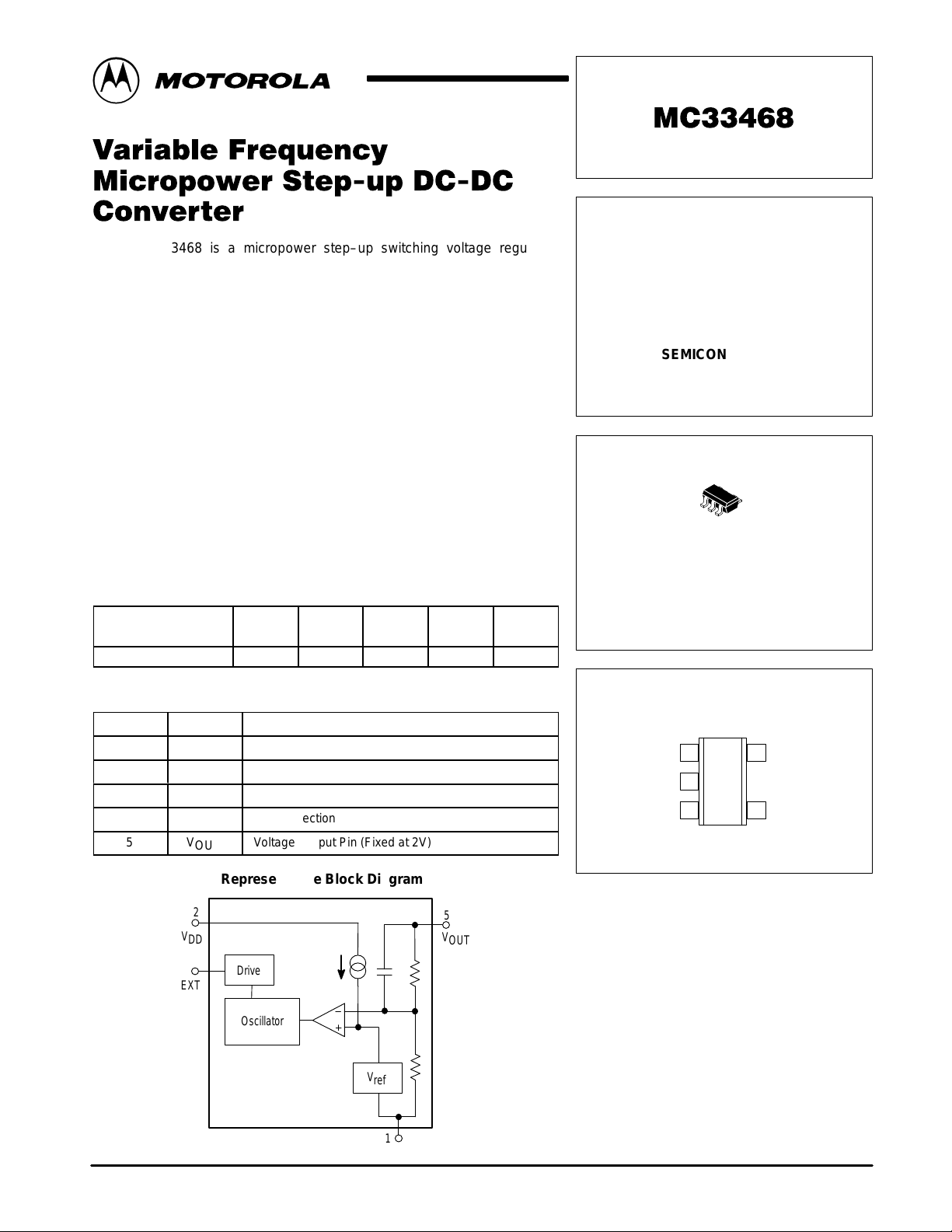
Representative Block Diagram
2
V
DD
3
EXT
Drive
Oscillator
MOTOROLA ANALOG IC DEVICE DATA
5
V
OUT
V
ref
Gnd
1
1
Page 2
MC33468
Á
Á
Á
Á
Á
Á
Á
MAXIMUM RATINGS
Power Supply Voltage (Transient)
Power Supply Voltage (Operating)
External Pin Voltage
EXT Pin Source/Sink Current
(TC = 25°C, unless otherwise noted.)
Rating
Symbol Value Unit
V
V
V
I
DD
DD
EXT
EXT
Power Dissipation and Thermal Characteristics
N Suffix, Plastic Package Case 1212 (SOT–23–5)
Maximum Power Dissipation @ T
Thermal Resistance, Junction–to–Air R
Operating Junction Temperature
Operating Ambient Temperature
Storage Temperature Range
ELECTRICAL CHARACTERISTICS (V
= 250°C P
A
= 1.9 V, TA = 25°C, unless otherwise noted.)
DD
T
θJA
T
T
stg
Characteristic
OSCILLAT OR
Frequency
Oscillator Minimum Supply Voltage (IO = 0 mA)
Oscillator Duty Cycle
EXT OUTPUT
ON State Source Current (V
OFF State Sink Current (V
EXT
EXT
= GND)
= 1.9 V)
TOTAL DEVICE
Output Voltage
Quiescent Bias Current (V
Quiescent Bias Current (V
Internal Resistor (V
OUT
= 1.9 V, IO = 0 mA)
OUT
= 2.1 V, IO = 0 mA)
OUT
to GND)
Output Voltage Temperature Coefficient
I
= 10 mA, –40°C ≤ TA ≤ 85°C
OUT
БББББББББББББББ
1. Indicates test circuits shown on next page.
12
10
–0.3 to VDD + 0.3
50/50
D
150 mW
V
V
V
mA
667 °C/W
J
A
125
–40 to +85
–55 to +125
°C
°C
°C
Symbol Min Typ Max Unit Note
f
osc
V
DD
D
I
source
I
sink
V
OUT
I
Q
I
Q
R
Vout
D
V
OUT
D
T
ÁÁÁ
A
–
–
65
1.5
1.5
1.950
–
–
2.0
–
ÁÁ
180
0.7
75
–
–
2.000
15
3.0
–
±50
ÁÁ
–
0.8
–
–
–
2.050
25
5.0
–
–
ÁÁ
kHz
M
ppm/oc
ÁÁ
V
%
mA
mA
V
µA
µA
1
B
B
B
C
D
A
A
W
E
Á
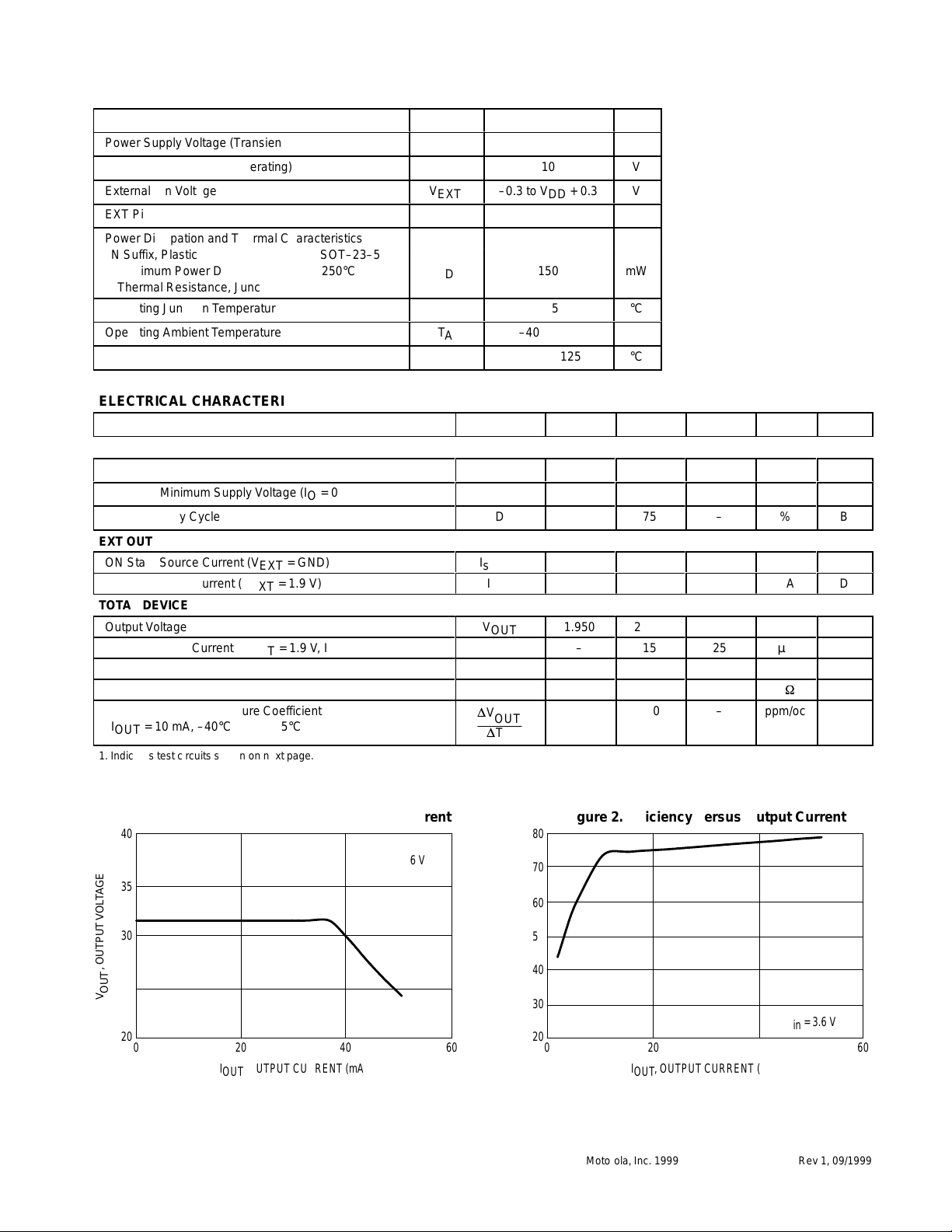
Figure 1. Output Voltage versus Output Current
40
35
30
, OUTPUT VOL TAGE (V)
OUT
25
V
0
I
, OUTPUT CURRENT (mA)
OUT
2
Vin = 3.6 V
Figure 2. Efficiency versus Output Current
80
70
60
50
EFFICIENCY
40
30
2020
0
Motorola, Inc. 1999 Rev 1, 09/1999
Vin = 3.6 V
2020 4040 6060
I
, OUTPUT CURRENT (mA)
OUT
MOTOROLA ANALOG IC DEVICE DATA
Page 3
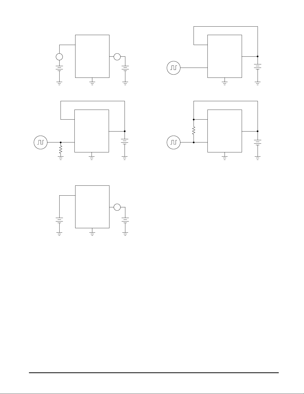
MC33468
A
C
V
DD
GND
GND
V
V
OUT
OUT
A A
EXT
V
DD
EXT
B
Oscilloscope
D
V
DD
EXT
V
DD
EXT
GND
GND
V
OUT
V
OUT
E
V
DD
EXT
GND
V
OUT
A
Figure 3. T est Circuit Schematics
MOTOROLA ANALOG IC DEVICE DATA
3
Page 4

MC33468
DEFINITIONS
Quiescent Bias Current – Current which is used to operate
the switching regulator chip and is not delivered to the load.
Leakage Current – Current drawn through a transistor
junction, under a specified collector voltage, when the
transistor is off.
FUNCTIONAL DESCRIPTION
Introduction
The MC33468 is a monolithic power switching regulator
optimized for dc–to–dc converter applications where power
drain must be minimized. The MC33468 uses Variable
Frequency Modulation to step up the input DC voltage to a
higher accurate output voltage. Potential applications include
low power consumer products and battery powered portable
products. Typical application circuits are shown in Figure 4.
Operating Description
The MC33468 converter operates as a fixed on–time,
variable off–time voltage mode ripple regulator. Operation is
intended to be in the discontinuous mode, where the inductor
current ramps up to a peak value which is greater than or
equal to twice the value of the dc input current during the
on–time of the transistor switch. During the off–time of the
transistor switch, the inductor current ramps down to zero and
remains at zero until another switching cycle begins.
Since the VDD pin is connected to the input no external
startup circuit is needed.
Oscillator
The oscillator frequency, is internally programmed to
180 kHz. The duty ratio of the oscillator is designed for a
constant value of 0.75 nominal. Hence the nominal on–time
of the power switch is:
ton+
f
osc
D
0.75
+
(180 kHz)
+
4.16 µs
Feedback Comparator
The output voltage is sensed and fed to a high speed
comparator noninverting input through an internal resistive
divider. The comparator inverting input is connected to an
internally trimmed reference.
With a voltage mode ripple converter operating under
normal conditions, output switch conduction is initiated and
terminated by the oscillator, off–time is controlled by the high
speed voltage feedback comparator.
Figure 4. T ypical 2.0 V Application with BJT
V
DD
V
IN
EXT
Gnd
V
OUT
Figure 5. Design Equations for Step–Up
Calculation Equation
t
on
L
I
L(avg)
I
L(pk)
V
ripple(pp)
The following converter design characteristics must be chosen:
Vin – Nominal Operating dc input voltage
VO – Desired dc output voltage
IO – Desired dc output current
V
the ripple voltage should be kept to a low value since it directly affects regulation.
Capacitor CO should have a low equivalent series resistance (ESR).
NOTE: 1. V
– Desired peak–to–peak output ripple voltage. For best performance
ripple(pp)
– Saturation voltage of the switching transistor.
sat
n – Estimated circuit efficiency .
(n)(Vin)2(ton)
t
(Vin*
[
D
f
osc
P
O
I
in
V
)(ton)
sat
L
(ton)(IO)
(CO)
V
OUT
4
MOTOROLA ANALOG IC DEVICE DATA
Page 5

MC33468
Figure 6. T ypical 2.0 V Application with MOSFET
V
DD
V
OUT
V
IN
If input voltage is high enough, higher efficiency may be
obtained by using a MOSFET as the switch transistor, in
which no gate resistor or capacitor is needed.
Figure 7. T ypical Application for Output Voltages Over 2.0 V
L1
V
IN
Q1
V
OUT
EXT
GND
MOSFET and BJT voltage rating (VDS and VCE) should be
high enough to allow for spikes in voltage.
D1
R1
V
DD
EXT
V
GND
(2.0 V)
OUT
R2
C
OUT
V
OUT
Inductor (L1) CD54 (15 mH)
Diode (D1) MBRD540T1
Capacitor (C
Transistor (Q1) MMFT3055VL
Resistor (R1) 150 k
Resistor (R2) 10 k
) 47 mF (Tantalum type)
OUT
When choosing the output capacitor, ensure that the
capacitor voltage is higher than V
. Select an inductor with
out
low DC resistance and high saturation. A Schottky diode is
recommended for a lower voltage drop and faster switching.
W
W
Use external resistors that are much smaller resistance than
the resistance internal to the IC (minimum of 2 MW). When R1
is much less than the internal resistance, the error is
minimized.
MOTOROLA ANALOG IC DEVICE DATA
5
Page 6

MC33468
OUTLINE DIMENSIONS
N SUFFIX
PLASTIC PACKAGE
CASE 1212–01
(SOT–23)
ISSUE O
NOTES:
1. DIMENSIONS ARE IN MILLIMETERS.
2. INTERPRET DIMENSIONS AND TOLERANCES
PER ASME Y14.5M, 1994.
3. DATUM C IS A SEATING PLANE.
MILLIMETERS
DIM MIN MAX
A1 0.00 0.10
A2 1.00 1.30
B 0.30 0.50
C 0.10 0.25
D 2.80 3.00
E 2.50 3.10
E1 1.50 1.80
e 0.95 BSC
e1 1.90 BSC
L
0.20 –––
L1 0.45 0.75
A
E
D
1523
B
4
0.05
A2
S
A1
L
E1
L1
B 5X
M
e
0.10 CSBSA
C
C
e1
Recommended Footprint for Surface Mount Applications
1.0
0.7 MAX.
2.4
0.950.95
1.9 (Unit: mm)
SOT–23–5
6
MOTOROLA ANALOG IC DEVICE DATA
Page 7

MC33468
NOTES
MOTOROLA ANALOG IC DEVICE DATA
7
Page 8

MC33468
Motorola reserves the right to make changes without further notice to any products herein. Motorola makes no warranty , representation or guarantee regarding
the suitability of its products for any particular purpose, nor does Motorola assume any liability arising out of the application or use of any product or circuit, and
specifically disclaims any and all liability, including without limitation consequential or incidental damages. “T ypical” parameters which may be provided in Motorola
data sheets and/or specifications can and do vary in different applications and actual performance may vary over time. All operating parameters, including “Typicals”
must be validated for each customer application by customer’s technical experts. Motorola does not convey any license under its patent rights nor the rights of
others. Motorola products are not designed, intended, or authorized for use as components in systems intended for surgical implant into the body, or other
applications intended to support or sustain life, or for any other application in which the failure of the Motorola product could create a situation where personal injury
or death may occur. Should Buyer purchase or use Motorola products for any such unintended or unauthorized application, Buyer shall indemnify and hold Motorola
and its officers, employees, subsidiaries, affiliates, and distributors harmless against all claims, costs, damages, and expenses, and reasonable attorney fees
arising out of, directly or indirectly, any claim of personal injury or death associated with such unintended or unauthorized use, even if such claim alleges that
Motorola was negligent regarding the design or manufacture of the part. Motorola and are registered trademarks of Motorola, Inc. Motorola, Inc. is an Equal
Opportunity/Affirmative Action Employer.
How to reach us:
USA/EUROPE/Locations Not Listed: Motorola Literature Distribution; JAPAN: Motorola Japan Ltd.; SPD, Strategic Planning Office, 141,
P.O. Box 5405, Denver, Colorado 80217. 1–303–675–2140 or 1–800–441–2447 4–32–1 Nishi–Gotanda, Shinagawa–ku, Tokyo, Japan. 81–3–5487–8488
Customer Focus Center: 1–800–521–6274
Mfax: RMFAX0@email.sps.mot.com – TOUCHTONE 1–602–244–6609 ASIA/PACIFIC: Motorola Semiconductors H.K. Ltd.; Silicon Harbour Centre,
Motorola Fax Back System – US & Canada ONLY 1–800–774–1848 2, Dai King Street, Tai Po Industrial Estate, Tai Po, N.T., Hong Kong.
HOME PAGE: http://motorola.com/sps/
8
– http://sps.motorola.com/mfax/ 852–26629298
◊
MOTOROLA ANALOG IC DEVICE DATA
Mfax is a trademark of Motorola, Inc.
MC33468/D
 Loading...