

Datasheet MC33465N-30ATR, MC33465N-45ATR, MC33465N-45CTR, MC33465N-09ATR, MC33465N-09CTR Datasheet (Motorola)
...Page 1
Reset
T
30° t
80°C
SOT–23
Reset
The MC33465 series are micropower undervoltage sensing circuits that
are specifically designed for use with battery powered microprocessor based
systems, where extended battery life is required. A choice of several
threshold voltages from 0.9 V to 4.5 V are available. This device features a
very low quiescent bias current of 1.0 µA typical.
The MC33465 series features a highly accurate voltage reference, a
comparator with precise thresholds and built–in hysteresis to prevent erratic
reset operation, a choice of output configurations between open drain or
complementary, a time delayed output, which can be programmed by the
system designer, and guaranteed operation below 1.0 V with extremely low
standby current. This device is available in a SOT–23 5–pin surface mount
package.
Applications include direct monitoring of the MPU/logic power supply
used in appliance, automotive, industrial and portable equipment.
MC33465 Features:
• Extremely Low Standby Current of 1.0 µA at V
• Wide Input Voltage Range (0.7 V to 10 V)
• Monitors Power Supply Voltages from 1.1 V to 5.0 V
• High Accuracy Detector Threshold (±2.5%)
• Two Reset Output Types (Open Drain or Complementary Drive)
• Programmable Output Delay by External Capacitor (100 ms typ. with
0.15 µF)
• Surface Mount Package (SOT–23 5–Pin)
• Convenient Tape and Reel (3000 per Reel)
= 3.5 V
in
Order this document by MC33465/D
MICROPOWER
UNDERVOLTAGE
SENSING CIRCUITS
WITH PROGRAMMABLE
OUTPUT DELAY
SEMICONDUCTOR
TECHNICAL DATA
5
1
N SUFFIX
PLASTIC PACKAGE
CASE 1212
(SOT–23)
PIN CONNECTIONS
ORDERING INFORMATION
Threshold
Device
MC33465N–09ATR 0.9
MC33465N–20ATR 2.0
MC33465N–27ATR 2.7
MC33465N–30ATR 3.0
MC33465N–45ATR 4.5
MC33465N–09CTR 0.9
MC33465N–20CTR 2.0
MC33465N–27CTR 2.7
MC33465N–30CTR 3.0
MC33465N–45CTR 4.5
Other voltages from 0.9 to 6.0 V , in 0.1 V increments, are available. Consult factory for
information.
This document contains information on a new product. Specifications and information herein
are subject to change without notice.
MOTOROLA ANALOG IC DEVICE DATA
Voltage
Type
Open
Drain
Reset
Compl.
MOS
Reset
Operating
Temperature Range
°
A
= –
o +
°
Package
15
Reset
2
Input
Ground
3
(Top View)
Motorola, Inc. 1996 Rev 0
C
D
N/C
4
1
Page 2
MC33465
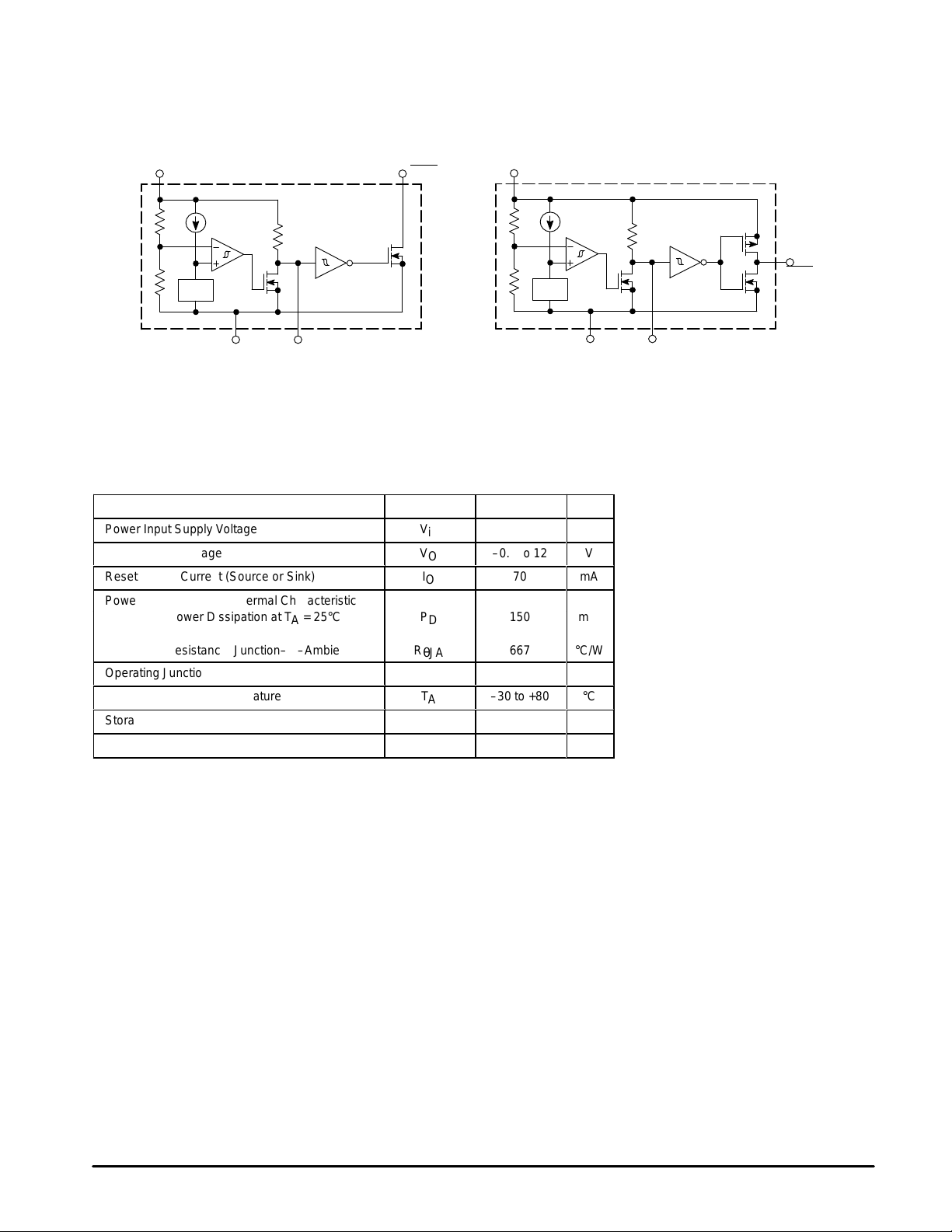
Representative Block Diagrams
MC33465N–YYATR
Open Drain Output Configuration
2 Input
V
ref
3 Gnd 5C
R
D
D
1 Reset
This device contains 28 active transistors.
MAXIMUM RATINGS
Rating Symbol Value Unit
Power Input Supply Voltage
Reset Output Voltage
Reset Output Current (Source or Sink)
Power Dissipation and Thermal Characteristics
Maximum Power Dissipation at TA = 25°C P
Case 1212 (SOT–23) N Suffix
Thermal Resistance, Junction–to–Ambient R
Operating Junction Temperature
Operating Ambient Temperature
Storage Temperature Range
Lead Temperature (Soldering)
Complementary Output Configuration
2 Input
YY Denotes Threshold Voltage
V
V
I
θJA
T
T
T
stg
T
solder
in
O
O
D
J
A
0 to 12
–0.3 to 12
70
150 mW
667 °C/W
+125
–30 to +80
–40 to +125
260°C, 10 s
MC33465N–YYCTR
V
ref
3 Gnd 5C
V
V
mA
°C
°C
°C
R
D
1
Reset
D
2
MOTOROLA ANALOG IC DEVICE DATA
Page 3
MC33465
ÁÁÁ
ÁÁÁ
ÁÁÁ
ÁÁÁ
ÁÁÁ
ÁÁÁ
ÁÁÁ
ÁÁÁ
ÁÁÁ
ELECTRICAL CHARACTERISTICS (For all values T
Characteristic
= 25°C (Note 1), unless otherwise noted.)
A
Symbol Min Typ Max Unit
SENSE COMPARATOR
Threshold Voltage
High to Low State Output (Vin Decreasing) V
IL
09 Suffix 0.878 0.9 0.922
18 Suffix 1.755 1.8 1.845
27 Suffix 2.633 2.7 2.767
36 Suffix 3.51 3.6 3.69
45 Suffix 4.387 4.5 4.612
Threshold Hysteresis (Vin Increasing) V
H
09 Suffix 0.027 0.045 0.063
18 Suffix 0.054 0.09 0.126
27 Suffix 0.081 0.135 0.189
36 Suffix 0.108 0.18 0.252
45 Suffix 0.135 0.225 0.315
Threshold Voltage Temperature Coefficient
T
C
–
±100
RESET OUTPUT
Output Voltage
High State (Complementary Output: I
Low State (Complementary or Open Drain Output: I
Output Sink Current (Vin = 1.5 V, VOL = 0.5 V)
Output Source Current (Vin = 4.5 V, VOH = 2.4 V)
= 1.0 mA) V
source
= 1.0 mA) V
sink
I
I
OH
OH
OL
OL
Vin – 2.1 Vin – 1.0 V
– 0.25 0.5
1.0
1.0
2.0
2.0
DELAY OUTPUT
Output Sink Current (Vin = 1.5 V, VOL = 0.5 V)
Delay Resistance
I
R
OL
0.2
D
0.5
0.8
1.0
TOTAL DEVICE
Operating Input Voltage Range
Quiescent Input Current
V
in
I
in
0.8 to 10
–
Vin = 4.34 V – 5.5 11
Vin = 6.50 V – 1.3 3.9
NOTE: 1.Low duty pulse techniques are used during test to maintain junction temperature as close to ambient as possible.
2.0
V
V
–
PPM/°C
V
in
–
–
–
mA
mA
mA
MΩ
–
V
µA
MOTOROLA ANALOG IC DEVICE DATA
3
Page 4

Figure 1. Reset Low State Sink Current versus
Output Voltage
16
MC33465N–45ATR
14
12
10
8.0
6.0
4.0
, OUTPUT SINK CURRENT (mA)
O
2.0
0
0
TA = 20
°
C
Vin = 2.5 V
2.0 V
1.5 V
0.5
1.0
VOL, LOW STATE OUTPUT VOLTAGE (V)
1.5 2.0
Figure 3. Input Current versus Input Voltage
8.0
MC33465N–45ATR
7.0
µ
6.0
5.0
TA = 25°C
4.0
3.0
, SUPPLY CURRENT ( A) I
2.0
in
I
1.0
0
0
TA = 80°C
TA = –30°C
Vin, INPUT VOLTAGE (V)
80°C
25°C
8.0
2.5
MC33465
3.0
–30°C
10
Figure 2. Output V oltage versus Input Voltage
7.0
MC33465N–45ATR
Ω
Pull–up
470 k
6.0
, OUTPUT VOL TAGE (V)
V
5.0
4.0
3.0
TA = –30°C
1.0
TA = 25°C
TA = 80°C
2.0
Vin, INPUT VOLTAGE (V)
2.0
O
1.0
0
0
3.0
30
°
C
4.0
Figure 4. Comparator Input Threshold Voltage
versus T emperature
3.0
2.9
2.85
2.8
2.75
2.7
, INPUT THRESHOLD VOLTAGE (V)
2.65
in
2.6
–40
V
H
MC33465N–27ATR
–202.0
TA, AMBIENT TEMPERATURE (
VIL + V
H
V
IL
04.0 206.0
40
°
C)
80°C, 20°C
5.0
60
6.0
80
12
MC33465N–27ATR
VOL = 0.5 V
10
8.0
6.0
4.0
, OUTPUT SINK CURRENT (mA)
2.0
O
I
0
0
4
Figure 5. Reset
versus Input V oltage
Vin, INPUT VOLTAGE (V)
Output Sink Current
TA = –30°C
1.5 2.50.5 1.0
2.0
25°C
80°C
3.0
4.0
MC33465N–27CTR
3.5
3.0
2.5
2.0
1.5
1.0
, OUTPUT CURRENT (mA) V
O
I
0.5
0
0
Figure 6. Reset Output Source Current
versus Input V oltage
Vin – VO = 2.1 V
Vin – VO = 1.5 V
Vin – VO = 1.0 V
Vin – VO = 0.5 V
2.0
4.0
Vin, INPUT VOLTAGE (V)
6.0 10
8.0 12
MOTOROLA ANALOG IC DEVICE DATA
Page 5

MC33465
Figure 7. CD Sink Current versus Input Voltage
12
MC33465N–27ATR
VOL = 0.5 V
10
8.0
6.0
4.0
, SINK CURRENT (mA)
D
C
2.0
0
1.8
1.6
Ω
1.4
0.5 1.0 1.5 2.0 3.0
0
Vin, INPUT VOLTAGE (V)
Figure 9. Delay Resistance versus T emperature
TA = –30°C
25°C
80°C
2.5
Figure 8. CD Sink Current versus CD Voltage
16
14
12
10
8.0
6.0
, SINK CURRENT (mA)
4.0
sink
I
2.0
0
0
Figure 10. Detector Threshold versus T emperature
1.9
1.8
1.7
0.5 1.0 1.5 2.0 3.0
Vin = 2.5 V
Vin = 2.0 V
Vin = 1.5 V
2.5
VCD, VOLTAGE (V)
1.2
1.0
0.8
, DELAY RESISTANCE (M )
D
0.6
R
0.4
–40
–20 0 20 40 80
TA, AMBIENT TEMPERATURE (
60
°
C)
Figure 11. Output Delay T ime versus
1000
, OUTPUT DELA Y TIME (ms)
p
t
100
tD: Output Switch
Low to High
10
1.0
0.1
Delay Capacitance
1.6
1.5
1.4
1.3
, DETECTOR THRESHOLD VOLTAGE (V)
th(D)
1.2
V
tD: Output Switch
High to Low
Vin = 2.97 V
MC33465N–27ATR
–40
–20 0 20 40 80
TA, AMBIENT TEMPERATURE (°C)
60
0.01
0.0001
MOTOROLA ANALOG IC DEVICE DATA
0.001 0.01 0.1
µ
CD, DELAY CAPACITANCE (
F)
5
Page 6
MC33465
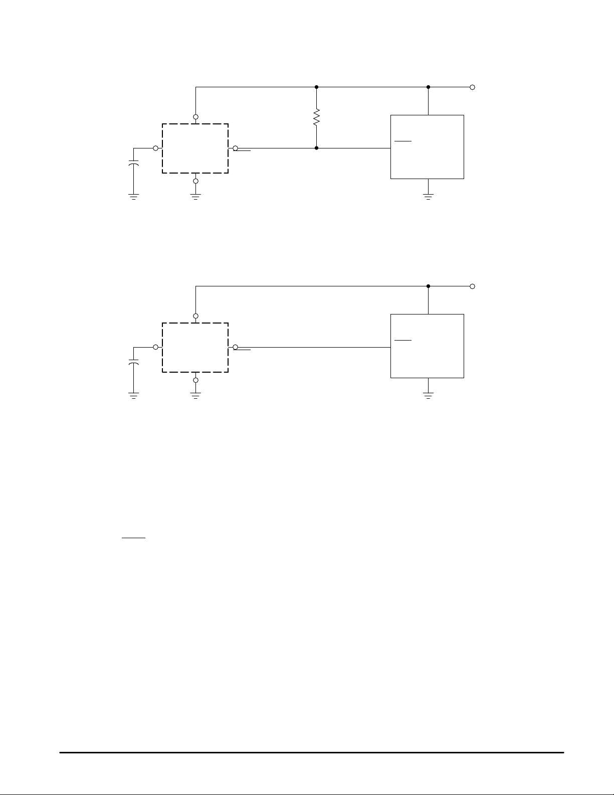
Figure 12. T ypical Open Drain Application
V
DD
2 Input
5
MC33465
C
C
D
Series
D
Gnd
3
1
Reset
R
Reset
V
DD
Gnd
CPU
Figure 13. T ypical Complementary Output Application
V
DD
2 Input
5
MC33465
C
C
D
Series
D
3
Gnd
1
Reset
Reset
V
DD
Gnd
CPU
APPLICATION CIRCUIT INFORMATION
The MC33465 series are micropower undervoltage
sensing circuits which offer a programmable time delayed
output with the choice of either complementary output drive
or open drain output configurations. Figure 14 shows the
timing relationships between the input voltage and the
resulting circuit waveforms. When the input voltage (Vin)
exceeds the sense comparator threshold, the timing
capacitor
resistor. When the output inverting driver threshold is
exceeded, the Reset
is allowed to charge through the internal delay
output switches from a logic “0” to a
logic “1”. The top curve of Figure 11 provides the nominal
delay time for a given value of delay capacitance. When V
drops below the comparator threshold minus hysteresis
voltage, the delay capacitor discharges. When the
capacitance voltage drops below the inverting drive
threshold, the output switches from a logic “1” to a logic “0”.
The bottom curve in Figure 1 1 provides typical delay time for
given delay capacitance values. The inverting driver
threshold voltage is typically about Vin/2, as shown in
Figure 10.
in
6
MOTOROLA ANALOG IC DEVICE DATA
Page 7

Input Voltage
Delay Capacitor
Reset
Output
VIL + V
V
MC33465
Figure 14. Timing Waveforms
V
in
H
IL
V
in
0 V
t
D
L–H L–H
t
D
H–L
t
D
t
D
H–L
MOTOROLA ANALOG IC DEVICE DATA
7
Page 8

MC33465
OUTLINE DIMENSIONS
N SUFFIX
PLASTIC PACKAGE
CASE 1212–01
(SOT–23)
ISSUE O
NOTES:
1. DIMENSIONS ARE IN MILLIMETERS.
2. INTERPRET DIMENSIONS AND TOLERANCES
PER ASME Y14.5M, 1994.
3. DATUM C IS A SEATING PLANE.
MILLIMETERS
DIM MIN MAX
A1 0.00 0.10
A2 1.00 1.30
B 0.30 0.50
C 0.10 0.25
D 2.80 3.00
E 2.50 3.10
E1 1.50 1.80
e 0.95 BSC
e1 1.90 BSC
L
0.20 –––
L1 0.45 0.75
A
E
D
1523
B
4
0.05
A2
S
A1
L
E1
L1
B 5X
M
e
0.10 CSBSA
C
C
e1
Motorola reserves the right to make changes without further notice to any products herein. Motorola makes no warranty , representation or guarantee regarding
the suitability of its products for any particular purpose, nor does Motorola assume any liability arising out of the application or use of any product or circuit, and
specifically disclaims any and all liability, including without limitation consequential or incidental damages. “T ypical” parameters which may be provided in Motorola
data sheets and/or specifications can and do vary in different applications and actual performance may vary over time. All operating parameters, including “Typicals”
must be validated for each customer application by customer’s technical experts. Motorola does not convey any license under its patent rights nor the rights of
others. Motorola products are not designed, intended, or authorized for use as components in systems intended for surgical implant into the body, or other
applications intended to support or sustain life, or for any other application in which the failure of the Motorola product could create a situation where personal injury
or death may occur. Should Buyer purchase or use Motorola products for any such unintended or unauthorized application, Buyer shall indemnify and hold Motorola
and its officers, employees, subsidiaries, affiliates, and distributors harmless against all claims, costs, damages, and expenses, and reasonable attorney fees
arising out of, directly or indirectly, any claim of personal injury or death associated with such unintended or unauthorized use, even if such claim alleges that
Motorola was negligent regarding the design or manufacture of the part. Motorola and are registered trademarks of Motorola, Inc. Motorola, Inc. is an Equal
Opportunity/Affirmative Action Employer.
How to reach us:
USA/EUROPE/Locations Not Listed: Motorola Literature Distribution; JAPAN: Nippon Motorola Ltd.; Tatsumi–SPD–JLDC, 6F Seibu–Butsuryu–Center,
P.O. Box 5405, Denver, Colorado 80217. 303–675–2140 or 1–800–441–2447 3–14–2 Tatsumi Koto–Ku, Tokyo 135, Japan. 81–3–3521–8315
Mfax: RMFAX0@email.sps.mot.com – TOUCHTONE 602–244–6609 ASIA/P ACIFIC: Motorola Semiconductors H.K. Ltd.; 8B Tai Ping Industrial Park,
INTERNET: http://Design–NET .com 51 Ting Kok Road, Tai Po, N.T., Hong Kong. 852–26629298
8
◊
MOTOROLA ANALOG IC DEVICE DATA
Mfax is a trademark of Motorola, Inc.
MC33465/D
 Loading...