

Page 1
Semiconductor Components Industries, LLC, 2000
April, 2000 – Rev. 1
1 Publication Order Number:
MC33441/D
MC33441
Electroluminescent Lamp
Driver IC
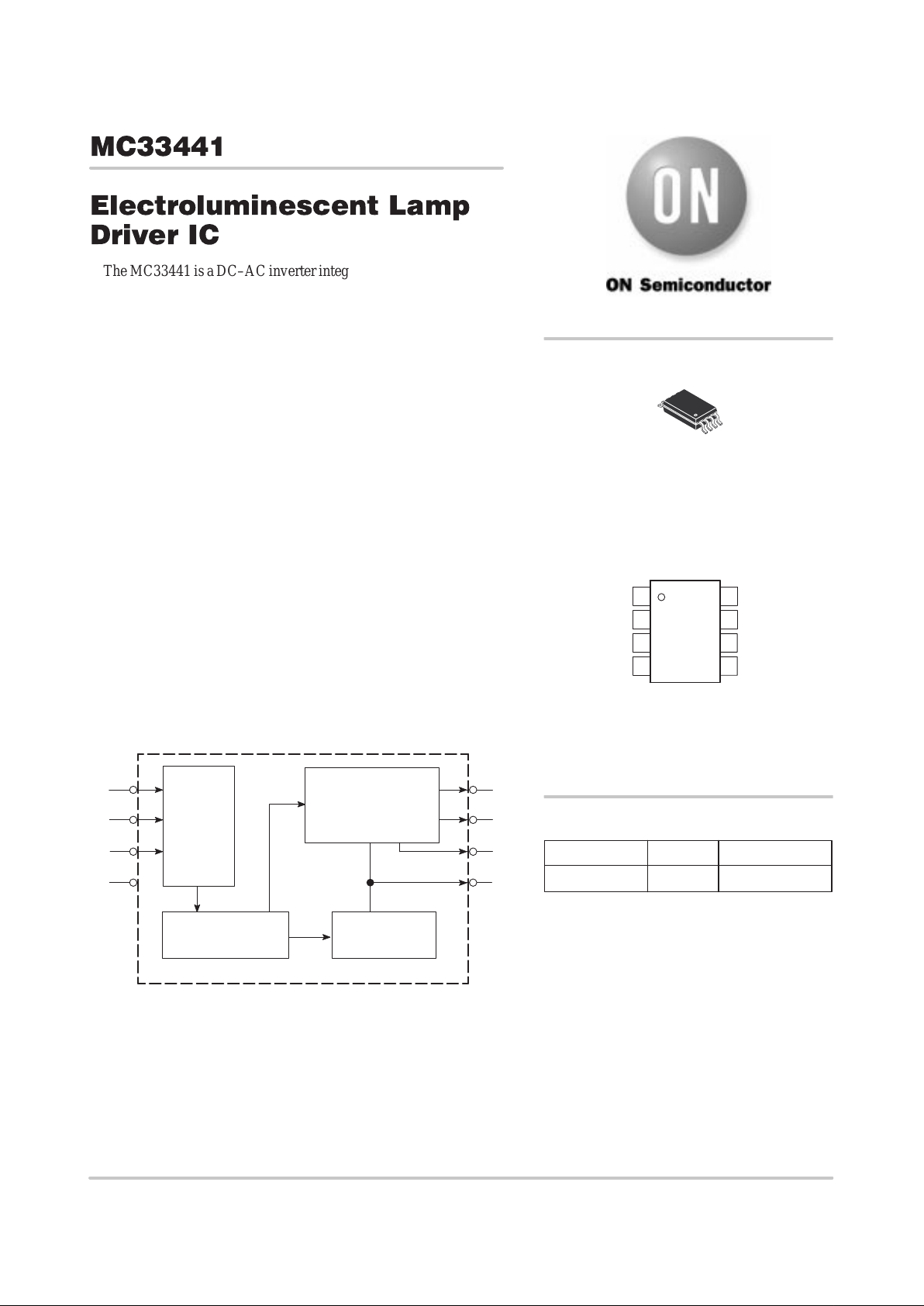
The MC33441 is a DC–AC inverter integrated circuit for driving EL
lamps. It can boost the supply voltage to the level required by EL
lamps and also provide high voltage AC lamp excitation. It consists of
an oscillator, a frequency divider , a coil driving circuit and a switched
H–bridge network. The input supply voltage range is from 1.8V to
3.5V and is capable to supply a typical 140Vpp AC output voltage.
The standby current of the device is typically 10nA which is ideal for
low power portable products. Externally, one inductor and one resistor
are needed to generate the desirable voltage charge and to fine tune the
oscillator’s frequency. This device is offered in 8–Pin TSSOP
miniature package. The operating temperature is –20°C to 70°C.
Features:
• Battery Operation 1.8V – 3.5V
• Typical Voltage Output 140Vpp
• Typical Standby Current 10nA
• Internal Oscillator with External Tuning Resistor
• Enable Control Pin with a 300K Internal Pull–Down Resistor
• 8–Pin TSSOP Package (Thickness = 1.05mm, Width = 4.5mm,
Length = 3.1mm & Lead Pitch = 0.65mm)
Types of Applications:
• Pagers, Cellular Phones, Portable CD Players/Minidisks
• Databanks, Calculators
Simplified Block Diagram
FREQUENCY
DIVIDER
VDD
ENB
RT1
OSC
F
EL
VSS
1
2
3
4
H–BRIDGE
COIL
DRIVER
F
COIL
EL1
EL2
FILTER
COIL
8
7
6
5
Device Package Shipping
ORDERING INFORMATION
MC33441DTBR2 TSSOP–8 2500 Units / Reel
TSSOP–8
DTB SUFFIX
CASE 948J
http://onsemi.com
8
1
PIN CONNECTIONS AND
MARKING DIAGRAM
4
3
VSS COIL
FILTER
5
6
(Top View)
ENB
RT1
1
VDD
EL2
EL1
7
8
2
M33
441
ALY
W
A = Assembly Location
L = Wafer Lot
Y = Y ear
W = Work Week
Page 2
MC33441
http://onsemi.com
2
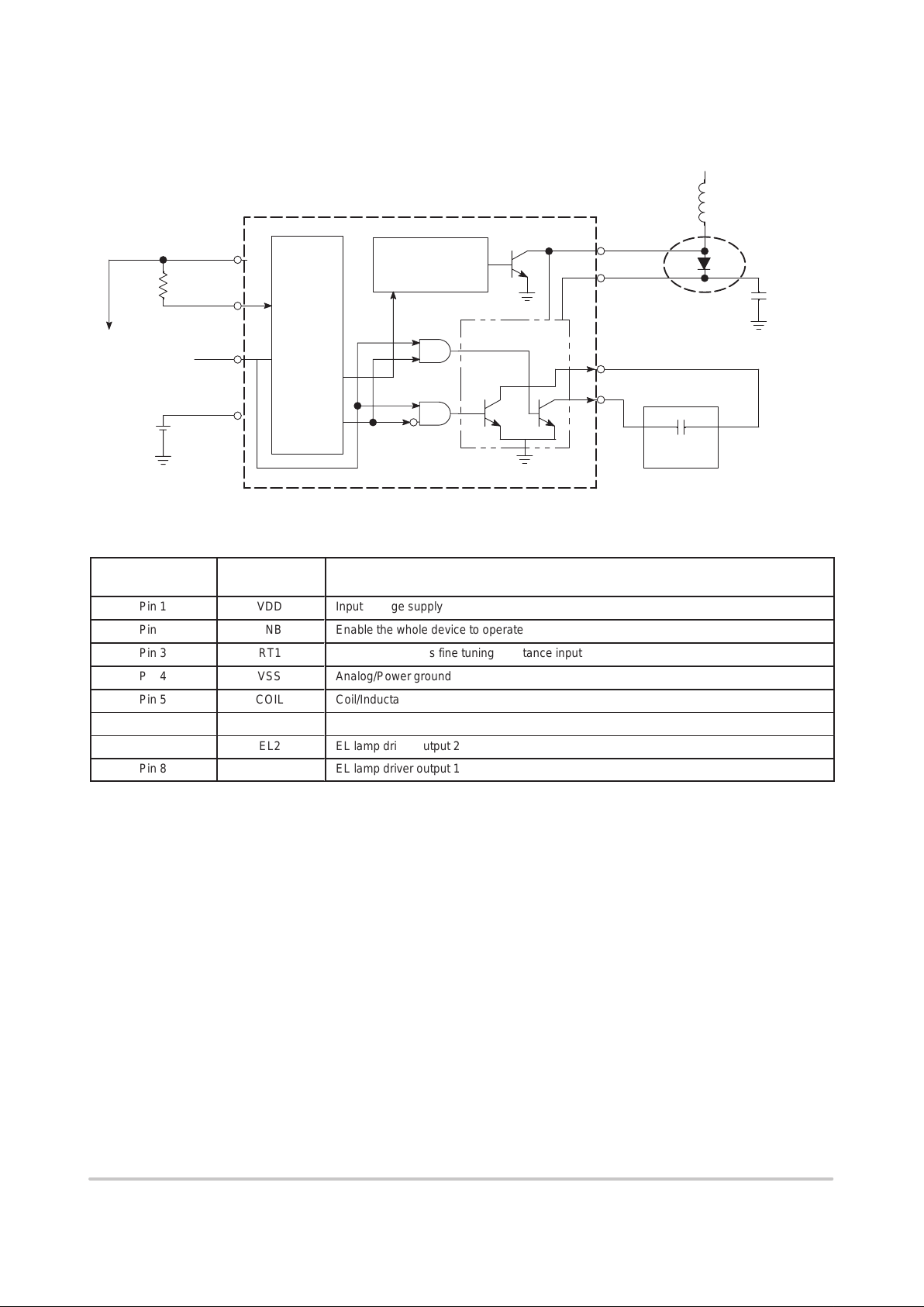
Figure 1. Test Circuit
H–BRIDGE
VSS
ENB
RT1
OSC
&
FREQ.
DIVIDER
F
EL
VDD
1
2
3
4
COIL DRIVER
EL LAMP
AND2
EL1
EL2
FILTER
COIL
8
7
6
5
F
COIL
AND2
AND2
INDUCTOR
C
FILTER
R
EXT
Battery / V
DD
OPTIONAL
MAIN SWITCH
PIN FUNCTION DESCRIPTION
Pin No.
(TSSOP–8)
Name Description
Pin 1
VDD
ББББББББББББББББББББББ
Input voltage supply
Pin 2
ENB
ББББББББББББББББББББББ
Enable the whole device to operate
Pin 3
RT1
ББББББББББББББББББББББ
Internal oscillator’s fine tuning resistance input
Pin 4
VSS
ББББББББББББББББББББББ
Analog/Power ground
Pin 5
COIL
ББББББББББББББББББББББ
Coil/Inductance input
Pin 6
Filter
ББББББББББББББББББББББ
EL Filter
Pin 7
EL2
ББББББББББББББББББББББ
EL lamp driver output 2
Pin 8
EL1
ББББББББББББББББББББББ
EL lamp driver output 1
Page 3
MC33441
http://onsemi.com
3
MAXIMUM RATINGS (T
C
= 25°C, unless otherwise noted.)
Rating
Symbol Max Unit
Power Supply Voltage
V
DD
7.5
V
ББББББББББББ
Á
Digital Input Voltage Range
ÁÁ
Á
LOGIC = 0
LOGIC = 1
ÁÁÁ
Á
0.5
V
DD
Á
Á
V
Operating Junction Temperature
T
J(max)
150
°C
Operating Ambient Temperature
T
A
–20 to +70
°C
Storage Temperature Range
T
stg
–50 to +150
°C
Power Dissipation
P
D
300
mW
Thermal Resistance, Junction–to–Air
R
θJA
178
°C/W
DC ELECTRICAL CHARACTERISTICS (V
DD
= 2.65V , TA = 25°C, Lamp Capacitance = 2.2nF, Coil = 1mH unless
otherwise noted.)
Characteristic
Symbol Min Typ Max Unit
Supply Voltage
V
DD
1.8
–
3.5
V
Output Voltage (1.8V < VDD ≤ 3.5 V)
V
EL
120
140
160
V
Peak Coil Current (1.8V < VDD ≤ 3.5 V)
I
COIL
–
70
150
mA
Average Coil Current from Battery (1.8V < VDD ≤ 3.5 V)
I
VDD
–
35
75
mA dc avg
Standby Current (VDD = 3.0 V, ENB = 0)
I
STAND
–
10
100
nA
Clock Frequency (R
EXT
= 125KW)
F
osc
112
140
168
kHz
Lamp Drive Frequency (F
osc
Divide by 384)
F
EL
–
364.6
–
Hz
Coil Drive Frequency ( F
osc
Divide by 4)
F
COIL
–
35
–
kHz
Coil Drive Clock Duty Cycle
DC
COIL
–
75
–
%
EL Lamp Capacitance Range
C
EL
–
2.2
–
nF
V
EL1
TIME
V
EL2
V
EL
TIME
TIME
Typical Vpp = 140V
(160V max)
Figure 2. Output Waveform
Page 4
MC33441
http://onsemi.com
4
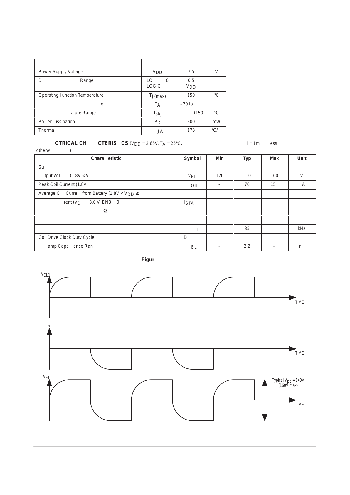
Figure 3. Output Waveform vs. Time
VDD = 2.65V
Lamp Freq. = 365Hz
EL Lamp = 2.2nF
X = 1ms/div, Y = 50V/div
OPERA TING DESCRIPTION
General
The MC33441 is a DC–AC inverter integrated circuit for
driving EL lamps. It can boost the supply voltage to the level
required by EL lamps and also provide high voltage AC lamp
excitation. It consists of an oscillator, a frequency divider, a coil
driving circuit and a switched H–bridge network. The input
supply voltage range is from 1.8V to 3.5V and is capable to
supply a typical 140Vpp AC output voltage. The standby
current of the device is typically 10nA which is ideal for low
power portable products. Externally, one inductor and one
resistor are needed to generate the desirable voltage charge and
to fine tune the oscillator’s frequency. This device is offered in
8–Pin TSSOP packages. The operating temperature is –20°C to
70°C.
Oscillator and Frequency Divider
Two circuits are put together to form the oscillator. They are
Vref and Ibias. The functionality of Vref block is to generate a
zero temperature coefficient (TC) voltage reference which is
about 1.27V. This 1.27V will then be used in Ibias circuit to
provide current biasing to all of the internal circuits with the
value equal to Vref divided by an internal resistor. Besides of
that, an external resistor is also connected to this circuit block for
setting the oscillator’s frequency. The temperature coefficient is
dominated by the value of that resistor. Therefore, if a low TC
resistor is used, the oscillator frequency’s TC can be kept low.
The current mirrors with the induced current equal to the Vref
divided by an external resistor are used to charge and discharge
an internal capacitor to provide a 50% duty cycle clock signal.
This original clock pulse will then be fed into the frequency
divider which will generate two additional clock signals with
different frequency and duty cycle to the coil–driver and the
H–bridge circuits. The oscillator frequency is governed by the
following equation:
F
OSC
+
ǒ
1
6 R
EXT
C
INT
HzǓ+
1.667 10
10
R
EXT
Hz
F
COIL
= F
OSC
B 4
FEL = F
OSC
B 384
where C
INT
is about 10pF.
Coil Driver
The coil driver is basically a simplified boost converter. It
takes a higher frequency clock signal from the frequency divider
to turn on/off the main switch alternatively. When the main
switch is on, current will flow through the coil to ground. Once
the switch is being turned off, the energy stored in the coil will
be released to the external capacitor (EL lamp) through an
internal diode. According to the frequency of the clock signals
between the coil driver and the H–bridge, the external capacitor
(EL lamp) will be charging to the desirable level.
Current limit circuit (typical 70mA & max. 150mA) is
implemented in this device. Since the current through the coil
will increase corresponding to the input voltage, if the input
voltage is high and the inductance of the coil is small, the coil
can be saturated. The current limit feature is used to avoid this
happen. The main switch is parallel to a much smaller switch
which has their collector and their base connected together.
However, the emitter of the smaller switch is tied to a sensing
resistor while the emitter of the main switch is connected to
ground. The coil current will split into two according to the
sizing ratio between the main and the smaller switch. The
current through the smaller switch will also flow through the
sensing resistor and generates a voltage. If the voltage across this
sensing resistor is above the pre–set value, then both switches
Page 5

MC33441
http://onsemi.com
5
will be turned off and the energy will release to the EL lamp.
And, those switches will remain off until the next clock cycle.
H–Bridge Network
To achieve the 140V peak–to–peak voltage, H–bridge
network is used to charge and discharge the EL lamp. The
switching frequency of the bridge network is controlled by a
clock signal from the divider with its frequency much lower than
the one to the coil–driver. Moreover, to reduce the current
consumption, the biasing current to the two low–side switches
of the H–bridge is not activated until the coil–driver circuit
needed to release the energy to the EL lamp. Then, the biasing
circuit will be on and be ready before the main switch in the
coil–driver really starts to turn off.
External Components
System designer will base on the application to decide the size
and the type of the EL lamp to be used. The external resistance
(R
EXT
) at RT1 pin determines the excitation frequency (FEL) for
the lamp. The relationship between R
EXT
and the frequency is:
FEL = F
OSC
B 384
By substitute the equation of F
OSC
from Oscillator &
Frequency Divider.
FEL+
4.341 10
7
R
EXT
Hz
so
R
EXT
+
4.341 10
7
F
EL
W
Moreover, if a low TC resistor is used, the oscillator
frequency’s TC can be kept low. The filter capacitor is to provide
a smooth and more stable output waveform for the EL lamp.
The value of this capacitor depends on the input voltage and the
coil’s inductance value. Equations below can be used to estimate
filter capacitor’s value at different input voltage.
Best Case Approximation for the Filter Capacitor:
C
FILTER
+
0.026 (Vin*
VSW)
2
ń(L
F
OSC
2
)
Worst Case Approximation for the Filter Capacitor:
C
FILTER
+
0.085 (Vin*
VSW)
2
ń(L
F
OSC
2
)
where VIN is the input voltage, VSW is voltage across the
switch when it is on, L is the coil’s value and F
OSC
is the
clock frequency.
Measurement below is recorded with the condition: coil
= 1mH, EL lamp = 2.2nF and at room temperature.
Table 1: Reference for C
FILTER
VDD R
EXT
C
FILTER
1.8V
100K–130K
W
5n–10nF
2.0V
100K–130K
W
10n–22nF
2.5V
100K–130K
W
10n–22nF
3.0V
100K–130K
W
22nF–33nF
Page 6

MC33441
http://onsemi.com
6
TYPICAL OPERATING CHARACTERISTICS
Figure 4. Oscillator Frequency vs. R
EXT
Figure 5. Lamp Frequency vs. R
EXT
Figure 6. Current Consumption vs. Coil Inductance Figure 7. Current Consumption vs. V
DD
Figure 8. Output Voltage vs. R
EXT
Figure 9. Output Voltage vs. Coil Inductance
COIL INDUCTANCE (mH)
LAMP FREQ. (Hz)
VOUT (V)
R
EXT
(OHM)
0
50
100
150
250
200K
300
200
50K 75K 100K 150K
VDD = 2.65V
Coil = 1mH
EL lamp = 2.2nF
OSC. FREQ. (KHz)
COIL INDUCTANCE (mH)
I (mA)
R
EXT
(OHM)
VOUT (V)
VDD (V)
I (mA)
R
EXT
(OHM)
0
100
200
300
500
200K
600
400
50K 75K 100K 150K
VDD = 2.65V
Coil = 1mH
EL lamp = 2.2nF
7
00
0
5
10
15
25
1.47
20
0.56 0.82 1 1.33
VDD = 2.65V
Lamp Freq. = 365Hz
EL lamp = 2.2nF
0
5
10
15
25
3.5
30
20
1.8 2 2.65 3
Coil = 1mH
Lamp Freq. = 365Hz
EL Lamp = 2.2nF
120
122
124
126
130
200K
132
128
50K 75K 100K 150K
VDD = 2.65V
Coil = 1mH
EL Lamp = 2.2nF
134
136
138
110
115
120
125
135
1.47
130
0.56 0.82 1 1.33
VDD = 2.65V
Lamp Freq. = 365Hz
EL Lamp = 2.2nF
140
145
150
Page 7

MC33441
http://onsemi.com
7
APPLICATION INFORMA TION
EL Lamp Selection
EL lamps are a laminate which exhibit a capacitance on
the order of 2.5nF to 3.5nF per square inch. The light will
emit as the high voltage is applied across the electrodes of
this capacitance. The color of the emitted light is determined
by the type of chemical used and the frequency of the
excitation voltage. On the other hand, the lamp brightness
increases approximately the square of the applied voltage
and nearly linear to the excitation frequency. Once a lamp
has been selected, the operating frequency and the essential
voltage for the optimum performance is determined. Then,
the driver circuit can begin to design.
Inductor Selection (L1)
Use a 1mH/0.15A inductor for MC33441. Higher
inductor values can be used to reduce the peak transient coil
current from the battery supply. As the value of the inductor
(L1), increases, the resistor (R1) value may need to increase
correspondingly to provide optimum performance. While a
lower inductor values lead to smaller physical size, it will
generate a higher peak coil current. A lower resistor (R1)
value should be used when a lower inductance coil is being
used.
The inductor must have a saturation current rating equal
to or bigger than the peak coil current which is 150mA.
Filter Capacitor Selection (C2)
See Table 1 for the estimated value of the filter capacitors
based on the input voltage supply. Since the maximum
voltage of the filter capacitor can reach 70V or even 80V,
capacitor with high voltage rating will be required.
Resistor Selection (R1)
Since the fundamental frequency of the oscillator is set by
the external resistor (R1), the temperature coefficient of the
frequency is dominated by the value of this resistor. A low
temperature coefficient (TC) resistor is suggested to use for
keeping the variation of oscillator’s frequency low against the
operation temperature range. (See Page 4, Fig. 3 & Fig. 4)
R1+R
EXT
+
4.341 10
7
F
EL
W
Layout
The MC33441 is high output voltage operation make PC
board layout critical to minimize ground bounce and noise.
Locate input bypass capacitor, filter capacitor and
oscillator’s resistor as close to the device pins as possible.
Figure 10. MC33441 Demo Board Schematic
MC33441
VDD
(TSSOP–8)
C1
0.1µF
L1
1mH
ENABLE
R1
130K
ENB
RT1
VSS
EL1
EL2
FILTER
COIL
EL–LAMP
1
2
3
4
8
7
6
5
BATTERY
PB1
C2
27nF/100V
U1
COMPONENT SUPPLIER
Supplier Part Number Description Phone
ББББББББ
Á
Tech–Wave Industrial Co., Ltd.
БББББ
Á
Part# CC–0012
ББББББББББ
Á
EL–Lamp: 14.5mm x 47mm Color:
Y ellow–Green
БББББ
Á
(886)–2–22692827
ББББББББ
Á
Coils Electronics Co., Ltd.
БББББ
Á
Part# CRCH664–
102K–831015
ББББББББББ
Á
Inductor: 1mH / 0.15A
БББББ
Á
(852)–2341–5539
Page 8

MC33441
http://onsemi.com
8
Figure 11. MC33441 PC Board – Top View
Figure 12. MC33441 Component Placement Guide – Component Side
Figure 13. MC33441 PC Board – Bottom View
Page 9

MC33441
http://onsemi.com
9
P ACKAGE DIMENSIONS
TSSOP–8
DTB SUFFIX
CASE 948J–01
ISSUE O
DIM MIN MAX MIN MAX
INCHESMILLIMETERS
A 2.90 3.10 0.114 0.122
B 4.30 4.50 0.169 0.177
C ––– 1.20 ––– 0.047
D 0.05 0.15 0.002 0.006
F 0.50 0.75 0.020 0.030
G 0.65 BSC 0.026 BSC
H 0.50 0.60 0.020 0.024
J 0.09 0.20 0.004 0.008
J1 0.09 0.16 0.004 0.006
K 0.19 0.30 0.007 0.012
K1 0.19 0.25 0.007 0.010
L 6.40 BSC 0.252 BSC
M 0 8 0 8
NOTES:
1. DIMENSIONING AND TOLERANCING PER ANSI
Y14.5M, 1982.
2. CONTROLLING DIMENSION: MILLIMETER.
3. DIMENSION A DOES NOT INCLUDE MOLD
FLASH. PROTRUSIONS OR GATE BURRS. MOLD
FLASH OR GATE BURRS SHALL NOT EXCEED
0.15 (0.006) PER SIDE.
4. DIMENSION B DOES NOT INCLUDE
INTERLEAD FLASH OR PROTRUSION.
INTERLEAD FLASH OR PROTRUSION SHALL NOT
EXCEED 0.25 (0.010) PER SIDE.
5. DIMENSION K DOES NOT INCLUDE DAMBAR
PROTRUSION. ALLOWABLE DAMBAR
PROTRUSION SHALL BE 0.08 (0.003) TOTAL IN
EXCESS OF THE K DIMENSION AT MAXIMUM
MATERIAL CONDITION.
6. TERMINAL NUMBERS ARE SHOWN FOR
REFERENCE ONLY.
7. DIMENSION A AND B ARE TO BE
DETERMINED AT DATUM PLANE –W–.
____
SECTION N–N
SEATING
PLANE
IDENT.
PIN 1
1
4
8
5
SEE DETAIL E
J
J1
B
C
D
A
K
K1
H
G
DETAIL E
F
M
L
2X L/2
–U–
S
U0.15 (0.006) T
S
U0.15 (0.006) T
S
U
M
0.10 (0.004) V
S
T
0.10 (0.004)
–T–
–V–
–W–
0.25 (0.010)
8x REFK
N
N
Page 10

MC33441
http://onsemi.com
10
Notes
Page 11

MC33441
http://onsemi.com
11
Notes
Page 12
MC33441
http://onsemi.com
12
ON Semiconductor and are trademarks of Semiconductor Components Industries, LLC (SCILLC). SCILLC reserves the right to make changes
without further notice to any products herein. SCILLC makes no warranty , representation or guarantee regarding the suitability of its products for any particular
purpose, nor does SCILLC assume any liability arising out of the application or use of any product or circuit, and specifically disclaims any and all liability ,
including without limitation special, consequential or incidental damages. “Typical” parameters which may be provided in SCILLC data sheets and/or
specifications can and do vary in different applications and actual performance may vary over time. All operating parameters, including “Typicals” must be
validated for each customer application by customer’s technical experts. SCILLC does not convey any license under its patent rights nor the rights of others.
SCILLC products are not designed, intended, or authorized for use as components in systems intended for surgical implant into the body, or other applications
intended to support or sustain life, or for any other application in which the failure of the SCILLC product could create a situation where personal injury or
death may occur. Should Buyer purchase or use SCILLC products for any such unintended or unauthorized application, Buyer shall indemnify and hold
SCILLC and its officers, employees, subsidiaries, affiliates, and distributors harmless against all claims, costs, damages, and expenses, and reasonable
attorney fees arising out of, directly or indirectly , any claim of personal injury or death associated with such unintended or unauthorized use, even if such claim
alleges that SCILLC was negligent regarding the design or manufacture of the part. SCILLC is an Equal Opportunity/Affirmative Action Employer .
PUBLICATION ORDERING INFORMATION
CENTRAL/SOUTH AMERICA:
Spanish Phone: 303–308–7143 (Mon–Fri 8:00am to 5:00pm MST)
Email: ONlit–spanish@hibbertco.com
ASIA/PACIFIC : LDC for ON Semiconductor – Asia Support
Phone: 303–675–2121 (Tue–Fri 9:00am to 1:00pm, Hong Kong Time)
T oll Free from Hong Kong & Singapore:
001–800–4422–3781
Email: ONlit–asia@hibbertco.com
JAPAN: ON Semiconductor, Japan Customer Focus Center
4–32–1 Nishi–Gotanda, Shinagawa–ku, T okyo, Japan 141–8549
Phone: 81–3–5740–2745
Email: r14525@onsemi.com
ON Semiconductor Website: http://onsemi.com
For additional information, please contact your local
Sales Representative.
MC33441/D
NORTH AMERICA Literature Fulfillment:
Literature Distribution Center for ON Semiconductor
P.O. Box 5163, Denver, Colorado 80217 USA
Phone: 303–675–2175 or 800–344–3860 T oll Free USA/Canada
Fax: 303–675–2176 or 800–344–3867 Toll Free USA/Canada
Email: ONlit@hibbertco.com
Fax Response Line: 303–675–2167 or 800–344–3810 T oll Free USA/Canada
N. American Technical Support: 800–282–9855 Toll Free USA/Canada
EUROPE: LDC for ON Semiconductor – European Support
German Phone: (+1) 303–308–7140 (M–F 1:00pm to 5:00pm Munich Time)
Email: ONlit–german@hibbertco.com
French Phone: (+1) 303–308–7141 (M–F 1:00pm to 5:00pm Toulouse T ime)
Email: ONlit–french@hibbertco.com
English Phone: (+1) 303–308–7142 (M–F 12:00pm to 5:00pm UK Time)
Email: ONlit@hibbertco.com
EUROPEAN TOLL–FREE ACCESS*: 00–800–4422–3781
*Available from Germany, France, Italy , England, Ireland
 Loading...