

Page 1
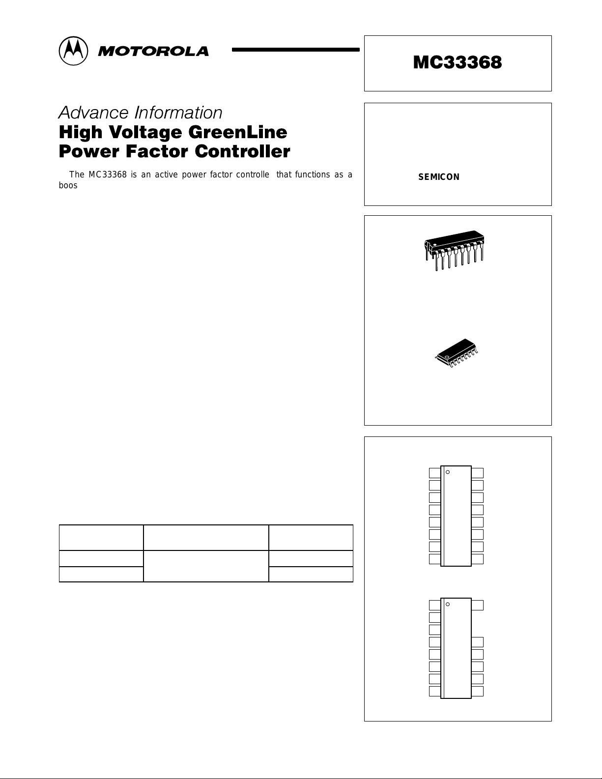
Order this document by MC33368/D
T
25° to +125°C
The MC33368 is an active power factor controller that functions as a
boost preconverter in off–line power supply applications. MC33368 is
optimized for low power, high density power supplies requiring a minimum
board area, reduced component count and low power dissipation. The
narrow body SOIC package provides a small footprint. Integration of the high
voltage startup saves approximately 0.7 W of power compared to resistor
bootstrapped circuits.
The MC33368 features a watchdog timer to initiate output switching, a
one quadrant multiplier to force the line current to follow the instantaneous
line voltage a zero current detector to ensure critical conduction operation, a
transconductance error amplifier, a current sensing comparator, a 5.0 V
reference, an undervoltage lockout (UVLO) circuit which monitors the V
supply voltage and a CMOS driver for driving MOSFET s. The MC33368 also
includes a programmable output switching frequency clamp. Protection
features include an output overvoltage comparator to minimize overshoot, a
restart delay timer and cycle–by–cycle current limiting.
• Lossless Off–Line Startup
• Output Overvoltage Comparator
• Leading Edge Blanking (LEB) for Noise Immunity
• Watchdog T imer to Initiate Switching
CC
HIGH VOLTAGE
GREENLINE POWER
FACTOR CONTROLLER
SEMICONDUCTOR
TECHNICAL DATA
16
1
P SUFFIX
PLASTIC PACKAGE
CASE 648
(DIP–16)
16
1
D SUFFIX
PLASTIC PACKAGE
CASE 751K
(SO–16)
• Restart Delay Timer
GreenLine is a trademark of Motorola, Inc.
ORDERING INFORMATION
Operating
Device
MC33368D
MC33368P
Temperature Range
–
= –
J
PIN CONNECTIONS
5.0 V
Restart Delay
Voltage FB
Package
°
°
SO–16
DIP–16
Current Sense
Zero Current
5.0 V
Restart Delay
Voltage FB
Current Sense
Zero Current
116
ref
2
3
Comp
4
Mult
5
6
7
AGnd
8
(Top View)
116
ref
2
3
Comp
4
Mult
5
6
7
AGnd
8
(Top View)
Line
N/C
15
N/C
14
13
Frequency Clamp
12
V
11
Gate
10
PGnd
9
LEB
Line
13
Frequency Clamp
12
V
SO–16 DIP–16
11
Gate
10
PGnd
9
LEB
CC
CC
This document contains information on a new product. Specifications and information herein
are subject to change without notice.
MOTOROLA ANALOG IC DEVICE DATA
Motorola, Inc. 1997 Rev 2
1
Page 2
Restart Delay
FB
Comp
Mult
LEB
Current Sense
ZC Det
Restart Delay
Output
Overvoltage
Multiplier/
Error
Amplifier
Current
Sense
WatchdogTimer/
Zero Current Detector
MC33368
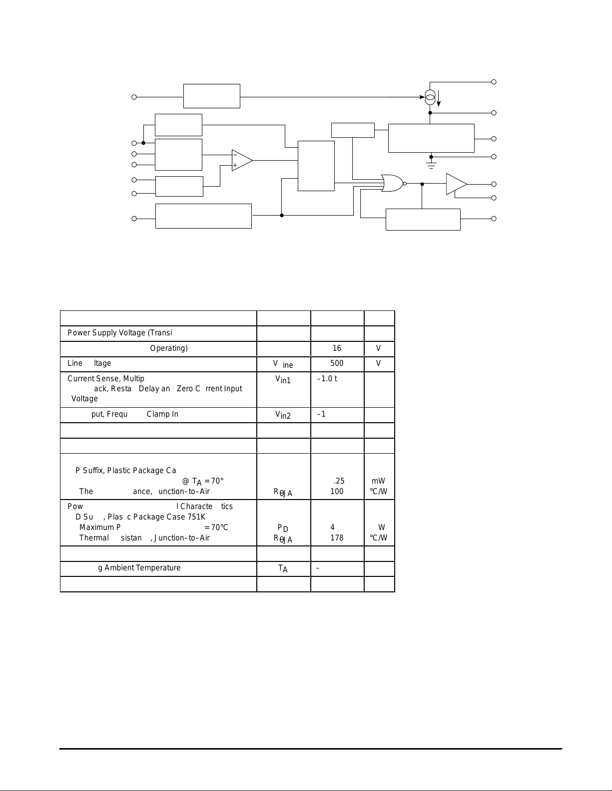
Representative Block Diagram
UVLO
PWM
This device contains 240 active transistors.
S
S
R
Q
Internal Bias
Generator
Frequency
Clamp
Line
V
CC
V
ref
AGnd
Gate
PGnd
Frequency
Clamp
MAXIMUM RATINGS (T
Power Supply Voltage (Transient)
Power Supply Voltage (Operating)
Line Voltage
Current Sense, Multiplier, Compensation, V oltage
Feedback, Restart Delay and Zero Current Input
Voltage
LEB Input, Frequency Clamp Input
Zero Current Detect Input
Restart Diode Current
Power Dissipation and Thermal Characteristics
P Suffix, Plastic Package Case 648
Maximum Power Dissipation @ TA = 70°C P
Thermal Resistance, Junction–to–Air R
Power Dissipation and Thermal Characteristics
D Suffix, Plastic Package Case 751K
Maximum Power Dissipation @ TA = 70°C P
Thermal Resistance, Junction–to–Air R
Operating Junction Temperature
Operating Ambient Temperature
Storage Temperature Range
NOTE: ESD data available upon request.
= 25°C, unless otherwise noted.)
A
Rating
Symbol Value Unit
V
V
V
V
V
T
CC
CC
Line
in1
in2
I
in
I
in
D
θJA
D
θJA
T
J
T
A
stg
20
16
500
–1.0 to +10 V
–1.0 to +20
±5.0
5.0
1.25 mW
100 °C/W
450 mW
178 °C/W
150
–25 to +125
–55 to +150
V
V
V
V
mA
mA
°C
°C
°C
2
MOTOROLA ANALOG IC DEVICE DATA
Page 3
MC33368
ÁÁÁ
ÁÁÁ
ÁÁÁ
Á
Á
Á
Á
Á
ÁÁÁ
Á
ÁÁÁ
ÁÁÁ
ÁÁÁ
ÁÁÁ
ÁÁÁ
Á
Á
Á
Á
Á
Á
Á
Á
Á
Á
Á
Á
ÁÁÁ
Á
Á
Á
ÁÁÁ
ÁÁÁ
ÁÁÁ
ÁÁÁ
ÁÁÁ
ÁÁÁ
Á
Á
Á
Á
Á
ÁÁÁ
Á
Á
Á
Á
Á
Á
ÁÁÁ
Á
Á
Á
Á
Á
Á
ÁÁÁ
Á
ÁÁÁ
ÁÁÁ
Á
Á
Á
Á
Á
ÁÁÁ
Á
Á
Á
Á
Á
Á
ÁÁÁ
Á
ÁÁÁ
ÁÁÁ
ÁÁÁ
ÁÁÁ
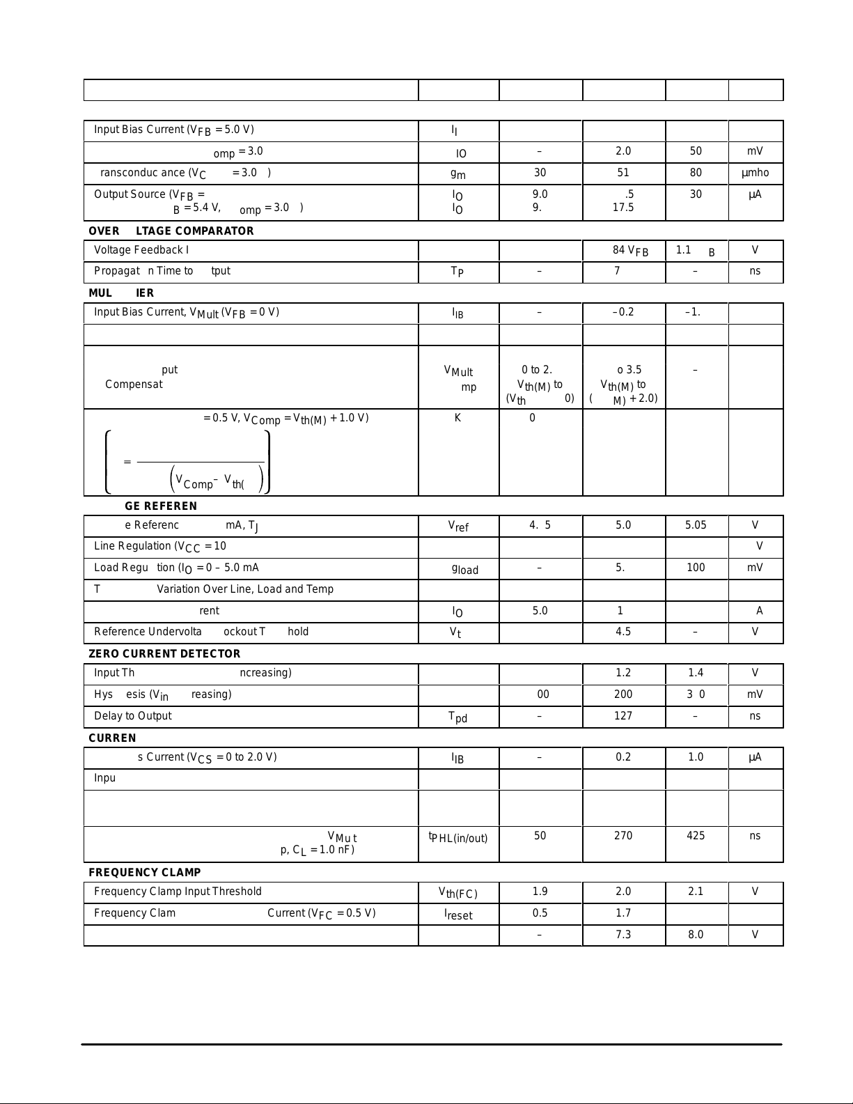
ELECTRICAL CHARACTERISTICS (V
= 14.5 V, for typical values TA = 25°C, for min/max values TJ = –25 to +125°C)
CC
Characteristic
ERROR AMPLIFIER
Input Bias Current (VFB = 5.0 V)
Input Offset Voltage (V
Transconductance (V
Output Source (VFB = 4.6 V, V
Output Sink (VFB = 5.4 V, V
БББББББББББББББ
Comp
Comp
= 3.0 V)
= 3.0 V)
Comp
Comp
= 3.0 V)
= 3.0 V)
OVERVOLTAGE COMPARATOR
Voltage Feedback Input Threshold
Propagation Time to Output
MULTIPLIER
Input Bias Current, V
Input Threshold, V
Mult
Comp
(VFB = 0 V)
Dynamic Input Voltage Range
Multiplier Input V
Compensation V
Multiplier Gain (V
ȡ
K
+
ȧ
V
Ȣ
Mult
= 0.5 V, V
Mult
VCSThreshold
ǒ
V
–V
Comp
th(M)
Comp
ȣ
ȧ
Ǔ
Ȥ
= V
+ 1.0 V) K 0.25 0.51 0.75 1/V
th(M)
VOLTAGE REFERENCE
Voltage Reference (IO = 0 mA, TJ = 25°C)
Line Regulation (VCC = 10 V to 16 V)
Load Regulation (IO = 0 – 5.0 mA)
Total Output Variation Over Line, Load and Temperature
Maximum Output Current
Reference Undervoltage Lockout Threshold
ZERO CURRENT DETECTOR
Input Threshold Voltage (Vin Increasing)
БББББББББББББББ
Hysteresis (Vin Decreasing)
БББББББББББББББ
Delay to Output
БББББББББББББББ
CURRENT SENSE COMPARATOR
Input Bias Current (VCS = 0 to 2.0 V)
Input Offset Voltage (V
Maximum Current Sense Input Threshold (V
БББББББББББББББ
V
= 5.0 V)
Mult
Delay to Output (V
БББББББББББББББ
(VCS = 0 to 5.0 V Step, CL = 1.0 nF)
LEB
= –0.2 V)
Mult
= 12 V, V
Comp
Comp
= 5.0 V, V
= 5.0 V,
= 5.0 V)
Mult
FREQUENCY CLAMP
Frequency Clamp Input Threshold
Frequency Clamp Capacitor Reset Current (VFC = 0.5 V)
Frequency Clamp Disable Voltage
Symbol Min Typ Max Unit
I
IB
V
IO
g
m
I
O
I
ÁÁÁ
O
V
FB(OV)
T
P
I
IB
V
th(M)
Mult
Comp
ÁÁÁ
ÁÁÁ
ÁÁÁ
V
ref
Reg
line
Reg
load
V
ref
I
O
V
th
V
th
ÁÁÁ
V
H
ÁÁÁ
T
pd
ÁÁÁ
I
IB
V
IO
V
th(max)
ÁÁÁ
t
PHL(in/out)
ÁÁÁ
V
th(FC)
I
reset
V
DFC
–
–
30
9.0
9.0
ÁÁÁ
1.07 V
FB
–
–
1.8
0
2.0
51
17.5
17.5
ÁÁÁ
1.084 V
FB
705
–0.2
2.1
0 to 2.5 0 to 3.5 –
V
to
th(M)
(V
+ 1.0)
th(M)
ÁÁÁ
ÁÁÁ
ÁÁÁ
4.95
–
–
4.8
5.0
–
1.0
ÁÁÁ
100
ÁÁÁ
–
ÁÁÁ
–
–
1.3
ÁÁÁ
50
ÁÁÁ
1.9
0.5
–
V
th(M)
(V
+ 2.0)
th(M)
ÁÁÁ
ÁÁÁ
ÁÁÁ
5.0
5.0
5.0
–
10
4.5
1.2
ÁÁÁ
200
ÁÁÁ
127
ÁÁÁ
0.2
4.0
1.5
ÁÁÁ
270
ÁÁÁ
2.0
1.7
7.3
to
1.0
50
80
30
30
ÁÁ
1.1 V
–
–1.0
2.4
–
ÁÁ
ÁÁ
ÁÁ
5.05
100
100
5.2
–
–
1.4
ÁÁ
300
ÁÁ
–
ÁÁ
1.0
50
1.8
ÁÁ
425
ÁÁ
2.1
4.0
8.0
ÁÁ
FB
ÁÁ
ÁÁ
ÁÁ
ÁÁ
ÁÁ
ÁÁ
ÁÁ
ÁÁ
µA
mV
µmho
µA
V
ns
µA
V
V
V
mV
mV
V
mA
V
V
mV
ns
µA
mV
V
ns
V
mA
V
MOTOROLA ANALOG IC DEVICE DATA
3
Page 4
MC33368
ÁÁÁ
Á
Á
Á
Á
Á
ÁÁÁ
Á
ÁÁÁ
ÁÁÁ
ÁÁÁ
ÁÁÁ
ÁÁÁ
ÁÁÁ
ÁÁÁ
ÁÁÁ
ÁÁÁ
ÁÁÁ
ÁÁÁ
ÁÁÁ
ÁÁÁ
ÁÁÁ
ÁÁÁ
ÁÁÁ
Á
Á
Á
Á
Á
ÁÁÁ
Á
Á
Á
Á
Á
Á
ÁÁÁ
Á
ÁÁÁ
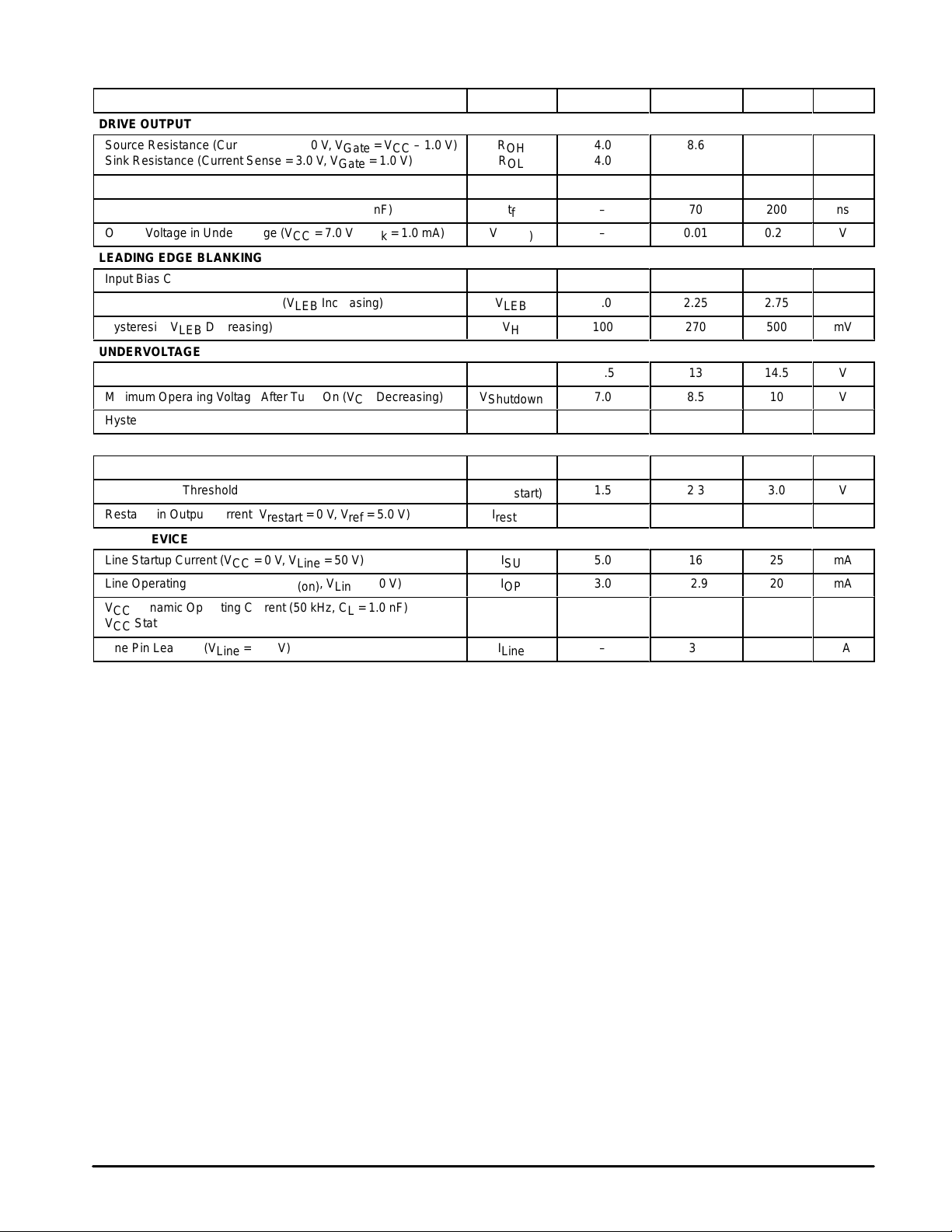
ELECTRICAL CHARACTERISTICS
(continued) (VCC = 14.5 V, for typical values TA = 25°C, for min/max values TJ = –25 to +125°C)
Characteristic UnitMaxTypMinSymbol
DRIVE OUTPUT
Source Resistance (Current Sense = 0 V, V
Sink Resistance (Current Sense = 3.0 V, V
БББББББББББББББ
= VCC – 1.0 V)
Gate
= 1.0 V)
Gate
Output Voltage Rise T ime (25% – 75%) (CL = 1.0 nF)
Output Voltage Fall Time (75% – 25%) (CL = 1.0 nF)
Output Voltage in Undervoltage (VCC = 7.0 V, I
Sink
= 1.0 mA)
LEADING EDGE BLANKING
Input Bias Current
Threshold (as Offset from VCC) (V
Hysteresis (V
Decreasing)
LEB
Increasing)
LEB
UNDERVOLTAGE LOCKOUT
Startup Threshold (VCC Increasing)
Minimum Operating Voltage After Turn–On (VCC Decreasing)
Hysteresis
TIMER
Watchdog Timer
Restart Timer Threshold
Restart Pin Output Current (V
restart
= 0 V, V
= 5.0 V)
ref
TOTAL DEVICE
Line Startup Current (VCC = 0 V, V
БББББББББББББББ
Line Operating Current (VCC = V
VCC Dynamic Operating Current (50 kHz, CL = 1.0 nF)
БББББББББББББББ
VCC Static Operating Current (IO = 0)
Line Pin Leakage (V
Line
= 500 V)
Line
th(on)
= 50 V)
, V
= 50 V) I
Line
R
OH
R
ÁÁÁ
OL
t
r
t
f
V
O(UV)
I
bias
V
LEB
V
H
V
th(on)
V
Shutdown
V
H
t
DLY
V
th(restart)
I
restart
I
SU
ÁÁÁ
OP
I
CC
ÁÁÁ
I
Line
4.0
4.0
ÁÁÁ
–
–
–
–
1.0
100
11.5
7.0
–
180
1.5
3.1
5.0
ÁÁÁ
8.6
7.2
ÁÁÁ
55
70
0.01
0.1
2.25
270
13
8.5
4.5
385
2.3
5.2
16
ÁÁÁ
20
20
ÁÁ
200
200
0.25
0.5
2.75
500
14.5
10
–
800
3.0
7.1
25
ÁÁ
3.0 12.9 20 mA
–
ÁÁÁ
–
–
5.3
ÁÁÁ
3.0
30
8.5
ÁÁ
–
80
Ω
ÁÁ
ns
ns
V
µA
V
mV
V
V
V
µs
V
mA
mA
ÁÁ
mA
ÁÁ
µA
4
MOTOROLA ANALOG IC DEVICE DATA
Page 5
MC33368
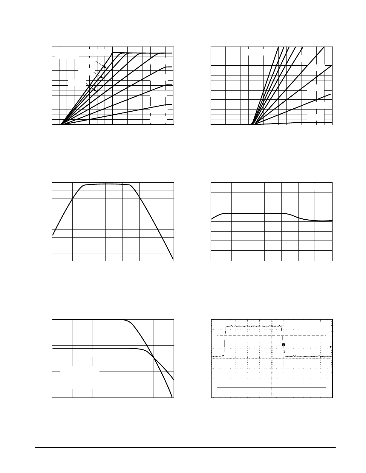
Figure 1. Current Sense Input Threshold
versus Multiplier Input
1.6
, CURRENT SENSE PIN 6 THRESHOLD (V)
V
CS
1.4
1.2
1.0
0.8
0.6
0.4
0.2
0
–0.2
VCC = 14 V
TA = 25
V
= 4.0 V
Pin 4
°
C
= 3.75 V
= 3.5 V
= 3.25 V
0.6 1.4 2.2 3.0 –0.06 0 0.06 0.12 0.20
VM, MULTIPLIER PIN 5 INPUT VOLTAGE (V)
Figure 3. Reference V oltage versus Temperature
16
12
= 3.0 V
= 2.75 V
= 2.5 V
= 2.25 V
= 2.0 V
VCC = 14 V
, CURRENT SENSE PIN 6 THRESHOLD (V)
0.08
0.07
0.06
0.05
0.04
0.03
0.02
0.01
CS
FB
Figure 2. Current Sense Input Threshold
versus Multiplier Input, Expanded View
V
= 4.0 V
Pin 4
0
–0.12
VM, MULTIPLIER PIN 5 INPUT VOLTAGE (V)
Figure 4. Overvoltage Comparator Input
Threshold versus T emperature
110
109
= 3.0 V
= 2.75 V
= 2.5 V
= 2.25 V
= 2.0 V
VCC = 14 V
8.0
4.0
CHANGE (mV)
0
, VOLTAGE FEEDBACK THRESHOLD
FB
V
∆
–4.0
–55
–25 0 25 50 75 125100 –25 0 25 50 75 100 125
TA, AMBIENT TEMPERATURE (°C)
Figure 5. Error Amplifier Transconductance
and Phase versus Frequency
100
80
µ
60
40
20
, TRANSCONDUCTANCE ( mho)
0
m
g
–20
10
Transconductance
VCC = 14 V
VO = 2.0 to 4.0 V
Ω
RL = 10 k
TA = 25°C
100 1.0 k 10 k 100 k 1.0 M 10 M
f, FREQUENCY (Hz)
Phase
108
107
, OVERVOL TAGE INPUT THRESHOLD (% V ) V
106
–55
FB(OV)
V
Figure 6. Error Amplifier Transient Response
0
30
60
90
120
150
180
6.0 V
4.0 V
2.0 V
0 V
, EXCESS PHASE (DEGREES)
θ
–1.0 V
TA, AMBIENT TEMPERATURE (
5.0 µs/DIV
°
C)
VCC = 14 V
TA = 25
°
C
MOTOROLA ANALOG IC DEVICE DATA
5
Page 6

MC33368
1.80
1.76
1.72
1.68
, QUICKSTAR T CHARGE VOLTAGE (V)
chg
V
1.64
–55
20
15
10
Figure 7. Quickstart Charge Current
versus T emperature
VCC = 14 V
Voltage
Current
–25 0 25 50 75 100 125 –25 0 25 50 75 100 125
TA, AMBIENT TEMPERATURE (°C)
1.50
1.30
1.10
0.90
0.70
µ
, WATCHDOG TIME DELAY ( s)
t
, QUICKSTAR T CHARGE CURRENT (mA)
chg
I
500
460
420
380
DLY
340
–55
Figure 8. Watchdog Timer Delay
versus T emperature
VCC = 14 V
TA, AMBIENT TEMPERATURE (°C)
Figure 10. Supply Current versus
Figure 9. Drive Output Waveform
VCC = 14 V
CL = 1000 pF
TA = 25
6.0
Pulse tested with a 4.0 V peak, 50 kHz square
°
C
wave through a 22 k resistance into Pin 7.
4.0
Supply V oltage
5.0
OUTPUT VOLTAGE (V)
–5.0
1000
°
100
, THERMAL RESISTANCE
JA(t)
JUNCTION–TO–AIR ( C/W)
θ
R
0
5.0 µs/DIV
Figure 11. Transient Thermal Resistance
10
0.01
0.1 1.0 10 100
t, TIME (s)
CO = 1000 pF
Pin 3, 6, 8= Gnd
2.0
, SUPPLY CURRENT (mA)
Pin 5 = 1.0 k to Gnd
CC
TA = 25
I
0
2.0
400
200
0
OUTPUT VOLTAGE (V)
°
C
4.0 6.0 8.0 10 12 14
VCC, SUPPLY VOLTAGE (V)
Figure 12. Low Load Detection
Response Waveform
Output
Voltage
Load
Current
200 ms/DIV
3.0
2.0
1.0
OUTPUT CURRENT (A)
0
6
MOTOROLA ANALOG IC DEVICE DATA
Page 7

MC33368
FUNCTIONAL DESCRIPTION
INTRODUCTION
With the goal of exceeding the requirements of legislation
on line current harmonic content, there is an ever increasing
demand for an economical method of obtaining a unity power
factor. This data sheet describes a monolithic control IC that
was specifically designed for power factor control with
minimal external components. It offers the designer a simple
cost effective solution to obtain the benefits of active power
factor correction.
Most electronic ballasts and switching power supplies use
a bridge rectifier and a bulk storage capacitor to derive raw dc
voltage from the utility ac line, Figure 13.
Figure 13. Uncorrected Power Factor Circuit
Converter
Load
AC
Line
Rectifiers
Bulk
Storage
Capacitor
This simple rectifying circuit draws power from the line
when the instantaneous ac voltage exceeds the capacitor
voltage. This occurs near the line voltage peak and results in
a high charge current spike, Figure 14. Since power is only
taken near the line voltage peaks, the resulting spikes of
current are extremely nonsinusoidal with a high content of
harmonics. This results in a poor power factor condition
where the apparent input power is much higher than the real
power. Power factor ratios of 0.5 to 0.7 are common.
Figure 14. Uncorrected Power Factor Input Waveforms
V
pk
Rectified
DC
0
AC Line
Voltage
0
AC Line
Current
Line Sag
Power factor correction can be achieved with the use of
either a passive or active input circuit. Passive circuits
usually contain a combination of large capacitors, inductors,
and rectifiers that operate at the ac line frequency. Active
circuits incorporate some form of a high frequency switching
converter for the power processing with the boost converter
being the most popular topology. Since active input circuits
operate at a frequency much higher than that of the ac line,
they are smaller, lighter in weight, and more efficient than a
passive circuit that yields similar results. With proper control
of the preconverter, almost any complex load can be made to
appear resistive to the ac line, thus significantly reducing the
harmonic current content.
Operating Description
The MC33368 contains many of the building blocks and
protection features that are employed in modern high
performance current mode power supply controllers.
Referring to the block diagram in Figure 15, note that a
multiplier has been added to the current sense loop and that
this device does not contain an oscillator. A description of
each of the functional blocks is given below.
Error Amplifier
An Error Amplifier with access to the inverting input and
output is provided. The amplifier is a transconductance type,
meaning that it has high output impedance with controlled
voltage–to–current gain (gm 50 µmhos). The noninverting
input is internally biased at 5.0 V ±2.0%. The output voltage
of the power factor converter is typically divided down and
monitored by the inverting input. The maximum input bias
current is –1.0 µA which can cause an output voltage error
that is equal to the product of the input bias current and the
value of the upper divider resistor R2. The Error Amplifier
output is internally connected to the Multiplier and is pinned
out (Pin 4) for external loop compensation. Typically, the
bandwidth is set below 20 Hz so that the amplifier’s output
voltage is relatively constant over a given ac line cycle. In
effect, the error amplifier monitors the average output voltage
of the converter over several line cycles resulting in a fixed
Drive Output on–time. The amplifier output stage can sink
and source 11.5 µA of current and is capable of swinging
from 1.7 to 5.0 V, assuring that the Multiplier can be driven
over its entire dynamic range.
Note that by using a transconductance type amplifier, the
input is allowed to move independently with respect to the
output, since the compensation capacitor is connected to
ground. This allows dual usage of the Voltage Feedback pin
by the Error Amplifier and Overvoltage Comparator.
Overvoltage Comparator
An Overvoltage Comparator is incorporated to eliminate
the possibility of runaway output voltage. This condition can
occur during initial startup, sudden load removal, or during
output arcing and is the result of the low bandwidth that must
be used in the Error Amplifier control loop. The Overvoltage
Comparator monitors the peak output voltage of the
converter, and when exceeded, immediately terminates
MOSFET switching. The comparator threshold is internally
set to 1.08 V
. In order to prevent false tripping during
ref
normal operation, the value of the output filter capacitor C3
must be large enough to keep the peak–to–peak ripple less
than 16% of the average dc output.
MOTOROLA ANALOG IC DEVICE DATA
7
Page 8

MC33368
Multiplier
A single quadrant, two input multiplier is the critical
element that enables this device to control power factor. The
ac haversines are monitored at Pin 5 with respect to ground
while the Error Amplifier output at Pin 4 is monitored with
respect to the Voltage Feedback Input threshold. A graph of
the Multiplier transfer curve is shown in Figure 1. Note that
both inputs are extremely linear over a wide dynamic range,
0 to 3.2 V for Pin 5 and 2.5 to 4.0 V for Pin 4. The Multiplier
output controls the Current Sense Comparator threshold as
the ac voltage traverses sinusoidally from zero to peak line.
This has the effect of forcing the MOSFET on–time to track
the input line voltage, thus making the preconverter load
appear to be resistive.
Pin 6 Threshold[0.55
Zero Current Detector
The MC33368 operates as a critical conduction current
mode controller, whereby output switch conduction is
initiated by the Zero Current Detector and terminated when
the peak inductor current reaches the threshold level
established by the Multiplier output. The Zero Current
Detector initiates the next on–time by setting the RS Latch at
the instant the inductor current reaches zero. This critical
conduction mode of operation has two significant benefits.
First, since the MOSFET cannot turn–on until the inductor
current reaches zero, the output rectifier’s reverse recovery
time becomes less critical allowing the use of an inexpensive
rectifier. Second, since there are no deadtime gaps between
cycles, the ac line current is continuous thus limiting the peak
switch to twice the average input current
The Zero Current Detector indirectly senses the inductor
current by monitoring when the auxiliary winding voltage falls
below 1.2 V . To prevent false tripping, 200 mV of hysteresis is
provided. The Zero Current Detector input is internally
protected by two clamps. The upper 10 V clamp prevents
input overvoltage breakdown while the lower –0.7 V clamp
prevents substrate injection. An external resistor must be
used in series with the auxiliary winding to limit the current
through the clamps to 5.0 mA or less.
Current Sense Comparator and RS Latch
The Current Sense Comparator RS Latch configuration
used ensures that only a single pulse appears at the Drive
Output during a given cycle. The inductor current is
converted to a voltage by inserting a ground–referenced
sense resistor R7 in series with the source of output switch.
This voltage is monitored by the Current Sense Input and
compared to a level derived from the Multiplier output. The
peak inductor current under normal operating conditions is
controlled by the threshold voltage of Pin 6 where:
Ipk+
Abnormal operating conditions occur when the
preconverter is running at extremely low line or if output
voltage sensing is lost. Under these conditions, the Current
Sense Comparator threshold will be internally clamped to
1.5 V. Therefore, the maximum peak switch current is:
I
pk(max)
ǒ
V
Pin 4–VPin 3
Pin 6 Threshold
R7
1.5 V
+
R7
Ǔ
V
Pin 5
With the component values shown in Figure 15, the
Current Sense Comparator threshold, at the peak of the
haversine, varies from 110 mV at 90 Vac to 100 mV at
268 Vac. The Current Sense Input to Drive Output
propagation delay is typically 200 ns.
Timer
A watchdog timer function was added to the IC to
eliminate the need for an external oscillator when used in
stand alone applications. The Timer provides a means to
automatically start or restart the preconverter if the Drive
Output has been off for more than 385 µs after the inductor
current reaches zero.
Undervoltage Lockout and Quickstart
The MC33368 has a 5.0 V internal reference brought out
to Pin 1 and capable of sourcing 10 mA typically. It also
contains an Undervoltage Lockout (UVLO) circuit which
suppresses the Gate output at Pin 11 if the VCC supply
voltage drops below 8.5 V typical.
A Quickstart circuit has been incorporated to optimize
converter startup. During initial startup, compensation
capacitor C1 will be discharged, holding the Error Amplifier
output below the Multiplier’s threshold. This will prevent Drive
Output switching and delay bootstraping of capacitor C4 by
diode D6. If Pin 4 does not reach the multiplier threshold
before C4 discharges below the lower SMPS UVLO
threshold, the converter will hiccup and experience a
significant startup delay . The Quickstart circuit is designed to
precharge C1 to 1.7 V. This level is slightly below the Pin 4
Multiplier threshold, allowing immediate Drive Output
switching.
Restart Delay
A restart delay pin is provided to allow hiccup mode fault
protection in case of a short circuit condition and to prevent
the SMPS from repeatedly trying to restart after the input line
voltage has been removed. When power is first applied, there
is no startup delay , but subsequent cycling of the VCC voltage
will result in delay times that are programmed by an external
resistor and capacitor. The Restart Delay, Pin 2, is a high
impedance, so that an external capacitor can provide delay
times as long as several seconds.
If the SMPS output is short circuited, the transformer
winding, which provides the VCC voltage to the control IC and
the MC33368, will be unable to sustain VCC to the control
circuits. The restart delay capacitor at Pin 2 of the MC33368
prevents the high voltage startup transistor within the IC from
maintaining the voltage on C4. After VCC drops below the
UVLO threshold in the SMPS, the SMPS switching
transistors are held off for the time programmed by the values
of the restart capacitor (C9) and resistor (R8). In this manner,
the SMPS switching transistors are operated at very low duty
cyles, preventing their destruction. If the short circuit fault is
removed, the power supply system will turn on by itself in a
normal startup mode after the restart delay has timed out.
8
MOTOROLA ANALOG IC DEVICE DATA
Page 9

MC33368
Output Switching Frequency Clamp
In normal operation, the MC33368 operates the boost
inductor in the critical mode. That is, the inductor current
ramps to a peak value, ramps down to zero, then immediately
begins ramping positive again. The peak current is
programmed by the multiplier output within the IC. As the
input voltage haversine declines to near zero, the output
switch on–time becomes constant, rather than going to zero
because of the small integrated dc voltage at Pin 5 caused by
C2, R3 and R5. Because of this, the average line current
does not exactly follow the line voltage near the zero
crossings. The Output Switching Frequency Clamp remedies
this situation to improve power factor and minimize EMI
generated in this operating region. The values of R10 and
C7, as shown in Figure 15, program a minimum off–time in
the frequency clamp which overrides the zero current detect
signal, forcing a minimum off–time. This allows discontinuous
conduction operation of the boost inductor in the zero
crossing region, and the average line current more nearly
follows the voltage. The Output Switching Frequency Clamp
function can be disabled by connecting the FC input, Pin 13,
to the VCC supply Pin 12.
For best results, the minimum off–time, determined by
the values of R10 and C7, should be chosen so that
t
= t
s(min)
voltage at the frequency clamp input is less than 2.0 V . When
the output drive is high, C7 is discharged through an internal
100 µA current source. When the output drive switches low,
C7 is charged through R10. The drive output is inhibited until
the voltage across C7 reaches 2.0 V, establishing a minimim
off–time where:
t
Output
The IC contains a CMOS output driver that was
specifically designed for direct drive of power MOSFET s. The
Gate Output is capable of up to ±1500 mA peak current with
a typical rise and fall time of 50 ns with a 1.0 nF load.
Additional internal circuitry has been added to keep the Gate
Output in a sinking mode whenever the Undervoltage
Lockout is active. This characteristic eliminates the need for
an external gate pull–down resistor. The totem–pole output
has been optimized to minimize cross–conduction current
during high speed operation.
(on)
(off)fc
+ t
(off)fc
+*
. Output drive is inhibited when the
R10 C7 log
1
ƪ
e
*
2
ǒ
Ǔ
ƫ
V
CC
MOTOROLA ANALOG IC DEVICE DATA
9
Page 10

MC33368
T able 1. Design Equations
Calculation Formula Notes
Converter Output Power
Peak Indicator Current
Inductance
LP+
Switch On–Time
Switch Off–Time
Minimum Switch
Off–Time
Delay Time
Switching Frequency
Peak Switch Current
Multiplier Input Voltage
Converter Output
Voltage
Converter Output
Peak–to–Peak
Ripple Voltage
Error Amplifier
Bandwidth
NOTE:The following converter characteristics must be chosen:
VO = Desired output voltage. Vac
IO = Desired output current. ∆VO = Converter output peak–to–peak ripple voltage.
Vac = AC RMS operating line voltage.
D
V
O(pp)
t
td+
VO+
PO+
I
L(pk)
V
O
ǒ
t
Ǹ
2
t
(on)
+
(off)
Ǹ
t
(off)
min
–R10C7ln
f
+
VM+
V
ref
+
I
L(pk)
BW
VOI
O
Ǹ
P
22
O
h
Vac
(LL)
Vac
–1
Ǔ
(LL)
Ǔ
2
)
2
ESR
Ǔ
h
(LL)
2
VOP
O
2POL
P
2
h
Vac
t
(on)
O
Ť
q
LPI
L(pk)
V
O
VCC–2
ǒ
V
CC
1
)
t
(off)
V
CS
I
L(pk)
Ǹ
Vac 2
R5
Ǔ
)
1
R3
Ǔ
–IIBR1
)
1
1
2pfacC3
g
m
2pC1
= AC RMS minimum required operating line voltage for output regulation.
–Vac
+
2
t
R7
Ǹ
+
Ǹ
V
VacŤSin
+
(on)
+
ǒ
R2
ǒ
R1
ǒ
+
(LL)
Calculate the maximum required output power.
Calculated at the minimum required ac line voltage for
output regulation. Let the efficiency η = 0.92 for low line
operation.
Let the switching cycle t = 40 µs for universal input (85 to
265 Vac) operation and 20 µs for fixed input (92 to
138 Vac, or 184 to 276 Vac) operation.
In theory, the on–time t
tends to increase at the ac line zero crossings due to the
charge on capacitor C5. Let Vac = Vac
and t
The off–time t
voltage and approaches zero at the ac line zero crossings.
Theta (θ) represents the angle of the ac line voltage.
The off–time is at a minimum at ac line crossings. This
equation is used to calculate t
zero.
The delay time is used to override the minimum off–time at
the ac line zero crossings by programming the Frequency
Clamp with C7 and R10.
The minimum switching frequency occurs at the peak of
the ac line voltage. As the ac line voltage traverses from
peak to zero, t
in switching frequency.
Set the current sense threshold VCS to 1.0 V for universal
input (85 to 265 Vac) operation and to 0.5 V for fixed input
(92 to 138 Vac, or 184 to 276 Vac) operation. Note that V
must be less than 1.4 V.
Set the mulltiplier input voltage VM to 3.0 V at high line.
Empirically adjust VM for the lowest distortion over the ac
line voltage range while guaranteeing startup at minimum
line.
The IIB R1 error term can be minimized with a divider
current in excess of 100 µA.
The calculated peak–to–peak ripple must be less than 16%
of the average dc output voltage to prevent false tripping of
2
the Overvoltage Comparator. Refer to the Overvoltage
Comparator Text. ESR is the equivalent series resistance
of C3.
The bandwidth is typically set to 20 Hz. When operating at
high ac line, the value of C1 may need to be increased.
calculations.
(off)
(off)
(off)
is constant. In practice, t
(on)
for initial t
(LL)
is greatest at the peak of the ac line
as Theta approaches
(off)
approaches zero producing an increase
(on)
(on)
CS
10
MOTOROLA ANALOG IC DEVICE DATA
Page 11

MC33368
Figure 15. 80 W Power Factor Controller
92 to
270 Vrms
330
R5
1.3 M
R3
20 k
R8
10 k
C9
µ
1N4006
D2 D4
V
F
EMI
Filter
ref
D1 D3
V
ref
RD
2
AGnd
8
1.5 V
Load Detect
Mult
5
Multiplier
C2
0.01
T: Coilcraft N2881–A
Primary = 62 turns of #22 AWG
Secondary = 5 turns of #22 AWG
Core = Coilcraft PT2510, EE25
Gap = 0.072
″
total for a primary inductance (Lp) of 320
C5
1.0
MC33368
15 V
Q
Timer R
RS Latch
R
R
S
S
Q
S
Set Dominant
Overvoltage
Comparator
Low
1.08 x V
ref
Quickstart
Reference
Comp FB
C1
0.68
V
ref
C6
0.1
Zero
Current
Detect
Leading Edge
5.0 V
V
µ
H
UVLO
1.2/1.0
Frequency
Clamp
Blanking
ref
16
Line
V
CC
12
13/8.0
7
ZCD
Gate
11
PGnd
10
13
FC
9
LEB
6
CS
314
Not Used: D7, C8, R6, R9
1N4744
15 V
D8
R4
22 k
To V
Pin 12
R13
C4
100
51
R11
10
CC
R10
10
C7
10 pF
D6
1N4934
Q1
T
320
µ
H
MUR130
D5
C3
220
MTP8N50E
R7
0.1
0.25 W
V
O
R2
470 k
R1
10 k
AC Line Input
V
Pin PF I
rms
90 79.7 0.999 0.89 0.5 0.15 0.09 0.06 0.09 3.0 244.4 0.31 76.01 95.4
100 79.3 0.998 0.79 0.5 0.14 0.09 0.08 0.10 3.0 242.9 0.31 75.54 95.3
110 78.9 0.997 0.72 0.5 0.16 0.13 0.08 0.10 3.0 242.9 0.31 75.30 95.4
120 78.5 0.996 0.66 0.5 0.15 0.12 0.08 0.13 3.0 243.0 0.31 75.57 96.3
130 78.1 0.994 0.60 0.5 0.14 0.12 0.07 0.14 3.0 243.0 0.31 75.57 96.7
138 77.8 0.991 0.57 0.5 0.15 0.14 0.08 0.14 3.0 243.0 0.31 75.57 97.1
Heatsink = AAVID Engineering Inc., 590302B03600, or 593002B03400
fund
MOTOROLA ANALOG IC DEVICE DATA
Power Factor Controller Test Data
Current Harmonic Distortion (% I
THD2357V
)
fund
O(pp)VOIOPO
DC Output
n(%)
11
Page 12

MC33368
Figure 16. 175 W Universal Input Power Factor Controller
92 to
270 Vrms
1.0 M
R5
1.3 M
R3
10 k
R8
C9
2.2
EMI
Filter
V
ref
D2 D4
RD
2
AGnd
8
Mult
5
C2
0.01
1N5406
D1 D3
V
ref
1.5 V
Multiplier
C5
1.0
MC33368
15 V
Timer R
Q
RS Latch
R
R
S
S
Q
S
Set Dominant
Overvoltage
Comparator
Low
Load Detect
Not Used: D7, C7, C8, R6, R9, R10
1.08 x V
ref
Quickstart
Reference
Comp FB
C1
2.2
V
ref
C6
0.1
Zero
Current
Detect
Leading Edge
5.0 V
V
ref
UVLO
Frequency
Clamp
Blanking
16
1.2/1.0
Line
13/8.0
314
6.9 V
R13
D8
V
1N4744
CC
12
7
15 V
ZCD
Gate
11
PGnd
10
13
FC
LEB
CS
R4
22 k
To V
Pin 12
9
6
T: Coilcraft N2880–A
L = 870 µHy
Primary: 78 turns of #16 AWG
Secondary: 6 turns of #18 AWG
Core: Coilcraft PT4215, EE42–15
Gap: 0.104
″
51
C4
100
CC
total
R11
10
D6
1N4934
Q1
T
MUR460
D5
MTW20N50E
R7
0.1
C3
330
V
O
R2
820 k
R1
10 k
12
Power Factor Controller Test Data
AC Line Input
Current Harmonic Distortion (% I
V
Pin PF I
rms
90 190.4 0.995 2.11 5.8 0.16 0.32 0.24 0.80 3.6 398.0 0.44 175.9 92.4
120 192.1 0.997 1.60 3.2 0.08 0.17 0.07 0.30 3.6 398.9 0.44 177.1 92.2
138 192.7 0.997 1.40 0.9 0.08 0.24 0.03 0.15 3.6 402.3 0.45 179.0 92.9
180 194.3 0.995 1.08 0.9 0.04 0.18 0.04 0.08 3.6 409.1 0.45 182.9 94.1
240 189.3 0.983 0.80 0.7 0.08 0.21 0.08 0.06 3.6 407.0 0.45 181.1 95.7
268 186.3 0.972 0.71 0.6 0.11 0.32 0.10 0.10 3.6 406.2 0.44 180.4 96.8
Heatsink = AAVID Engineering Inc., 590302B03600
THD2357V
fund
)
fund
O(pp)VOIOPO
DC Output
MOTOROLA ANALOG IC DEVICE DATA
n(%)
Page 13

MC33368
Figure 17. Power Factor Test Setup
2X Step–up
Isolation
Autoformer
Line
115 Vrms
Input
Neutral
An RFI filter is required for best performance when connecting the preconverter directly to the ac line. The filter attenuates the level of high
frequency switching that appears on the ac line current waveform. Figures 15 and 16 work well with commercially available two stage filters such
as the Delta Electronics 03DPCG6. Shown above is a single stage test filter that can easily be constructed with four ac line rated capacitors and
a common–mode transformer. Coilcraft CMT3–28–2 was used to test Figures 15 and 16. It has a minimum inductance of 28 mH and a maximum
current rating of 2.0 A. Coilcraft CMT4–17–9 was used to test Figure 19. It has a minimum inductance of 17 mH and a maximum current rating of
9.0 A. Circuit conversion efficiency η (%) was calculated without the power loss of the RFI filter.
Transformer
AC Power
Analyzer
PM 1000
10
WVAPFV
VDAcf Ainst Freq HARM
HI HI
rmsArms
A V
L.O. L.O.
Voltech
Figure 18. On/Off Control
EMI Filter
T
0.1 1.0
0 to 270 Vac
Output to
Power Factor
Correction
Circuit
270 Vrms
1N4148
On/Off
Input
5.0 V Off
0 V On
92 to
10 k
330
R5
1.3 M
R3
10 k
EMI
Filter
R8
C9
µ
F
V
ref
AGnd
C2
0.01
D2 D4
D1 D3
V
ref
RD
2
8
1.5 V
Mult
5
Multiplier
C5
1.0
MC33368
15 V
Timer R
Q
RS Latch
R
R
S
S
Q
S
Set Dominant
Overvoltage
Comparator
Low
Load Detect
1.08 x V
ref
Quickstart
Reference
Comp FB
C1
22
1.0 k
V
ref
C6
0.1
1.0 k
Zero
Current
Detect
Leading Edge
5.0 V
V
ref
UVLO
Frequency
Clamp
Blanking
2N3904
V
CC
16
1.2/1.0
10 k
Line
13/8.0
314
6.9 V
V
CC
12
7
ZCD
Gate
11
PGnd
10
13
FC
9
LEB
6
CS
D8
15 V
R4
22 k
R13
C4
100
51
R11
10
D6
T
Q1
D5
C3
330
MTW14N50E
R2
820 k
R7
0.1
R1
10 k
DC
Out
MOTOROLA ANALOG IC DEVICE DATA
13
Page 14

MC33368
Figure 19. 400 W Power Factor Controller
92 to
270 Vac
R5
1.3 M
R3
10.5 k
1.0 M
330
EMI
Filter
V
R8
C9
µ
F
D2 D4
D1 D3
ref
RD
AGnd
Mult
C2
0.01
2
8
5
1N5406
V
ref
1.5 V
Multiplier
C5
1.0
MC33368
15 V
Timer R
Q
RS Latch
R
R
S
S
Q
S
Set Dominant
Overvoltage
Comparator
Low
Load Detect
1.08 x V
ref
Quickstart
Reference
Comp FB
C1
1.0
V
ref
C6
0.1
Zero
Current
Detect
Leading Edge
5.0 V
V
ref
UVLO
Frequency
Clamp
Blanking
16
1.2/1.0
Line
13/8.0
314
1.5 V
1N4744
V
CC
12
7
ZCD
Gate
11
PGnd
10
13
FC
9
LEB
6
CS
D8
15 V
C4
100
R4
22 k
V
ref
C8
0.001
R13
51
R11
10
R10
10 k
C7
470 pF
R9
10
D6
1N4934
T
Q1
MUR460
D5
C3
330
MTW20N50E
R2
820 k
R7
0.1
R1
10 k
400 V
14
MOTOROLA ANALOG IC DEVICE DATA
Page 15

MC33368
Figure 20. Printed Circuit Board and Component Layout
(Circuits of Figures 15 and 16)
DC Output
R2
C9
C7
R10
J = Jumper
D7
R1
D3
C6
R3
C2
R5
C1
R8
J
IC1
R4
R11
C8
J
R13
J
R9
C3
R6
D6
D1
D2 D4
R7
J
Q1
DGS
D5
(Top View)
4.5
AC Input
C5
C4
Transformer
D8
″
3.0
MC33368
″
(Bottom View)
MOTOROLA ANALOG IC DEVICE DATA
15
Page 16

–A–
916
B
18
F
C
S
–T–
H
G
D
16 PL
0.25 (0.010) T
K
M
-A-
16
9
SM
B
-B-
P
0.25 (0.010)
18
G
C
-T-
K
D 14 PL
0.25 (0.010)
T
AB
SM S
MC33368
OUTLINE DIMENSIONS
P SUFFIX
PLASTIC PACKAGE
CASE 648–08
(DIP–16)
ISSUE R
L
SEATING
PLANE
J
M
A
D SUFFIX
PLASTIC PACKAGE
CASE 751K–01
(SO–16)
ISSUE O
_
R X 45
SEATING
PLANE
J
NOTES:
1. DIMENSIONING AND TOLERANCING PER ANSI
Y14.5M, 1982.
2. CONTROLLING DIMENSION: INCH.
3. DIMENSION L TO CENTER OF LEADS WHEN
FORMED PARALLEL.
4. DIMENSION B DOES NOT INCLUDE MOLD FLASH.
5. ROUNDED CORNERS OPTIONAL.
DIM MIN MAX MIN MAX
A 0.740 0.770 18.80 19.55
B 0.250 0.270 6.35 6.85
C 0.145 0.175 3.69 4.44
D 0.015 0.021 0.39 0.53
F 0.040 0.70 1.02 1.77
M
_
M
F
G 0.100 BSC 2.54 BSC
H 0.050 BSC 1.27 BSC
J 0.008 0.015 0.21 0.38
K 0.110 0.130 2.80 3.30
L 0.295 0.305 7.50 7.74
M 0 10 0 10
S 0.020 0.040 0.51 1.01
NOTES:
1 DIMENSIONING AND TOLERANCING PER ANSI
Y14.5M, 1982.
2 CONTROLLING DIMENSION: MILLIMETER.
3 DIMENSIONS A AND B DO NOT INCLUDE MOLD
PROTRUSION.
4 MAXIMUM MOLD PROTRUSION 0.15 (0.006) PER
SIDE.
5 DIMENSION D DOES NOT INCLUDE DAMBAR
PROTRUSION. ALLOWABLE DAMBAR
PROTRUSION SHALL BE 0.127 (0.005) TOTAL IN
EXCESS OF THE D DIMENSION AT MAXIMUM
MATERIAL CONDITION.
DIMAMIN MAX MIN MAX
B 3.80 4.00 0.150 0.157
C 1.35 1.75 0.054 0.068
D 0.35 0.49 0.014 0.019
F 0.40 1.25 0.016 0.049
G 1.27 BSC 0.050 BSC
J 0.19 0.25 0.008 0.009
K 0.10 0.25 0.004 0.009
M 0 7 0 7
P 5.80 6.20 0.229 0.244
R 0.25 0.50 0.010 0.019
MILLIMETERSINCHES
____
MILLIMETERS
9.80 10.00 0.368 0.393
____
INCHES
Motorola reserves the right to make changes without further notice to any products herein. Motorola makes no warranty , representation or guarantee regarding
the suitability of its products for any particular purpose, nor does Motorola assume any liability arising out of the application or use of any product or circuit, and
specifically disclaims any and all liability, including without limitation consequential or incidental damages. “T ypical” parameters which may be provided in Motorola
data sheets and/or specifications can and do vary in different applications and actual performance may vary over time. All operating parameters, including “Typicals”
must be validated for each customer application by customer’s technical experts. Motorola does not convey any license under its patent rights nor the rights of
others. Motorola products are not designed, intended, or authorized for use as components in systems intended for surgical implant into the body, or other
applications intended to support or sustain life, or for any other application in which the failure of the Motorola product could create a situation where personal injury
or death may occur. Should Buyer purchase or use Motorola products for any such unintended or unauthorized application, Buyer shall indemnify and hold Motorola
and its officers, employees, subsidiaries, affiliates, and distributors harmless against all claims, costs, damages, and expenses, and reasonable attorney fees
arising out of, directly or indirectly, any claim of personal injury or death associated with such unintended or unauthorized use, even if such claim alleges that
Motorola was negligent regarding the design or manufacture of the part. Motorola and are registered trademarks of Motorola, Inc. Motorola, Inc. is an Equal
Opportunity/Affirmative Action Employer.
Mfax is a trademark of Motorola, Inc.
How to reach us:
USA/EUROPE/ Locations Not Listed: Motorola Literature Distribution; JAP AN: Nippon Motorola Ltd.; Tatsumi–SPD–JLDC, 6F Seibu–Butsuryu–Center,
P.O. Box 5405, Denver, Colorado 80217. 303–675–2140 or 1–800–441–2447 3–14–2 Tatsumi Koto–Ku, Tokyo 135, Japan. 81–3–3521–8315
Mfax: RMFAX0@email.sps.mot.com – TOUCHTONE 602–244–6609 ASIA/PACIFIC: Motorola Semiconductors H.K. Ltd.; 8B Tai Ping Industrial Park,
INTERNET: http://www.mot.com/SPS/ 51 Ting Kok Road, Tai Po, N.T ., Hong Kong. 852–26629298
16
◊
MOTOROLA ANALOG IC DEVICE DATA
MC33368/D
 Loading...