

Page 1
Order this document by MC33362/D
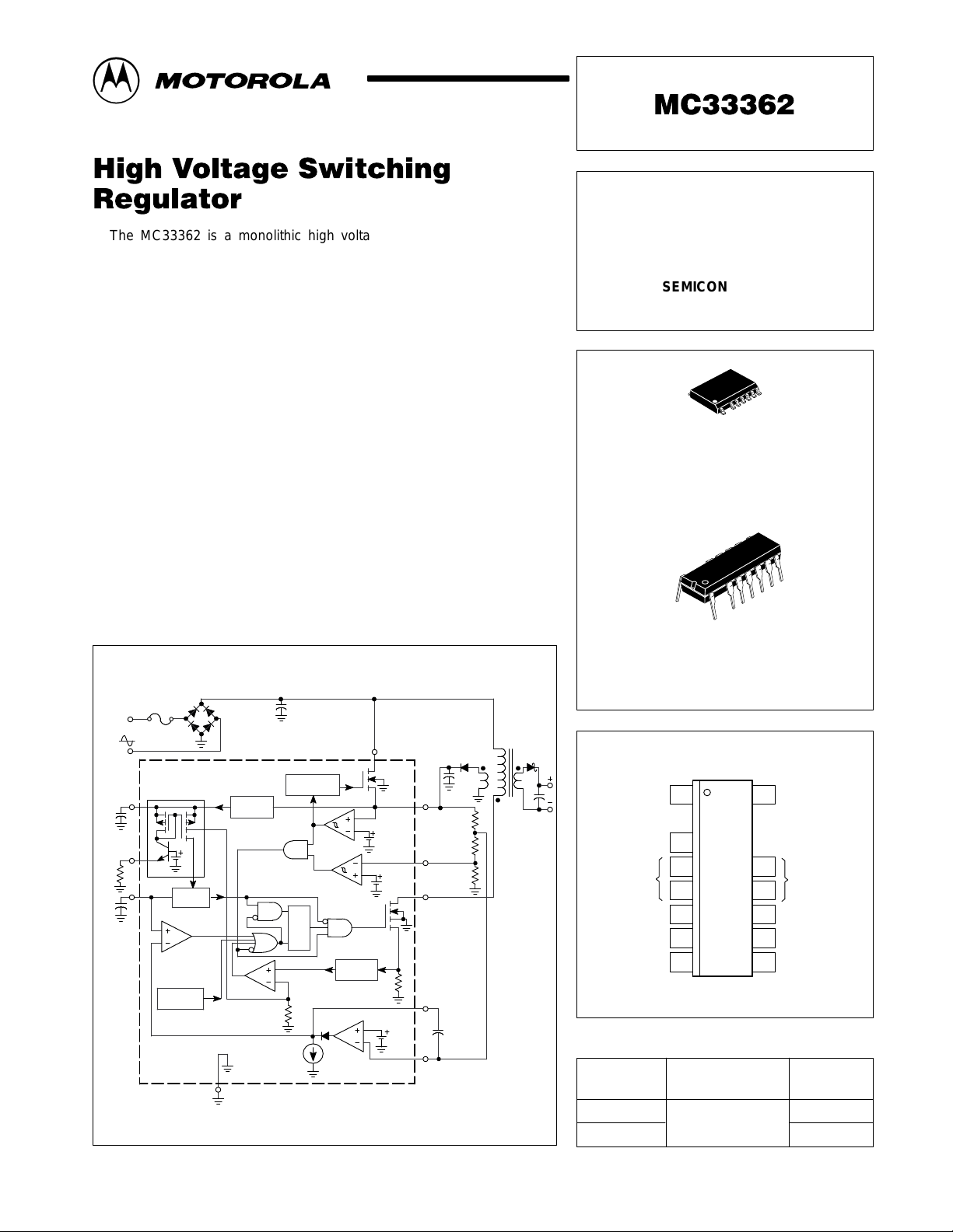
The MC33362 is a monolithic high voltage switching regulator that is
specifically designed to operate from a rectified 120 VAC line source. This
integrated circuit features an on–chip 500 V/2.0 A SenseFET power switch,
250 V active off–line startup FET, duty cycle controlled oscillator, current
limiting comparator with a programmable threshold and leading edge
blanking, latching pulse width modulator for double pulse suppression, high
gain error amplifier, and a trimmed internal bandgap reference. Protective
features include cycle–by–cycle current limiting, input undervoltage lockout
with hysteresis, output overvoltage protection, and thermal shutdown. This
device is available in a 16–lead dual–in–line and wide body surface mount
packages.
• On–Chip 500 V, 2.0 A SenseFET Power Switch
• Rectified 120 V AC Line Source Operation
• On–Chip 250 V Active Off–Line Startup FET
• Latching PWM for Double Pulse Suppression
• Cycle–By–Cycle Current Limiting
• Input Undervoltage Lockout with Hysteresis
• Output Overvoltage Protection Comparator
• Trimmed Internal Bandgap Reference
• Internal Thermal Shutdown
Simplified Application
HIGH VOLTAGE
OFF–LINE
SWITCHING REGULATOR
SEMICONDUCTOR
TECHNICAL DATA
16
1
DW SUFFIX
PLASTIC PACKAGE
CASE 751N
(SOP–16L)
16
1
P SUFFIX
PLASTIC PACKAGE
CASE 648E
(DIP–16)
AC Input
Startup Input
Regulator
Output
8
6
R
T
C
7
T
Mirror
Reg
Osc
PWM
Thermal
Gnd 4, 5, 12, 13
This device contains 221 active transistors.
Startup
PWM Latch
S
Q
R
I
pk
Driver
EA
MOTOROLA ANALOG IC DEVICE DATA
LEB
1
UVLO
OVP
V
CC
3
Overvoltage
Protection
Input
11
16
Power Switch
Drain
Compensation
9
10
Voltage
Feedback
Input
DC Output
PIN CONNECTIONS
Startup Input
V
CC
Gnd
R
T
C
T
Regulator Output
116
3
4
5
6
7
8
(Top View)
Power Switch
Drain
13
Gnd
12
Overvoltage
11
Protection Input
Voltage Feedback
10
Input
Compensation
9
ORDERING INFORMATION
Operating
Device
MC33362DW
MC33362P DIP–16
Motorola, Inc. 1999 Rev 3
Temperature Range
TJ = –25° to +125°C
Package
SOP–16L
1
Page 2
MAXIMUM RATINGS
Á
Á
Á
Á
Á
Á
Á
Á
Á
Á
Á
Á
Á
Á
Á
Á
Á
Á
Á
Á
Á
Á
Á
Á
Á
Á
Á
Á
Á
Á
Á
Á
Á
Á
Á
Á
Á
Á
Á
Á
Á
Á
Á
Á
Á
Á
Á
Á
Á
ÁÁÁ
Á
Á
Á
Á
Á
Á
ÁÁÁ
Á
Á
Á
Á
Á
Á
ÁÁÁ
Á
Á
Á
Á
Á
Á
ÁÁÁ
Á
Á
Á
Á
Á
Á
Á
Á
Á
Á
Á
Á
Á
Á
Á
Á
Á
Á
Á
Á
Á
ÁÁÁ
Á
Á
Á
Á
ÁÁÁ
ÁÁÁ
ÁÁÁ
ÁÁÁ
ÁÁÁ
ÁÁÁ
Rating Symbol Value Unit
Power Switch (Pin 16)
Drain Voltage
ББББББББББББ
Drain Current
Startup Input Voltage (Pin 1, Note 1)
ББББББББББББ
Pin 3 = Gnd
Pin 3 ≤ 1000 µF to ground
ББББББББББББ
Power Supply Voltage (Pin 3)
Input Voltage Range
Voltage Feedback Input (Pin 10)
ББББББББББББ
Compensation (Pin 9)
Overvoltage Protection Input (Pin 11)
ББББББББББББ
RT (Pin 6)
ББББББББББББ
CT (Pin 7)
Thermal Characteristics
P Suffix, Dual–In–Line Case 648E
ББББББББББББ
Thermal Resistance, Junction–to–Air
Thermal Resistance, Junction–to–Case
ББББББББББББ
(Pins 4, 5, 12, 13)
DW Suffix, Surface Mount Case 751N
Thermal Resistance, Junction–to–Air
ББББББББББББ
Thermal Resistance, Junction–to–Case
ББББББББББББ
(Pins 4, 5, 12, 13)
Refer to Figures 15 and 16 for additional thermal
ББББББББББББ
information.
Operating Junction Temperature
Storage Temperature
NOTE: ESD data available upon request.
MC33362
V
DS
ÁÁ
I
DS
V
in
ÁÁ
ÁÁ
V
CC
V
IR
ÁÁ
ÁÁ
ÁÁ
ÁÁ
R
θJA
R
ÁÁ
θJC
R
ÁÁ
θJA
R
θJC
ÁÁ
ÁÁ
T
J
T
stg
500
ÁÁÁ
2.0
ÁÁÁ
250
400
ÁÁÁ
40
–1.0 to V
ÁÁÁ
ÁÁÁ
ÁÁÁ
ÁÁÁ
ÁÁÁ
ÁÁÁ
ÁÁÁ
ÁÁÁ
reg
80
15
95
15
– 25 to +150
– 55 to +150
V
Á
A
V
Á
Á
V
V
Á
Á
Á
°C/W
Á
Á
Á
Á
Á
°C
°C
ELECTRICAL CHARACTERISTICS (V
= 20 V, RT = 10 k, CT = 390 pF, C
CC
= 1.0 µF, for typical values TJ = 25°C,
Pin 8
for min/max values TJ is the operating junction temperature range that applies (Note 2), unless otherwise noted.)
Characteristic
Symbol Min Typ Max Unit
REGULAT OR (Pin 8)
Output Voltage (IO = 0 mA, TJ = 25°C)
БББББББББББББББББ
Line Regulation (VCC = 20 V to 40 V)
БББББББББББББББББ
Load Regulation (IO = 0 mA to 10 mA)
БББББББББББББББББ
Total Output Variation over Line, Load, and Temperature
БББББББББББББББББ
OSCILLAT OR (Pin 7)
ББББББББББББББББББББББББББББББББ
Frequency
БББББББББББББББББ
CT = 390 pF
TJ = 25°C (VCC = 20 V)
БББББББББББББББББ
TJ = T
БББББББББББББББББ
CT = 2.0 nF
TJ = 25°C (VCC = 20 V)
БББББББББББББББББ
TJ = T
low
low
to T
to T
(VCC = 20 V to 40 V)
high
(VCC = 20 V to 40 V)
high
Frequency Change with Voltage (VCC = 20 V to 40 V)
V
reg
ÁÁÁ
Reg
line
ÁÁÁ
Reg
load
ÁÁÁ
V
reg
ÁÁÁ
f
OSC
ÁÁÁ
ÁÁÁ
ÁÁÁ
ÁÁÁ
∆f
/∆V
OSC
5.5
ÁÁ
–
ÁÁ
–
ÁÁ
5.3
ÁÁ
ÁÁ
260
ÁÁ
255
ÁÁ
60
ÁÁ
59
–
6.5
ÁÁ
30
ÁÁ
44
ÁÁ
–
ÁÁ
ÁÁ
285
ÁÁ
–
ÁÁ
67.5
ÁÁ
–
0.1
7.5
ÁÁ
500
ÁÁ
200
ÁÁ
8.0
ÁÁ
ÁÁ
310
ÁÁ
315
ÁÁ
75
ÁÁ
76
2.0
ERROR AMPLIFIER (Pins 9, 10)
Voltage Feedback Input Threshold
Line Regulation (VCC = 20 V to 40 V, TJ = 25°C)
Input Bias Current (VFB = 2.6 V)
Open Loop Voltage Gain (TJ= 25°C)
Gain Bandwidth Product (f = 100 kHz, TJ= 25°C)
NOTES: 1. Maximum power dissipation limits must be observed.
2.Tested junction temperature range for the MC33362:
T
= –25°CT
low
2
high
= +125°C
V
Reg
A
GBW
FB
line
I
IB
VOL
2.52
–
–
–
–
2.6
0.6
20
82
1.0
2.68
5.0
500
–
–
MOTOROLA ANALOG IC DEVICE DATA
V
ÁÁ
mV
ÁÁ
mV
ÁÁ
V
ÁÁ
kHz
ÁÁ
ÁÁ
ÁÁ
ÁÁ
kHz
V
mV
nA
dB
MHz
Page 3
MC33362
Á
Á
Á
Á
Á
ÁÁÁ
Á
ÁÁÁ
ÁÁÁ
Á
Á
Á
Á
Á
ÁÁÁ
Á
Á
Á
Á
Á
Á
Á
Á
Á
Á
Á
ÁÁÁ
Á
Á
Á
Á
Á
Á
Á
ÁÁÁ
Á
Á
Á
Á
Á
Á
ÁÁÁ
Á
Á
Á
Á
Á
Á
ÁÁÁ
Á
ÁÁÁ
Á
Á
Á
Á
Á
Á
Á
Á
Á
Á
ÁÁÁ
Á
Á
ÁÁÁ
ÁÁÁ
ÁÁÁ
Á
Á
Á
Á
Á
Á
Á
Á
Á
Á
ÁÁÁ
Á
Á
ELECTRICAL CHARACTERISTICS (continued) (V
= 20 V, RT = 10 k, CT = 390 pF, C
CC
= 1.0 µF, for typical values TJ = 25°C,
Pin 8
for min/max values TJ is the operating junction temperature range that applies (Note 2), unless otherwise noted.)
Characteristic UnitMaxTypMinSymbol
ERROR AMPLIFIER (Pins 9, 10)
Output Voltage Swing
High State (I
БББББББББББББББББ
Low State (I
= 100 µA, VFB < 2.0 V)
Source
= 100 µA, V
Sink
> 3.0 V)
FB
V
OH
ÁÁÁ
V
OL
4.0
ÁÁ
–
5.3
ÁÁ
0.2
–
ÁÁ
0.35
V
ÁÁ
OVERVOLTAGE DETECTION (Pin 11)
Input Threshold Voltage
Input Bias Current (Vin = 2.6 V)
V
th
I
IB
2.47
–
2.6
100
2.73
500
V
nA
PWM COMPARATOR (Pins 7, 9)
Duty Cycle
Maximum (VFB = 0 V)
БББББББББББББББББ
Minimum (VFB = 2.7 V)
DC
(max)
ÁÁÁ
DC
(min)
48
ÁÁ
–
50
ÁÁ
0
52
ÁÁ
0
%
ÁÁ
POWER SWITCH (Pin 16)
Drain–Source On–State Resistance (ID = 200 mA)
БББББББББББББББББ
TJ = 25°C
TJ = T
БББББББББББББББББ
Drain–Source Off–State Leakage Current (VDS = 500 V)
БББББББББББББББББ
Rise Time
БББББББББББББББББ
Fall Time
БББББББББББББББББ
OVERCURRENT COMPARATOR (Pin 16)
ББББББББББББББББББББББББББББББББ
Current Limit Threshold (RT = 10 k)
БББББББББББББББББ
low
to T
high
R
DS(on)
ÁÁÁ
ÁÁÁ
I
D(off)
ÁÁÁ
t
r
ÁÁÁ
t
f
ÁÁÁ
I
lim
ÁÁÁ
ÁÁ
–
–
ÁÁ
–
ÁÁ
–
ÁÁ
–
ÁÁ
0.7
ÁÁ
ÁÁ
4.4
–
ÁÁ
0.2
ÁÁ
50
ÁÁ
50
ÁÁ
0.9
ÁÁ
ÁÁ
6.0
12
ÁÁ
50
ÁÁ
–
ÁÁ
–
ÁÁ
1.1
ÁÁ
Ω
ÁÁ
ÁÁ
µA
ÁÁ
ns
ÁÁ
ns
ÁÁ
A
ÁÁ
STARTUP CONTROL (Pin 1)
Peak Startup Current (Vin = 200 V)
БББББББББББББББББ
VCC = 0 V
VCC = (V
БББББББББББББББББ
th(on)
– 0.2 V)
Off–State Leakage Current (Vin = 50 V, VCC = 20 V)
I
start
ÁÁÁ
ÁÁÁ
I
D(off)
ÁÁ
–
–
ÁÁ
–
ÁÁ
55
26
ÁÁ
40
ÁÁ
–
–
ÁÁ
200
mA
ÁÁ
ÁÁ
µA
UNDERVOLTAGE LOCKOUT (Pin 3)
Startup Threshold (VCC Increasing)
Minimum Operating Voltage After Turn–On
V
th(on)
V
CC(min)
11
7.5
14.5
9.5
18
11.5
V
V
TOTAL DEVICE (Pin 3)
Power Supply Current
БББББББББББББББББ
Startup (V
Operating
БББББББББББББББББ
= 10 V, Pin 1 Open)
CC
I
CC
ÁÁÁ
ÁÁÁ
ÁÁ
–
–
ÁÁ
ÁÁ
0.3
3.6
ÁÁ
ÁÁ
0.5
5.0
ÁÁ
mA
ÁÁ
ÁÁ
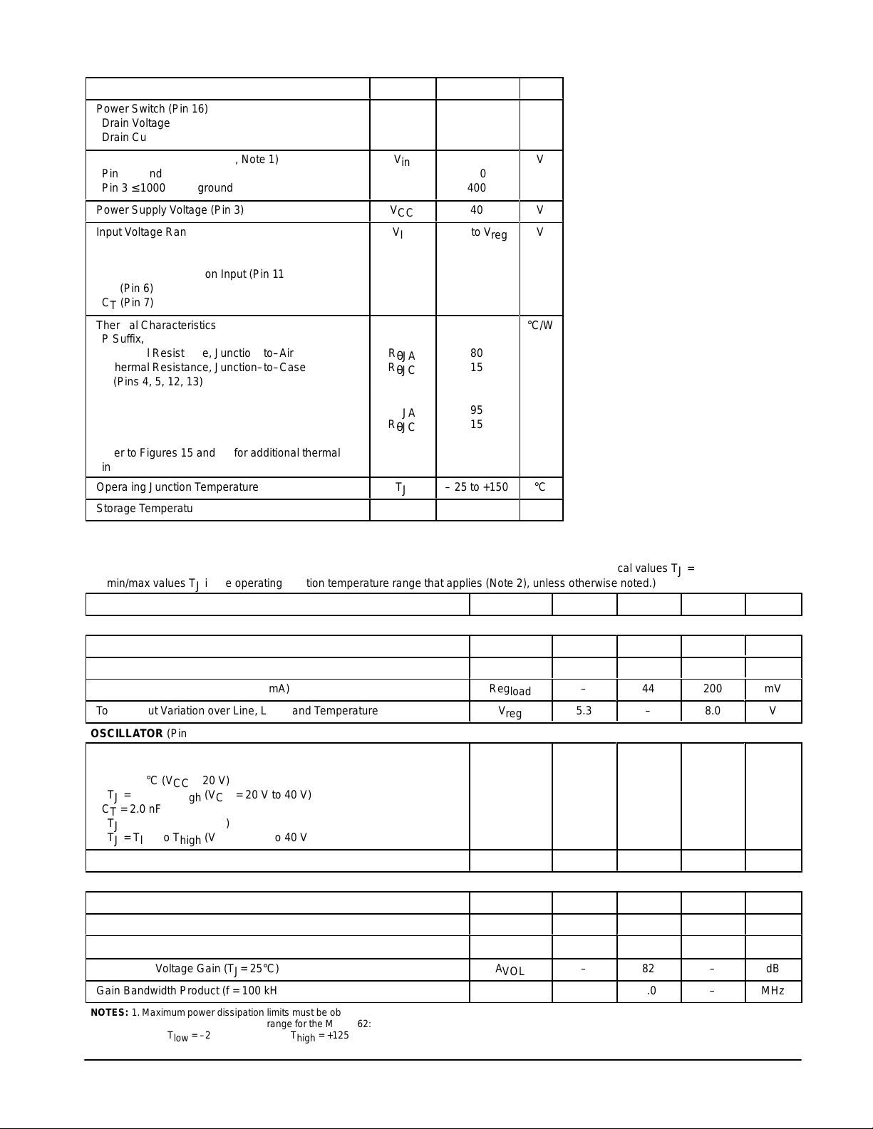
Figure 1. Oscillator Frequency
versus Timing Resistor
1.0 M
CT = 200 pF
500 k
CT = 500 pF
200 k
CT = 1.0 nF
100 k
CT = 2.0 nF
50 k
CT = 5.0 nF
, OSCILLAT OR FREQUENCY (Hz)
20 k
OSC
CT = 10 nF
f
10 k
5.0
10 15 20 30 50 7.0 10 15 20 30 40 50
RT, TIMING RESISTOR (kΩ)
MOTOROLA ANALOG IC DEVICE DATA
CT = 100 pF
VCC = 20 V
°
C
TA = 25
Figure 2. Power Switch Peak Drain Current
versus Timing Resistor
2.0
1.5
1.0
0.8
0.6
0.4
Inductor supply voltage and inductance value are
adjusted so that Ipk turn–off is achieved at 5.0
, POWER SWITCH PEAK DRAIN CURRENT (A)
0.2
PK
5.0
I
RT, TIMING RESISTOR (kΩ)
µ
s.
VCC = 20 V
µ
CT = 1.0
°
C
TA = 25
3
F
Page 4
MC33362
, OSCILLAT OR
dscg
/I
chg
I
1.0
0.7
0.5
0.3
0.2
0.15
CHARGE/DISCHARGE CURRENT (mA)
0.1
100
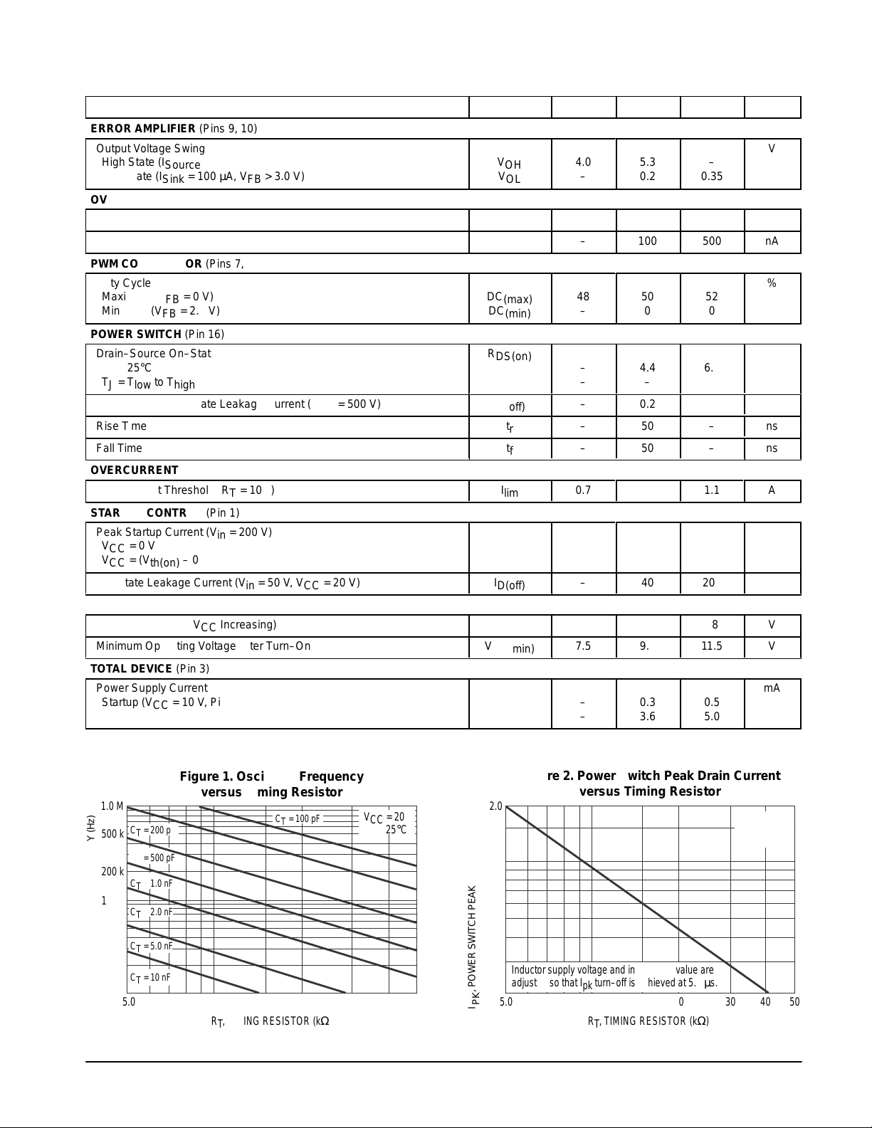
Figure 3. Oscillator Charge/Discharge
Current versus Timing Resistor
5.0
10 15 20 30 50 2.0 3.0 5.0 7.0 10
RT, TIMING RESISTOR (kΩ)
Figure 5. Error Amp Open Loop Gain and
Phase versus Frequency
80
Gain
60
Phase
40
VCC = 20 V
°
C
TA = 25
VCC = 20 V
VO = 1.0 to 4.0 V
RL = 5.0 M
CL = 2.0 pF
TA = 25
Ω
°
C
0
30
60
90
70
60
50
40
, MAXIMUM OUTPUT DUTY CYCLE (%)
max
D
30
1.0
0
–1.0
– 2.0
Figure 4. Maximum Output Duty Cycle
versus Timing Resistor Ratio
RD/RT Ratio
Discharge Resistor
Pin 6 to Gnd
TIMING RESISTOR RA TIO
VCC = 20 V
CT = 2.0 nF
TA = 25
RC/RT Ratio
Charge Resistor
Pin 6 to V
Figure 6. Error Amp Output Saturation
V oltage versus Load Current
Source Saturation)
(Load to Ground)
V
ref
reg
°
C
20
, OPEN LOOP VOL TAGE GAIN (dB)
0
VOL
A
–20
10
Figure 7. Error Amplifier Small Signal
1.80 V
1.75 V
1.70 V
, OUTPUT SA TURATION VOLTAGE (V)
V
sat
2.0
1.0
Sink Saturation
(Load to V
0
0
IO, OUTPUT LOAD CURRENT (mA)
ref
)
Gnd
VCC = 20 V
°
C
TA = 25
120
, EXCESS PHASE (DEGREES)
θ
150
100 1.0 k 10 k 100 k 1.0 M 10 M 0.2 0.4 0.6 0.8 1.0
f, FREQUENCY (Hz)
180
Figure 8. Error Amplifier Large Signal
Transient Response
1.0 µs/DIV
VCC = 20 V
AV = –1.0
CL = 10 pF
°
C
TA = 25
3.00 V
1.75 V
20 mV/DIV
0.50 V
Transient Response
1.0 µs/DIV
VCC = 20 V
AV = –1.0
CL = 10 pF
°
C
TA = 25
0.5 V/DIV
4
MOTOROLA ANALOG IC DEVICE DATA
Page 5

MC33362
Figure 9. Regulator Output Voltage
Change versus Source Current
0
–20
–40
–60
, REGULAT OR VOLTAGE CHANGE (mV)
reg
V
–80
∆
0
4.0 8.0 12 16 20 2.0 4.0 6.0 8.0 10 12 14
I
reg
Figure 11. Power Switch Drain–Source
Ω
10
8.0
On–Resistance versus T emperature
ID = 200 mA
VCC = 20 V
RT = 10 k
C
= 1.0
PIN 8
°
C
TA = 25
, REGULAT OR SOURCE CURRENT (mA)
Figure 10. Peak Startup Current
versus Power Supply V oltage
60
µ
F
40
20
Pulse tested with an on–time of 20 µs to 300 µs
, PEAK STARTUP CURRENT (mA)
at < 1.0% duty cycle. The on–time is adjusted at
pk
Pin 1 for a maximum peak current out of Pin 3.
I
0
0
VCC, POWER SUPPLY VOLTAGE (V)
V
Pin 1
TA = 25
= 200 V
°
C
Figure 12. Power Switch
Drain–Source Capacitance versus V oltage
200
150
VCC = 20 V
°
C
TA = 25
6.0
4.0
2.0
, DRAIN–SOURCE ON–RESISTANCE ( )
0
DS(on)
R
–50
–25 0 25 50 75 150100 5.0 50 500
Pulse tested at 5.0 ms with < 1.0% duty cycle
so that TJ is as close to TA as possible.
TA, AMBIENT TEMPERATURE (°C)
Figure 13. Supply Current versus Supply V oltage
4.0
CT = 390 pF
3.2
CT = 2.0 nF
2.4
1.6
, SUPPLY CURRENT (mA)
0.8
CC
I
0
0
10 20 30 40
VCC, SUPPLY VOLTAGE (V)
RT = 10 k
Pin 1 = Open
Pin 4, 5, 10, 11,
12, 13 = Gnd
TA = 25
125
°
C
100
50
, DRAIN–SOURCE CAPACITANCE (pF)
OSS
C
0
0.5
100
°
10
, THERMAL RESISTANCE
JA
JUNCTION–TO–AIR ( C/W)
θ
R
1.0
0.01
C
measured at 1.0 MHz with 50 mVpp.
OSS
VDS, DRAIN–SOURCE VOLTAGE (V)
Figure 14. DW and P Suffix Transient
Thermal Resistance
L = 12.7 mm of 2.0 oz.
copper. Refer to Figures
15 and 16.
0.1 1.0 10 100
t, TIME (s)
MOTOROLA ANALOG IC DEVICE DATA
5
Page 6

MC33362
Á
Á
Á
Á
Á
Á
Á
Á
Á
Á
Á
Á
Á
Á
Á
Á
Á
Á
Á
Á
Á
Á
Á
Á
Á
Á
Á
Á
Á
Á
Á
Á
Á
Á
Á
Á
Figure 15. DW Suffix (SOP–16L) Thermal Resistance and
Maximum Power Dissipation versus P.C.B. Copper Length
3.0 mm
2.8
2.4
2.0
1.6
1.2
0.8
0.4
0
100
90
80
°
70
60
, THERMAL RESISTANCE
50
JA
JUNCTION–TO–AIR ( C/W)
θ
R
40
30
0
°
P
D(max)
for TA = 50
C
Printed circuit board heatsink example
2.0 oz
L
Copper
L
Graphs represent symmetrical layout
R
θ
JA
10 20 30 40 50
L, LENGTH OF COPPER (mm)
PIN FUNCTION DESCRIPTION
Pin Function Description
1
ÁÁÁ
ÁÁÁ
2
3
ÁÁÁ
ÁÁÁ
4, 5, 12, 13
6
ÁÁÁ
7
ÁÁÁ
8
9
ÁÁÁ
10
ÁÁÁ
11
ÁÁÁ
ÁÁÁ
14, 15
ÁÁÁ
16
ÁÁÁ
Startup Input
ÁÁÁÁ
ÁÁÁÁ
–
V
CC
ÁÁÁÁ
ÁÁÁÁ
Ground
R
T
ÁÁÁÁ
C
T
ÁÁÁÁ
Regulator Output
Compensation
ÁÁÁÁ
Voltage Feedback
Input
ÁÁÁÁ
Overvoltage
ÁÁÁÁ
Protection Input
ÁÁÁÁ
–
ÁÁÁÁ
Power Switch
Drain
ÁÁÁÁ
This pin connects directly to the rectified ac line voltage source. Internally Pin 1 is tied to the drain
БББББББББББББББББББББББ
of a high voltage startup MOSFET. During startup, the MOSFET supplies internal bias, and charges
an external capacitor that connects from the V
БББББББББББББББББББББББ
This pin has been omitted for increased spacing between the rectified AC line voltage on Pin 1 and
the VCC potential on Pin 3.
This is the positive supply voltage input. During startup, power is supplied to this input from Pin 1.
БББББББББББББББББББББББ
When VCC reaches the UVLO upper threshold, the startup MOSFET turns off and power is supplied
from an auxiliary transformer winding.
БББББББББББББББББББББББ
These pins are the control circuit grounds. They are part of the IC lead frame and provide a thermal
path from the die to the printed circuit board.
Resistor RT connects from this pin to ground. The value selected will program the Current Limit
БББББББББББББББББББББББ
Comparator threshold and affect the Oscillator frequency.
Capacitor C
programs the Oscillator frequency.
БББББББББББББББББББББББ
connects from this pin to ground. The value selected, in conjunction with resistor R
T
This 6.5 V output is available for biasing external circuitry. It requires an external bypass capacitor
of at least 1.0 µF for stability.
This pin is the Error Amplifier output and is made available for loop compensation. It can be used as
БББББББББББББББББББББББ
an input to directly control the PWM Comparator.
This is the inverting input of the Error Amplifier. It has a 2.6 V threshold and normally connects
through a resistor divider to the converter output, or to a voltage that represents the converter
БББББББББББББББББББББББ
output.
This input provides runaway output voltage protection due to an external component or connection
БББББББББББББББББББББББ
failure in the control loop feedback signal path. It has a 2.6 V threshold and normally connects
through a resistor divider to the converter output, or to a voltage that represents the converter
БББББББББББББББББББББББ
output.
These pins have been omitted for increased spacing between the high voltages present on the
БББББББББББББББББББББББ
Power Switch Drain, and the ground potential on Pins 12 and 13.
This pin is designed to directly drive the converter transformer and is capable of switching a
maximum of 500 V and 2.0 A.
БББББББББББББББББББББББ
Figure 16. P Suffix (DIP–16) Thermal Resistance and
Maximum Power Dissipation versus P.C.B. Copper Length
JA
θ
R , THERMAL RESIST ANCE
, MAXIMUM POWER DISSIPATION (W)
D
P
100
80
°
60
40
20
JUNCTION–TO–AIR ( C/W)
0
0
CC
R
θ
JA
P
for TA = 70°C
D(max)
10 20 30 40 50
L, LENGTH OF COPPER (mm)
pin to ground.
Printed circuit board heatsink example
2.0 oz
L
Copper
L
Graphs represent symmetrical layout
3.0 mm
5.0
4.0
3.0
2.0
1.0
0
,
T
, MAXIMUM POWER DISSIPATION (W)
D
P
6
MOTOROLA ANALOG IC DEVICE DATA
Page 7

AC Input
MC33362
Figure 17. Representative Block Diagram
Regulator Output
6.5 V
8
6
R
T
C
7
T
I
Current
Mirror
4 I
Oscillator
PWM
Comparator
Thermal
Shutdown
2.25 I
Band Gap
Regulator
PWM Latch
Current Limit
Comparator
4, 5, 12, 13Gnd
S
Q
R
450
270µA
Startup Input
Startup
Control
UVLO
OVP
Driver
Leading Edge
Blanking
Error
Amplifier
1
14.5 V/
9.5 V
2.6 V
2.6 V
V
CC
3
Overvoltage
Protection
Input
11
16
Power Switch
Drain
9.0
Compensation
9
10
Voltage
Feedback Input
DC Output
Capacitor C
Compensation
Oscillator Output
Power Switch
Leading Edge
Blanking Input
(Power Switch
Drain Current)
T
PWM
Comparator
Output
PWM Latch
Q Output
Gate Drive
Figure 18. Timing Diagram
2.6 V
0.6 V
Current Limit
Propagation
Delay
Current
Limit
Threshold
Normal PWM Operating Range Output Overload
MOTOROLA ANALOG IC DEVICE DATA
7
Page 8

MC33362
OPERA TING DESCRIPTION
Introduction
The MC33362 represents a new higher level of integration
by providing all the active high voltage power, control, and
protection circuitry required for implementation of a flyback or
forward converter on a single monolithic chip. This device is
designed for direct operation from a rectified 120 VAC line
source and requires a minimum number of external
components to implement a complete converter. A
description of each of the functional blocks is given below,
and the representative block and timing diagrams are shown
in Figures 17 and 18.
Oscillator and Current Mirror
The oscillator frequency is controlled by the values
selected for the timing components R
and CT. Resistor R
T
programs the oscillator charge/discharge current via the
Current Mirror 4 I output, Figure 3. Capacitor C
is charged
T
and discharged by an equal magnitude internal current
source and sink. This generates a symmetrical 50 percent
duty cycle waveform at Pin 7, with a peak and valley
threshold of 2.6 V and 0.6 V respectively. During the
discharge of C
, the oscillator generates an internal blanking
T
pulse that holds the inverting input of the AND gate Driver
high. This causes the Power Switch gate drive to be held in a
low state, thus producing a well controlled amount of output
deadtime. The amount of deadtime is relatively constant with
respect to the oscillator frequency when operating below
1.0 MHz. The maximum Power Switch duty cycle at Pin 16
can be modified from the internal 50% limit by providing an
additional charge or discharge current path to C
, Figure 19.
T
In order to increase the maximum duty cycle, a discharge
current resistor R
is connected from Pin 7 to ground. To
D
decrease the maximum duty cycle, a charge current resistor
R
is connected from Pin 7 to the Regulator Output. Figure 4
C
shows an obtainable range of maximum output duty cycle
versus the ratio of either R
or R
C
with respect to RT.
D
Figure 19. Maximum Duty Cycle Modification
Current
Regulator Output
1.0
R
C
R
T
C
R
D
T
8
6
7
Mirror
2.25 I
I
Current
Limit
Reference
4 I
Oscillator
Blanking
Pulse
The formula for the charge/discharge current along with
the oscillator frequency are given below. The frequency
formula is a first order approximation and is accurate for C
values greater than 500 pF. For smaller values of CT, refer to
Figure 1. Note that resistor R
also programs the Current
T
Limit Comparator threshold.
I
chgńdscg
+
5.4
R
T
f
I
[
chgńdscg
PWM Comparator and Latch
The pulse width modulator consists of a comparator with
the oscillator ramp voltage applied to the non–inverting input,
while the error amplifier output is applied into the inverting
T
input. The Oscillator applies a set pulse to the PWM Latch
while C
is discharging, and upon reaching the valley
T
voltage, Power Switch conduction is initiated. When C
charges to a voltage that exceeds the error amplifier output,
the PWM Latch is reset, thus terminating Power Switch
conduction for the duration of the oscillator ramp–up period.
This PWM Comparator/Latch combination prevents multiple
output pulses during a given oscillator clock cycle. The timing
diagram shown in Figure 18 illustrates the Power Switch duty
cycle behavior versus the Compensation voltage.
Current Limit Comparator and Power Switch
The MC33362 uses cycle–by–cycle current limiting as a
means of protecting the output switch transistor from
overstress. Each on–cycle is treated as a separate situation.
Current limiting is implemented by monitoring the output
switch current buildup during conduction, and upon sensing
an overcurrent condition, immediately turning off the switch
for the duration of the oscillator ramp–up period.
The Power Switch is constructed as a SenseFET allowing
a virtually lossless method of monitoring the drain current. It
consists of a total of 3770 cells, of which 50 are connected to
a 9.0 Ω ground–referenced sense resistor. The Current
Sense Comparator detects if the voltage across the sense
resistor exceeds the reference level that is present at the
inverting input. If exceeded, the comparator quickly resets
the PWM Latch, thus protecting the Power Switch. The
current limit reference level is generated by the 2.25 I output
of the Current Mirror. This current causes a reference voltage
to appear across the 450 Ω resistor. This voltage level, as
well as the Oscillator charge/discharge current are both set
by resistor R
. Therefore when selecting the values for R
T
and CT, RT must be chosen first to set the Power Switch peak
drain current, while C
is chosen second to set the desired
T
Oscillator frequency . A graph of the Power Switch peak drain
current versus R
is shown in Figure 2 with the related
T
formula below.
4C
T
T
T
T
R
– 1.1 15
T
ǒ
PWM
Comparator
Ipk+
8
12.3
MOTOROLA ANALOG IC DEVICE DATA
1000
Ǔ
Page 9

MC33362
The Power Switch is designed to directly drive the converter
transformer and is capable of switching a maximum of 500 V
and 2.0 A. Proper device voltage snubbing and heatsinking
are required for reliable operation.
A Leading Edge Blanking circuit was placed in the current
sensing signal path. This circuit prevents a premature reset
of the PWM Latch. The premature reset is generated each
time the Power Switch is driven into conduction. It appears as
a narrow voltage spike across the current sense resistor, and
is due to the MOSFET gate to source capacitance,
transformer interwinding capacitance, and output rectifier
recovery time. The Leading Edge Blanking circuit has a
dynamic behavior in that it masks the current signal until the
Power Switch turn–on transition is completed. The current
limit propagation delay time is typically 233 ns. This time is
measured from when an overcurrent appears at the Power
Switch drain, to the beginning of turn–off.
Error Amplifier
An fully compensated Error Amplifier with access to the
inverting input and output is provided for primary side voltage
sensing, Figure 17. It features a typical dc voltage gain of 82
dB, and a unity gain bandwidth of 1.0 MHz with 78 degrees of
phase margin, Figure 5. The noninverting input is internally
biased at 2.6 V ±3.1% and is not pinned out. The Error
Amplifier output is pinned out for external loop compensation
and as a means for directly driving the PWM Comparator.
The output was designed with a limited sink current capability
of 270 µA, allowing it to be easily overridden with a pull–up
resistor. This is desirable in applications that require
secondary side voltage sensing, Figure 20. In this
application, the Voltage Feedback Input is connected to the
Regulator Output. This disables the Error Amplifier by placing
its output into the sink state, allowing the optocoupler
transistor to directly control the PWM Comparator.
Overvoltage Protection
An Overvoltage Protection Comparator is included to
eliminate the possibility of runaway output voltage. This
condition can occur if the control loop feedback signal path is
broken due to an external component or connection failure.
The comparator is normally used to monitor the primary side
V
voltage. When the 2.6 V threshold is exceeded, it will
CC
immediately turn off the Power Switch, and protect the load
from a severe overvoltage condition. This input can also be
driven from external circuitry to inhibit converter operation.
Undervoltage Lockout
An Undervoltage Lockout comparator has been
incorporated to guarantee that the integrated circuit has
sufficient voltage to be fully functional before the output stage
is enabled. The UVLO comparator monitors the V
CC
voltage
at Pin 3 and when it exceeds 14.5 V, the reset signal is
removed from the PWM Latch allowing operation of the
Power Switch. T o prevent erratic switching as the threshold is
crossed, 5.0 V of hysteresis is provided.
Startup Control
An internal Startup Control circuit with a high voltage
enhancement mode MOSFET is included within the
MC33362. This circuitry allows for increased converter
efficiency by eliminating the external startup resistor, and its
associated power dissipation, commonly used in most
off–line converters that utilize a UC3842 type of controller.
Rectified ac line voltage is applied to the Startup Input, Pin 1.
This causes the MOSFET to enhance and supply internal
bias as well as charge current to the V
that connects from Pin 3 to ground. When V
bypass capacitor
CC
reaches the
CC
UVLO upper threshold of 14.5 V, the IC commences
operation and the startup MOSFET is turned off. Operating
bias is now derived from the auxiliary transformer winding,
and all of the device power is efficiently converted down from
the rectified ac line.
The startup MOSFET will provide an initial peak current of
55 mA, Figure 10, which decreases rapidly as V
and the
CC
die temperature rise. The steady state current will self limit in
the range of 12 mA with VCC shorted to ground. The startup
MOSFET is rated at a maximum of 250 V with V
ground, and 400 V when charging a V
shorted to
CC
capacitor of
CC
1000 µF or less.
Regulator
A low current 6.5 V regulated output is available for
biasing the Error Amplifier and any additional control system
circuitry. It is capable of up to 10 mA and has short–circuit
protection. This output requires an external bypass capacitor
of at least 1.0 µF for stability.
Thermal Shutdown and Package
Internal thermal circuitry is provided to protect the Power
Switch in the event that the maximum junction temperature is
exceeded. When activated, typically at 155°C, the Latch is
forced into a ‘reset’ state, disabling the Power Switch. The
Latch is allowed to ‘set’ when the Power Switch temperature
falls below 145°C. This feature is provided to prevent
catastrophic failures from accidental device overheating. It is
not intended to be used as a substitute for proper
heatsinking.
The MC33362 is contained in a heatsinkable plastic
dual–in–line package in which the die is mounted on a
special heat tab copper alloy lead frame. This tab consists of
the four center ground pins that are specifically designed to
improve thermal conduction from the die to the circuit board.
Figures 15 and 16 show a simple and effective method of
utilizing the printed circuit board medium as a heat dissipater
by soldering these pins to an adequate area of copper foil.
This permits the use of standard layout and mounting
practices while having the ability to halve the junction to air
thermal resistance. The examples are for a symmetrical
layout on a single–sided board with two ounce per square
foot of copper. Figure 22 shows a practical example of a
printed circuit board layout that utilizes the copper foil as a
heat dissipater. Note that a jumper was added to the layout
from Pins 8 to 10 in order to enhance the copper area near
the device for improved thermal conductivity. The application
circuit requires two ounce copper foil in order to obtain
20 watts of continuous output power at room temperature.
MOTOROLA ANALOG IC DEVICE DATA
9
Page 10

MC33362
Figure 20. 20 W Off–Line Converter
92 to 138
Vac Input
C4
1.0
R1
8.2 k
C3
1.5 nF
F1
1.0 A
8
6
7
D4
D2
D3
D1
Mirror
Osc
PWM
Thermal
1N4004
Reg
PWM Latch
270µA
C1
47
S
R
Q
I
Limit
Startup
Driver
LEB
EA
1
UVLO
14.5 V/
9.5 V
OVP
2.6 V
2.6 V
C5
4.0 nF
3
11
16
9
10
100 k
1.0 W
MUR
160
C2
10
R4
16 k
R3
2.7 k
5
4
R2
2.7 k
R6
D5
R5
39
C6
47 pF
R7
2.2 k
1.0 W
D6
MUR
120
T1
D7
MBR
2515L
MOC
8103
C8
330
IC2
C9
C10
330
330
IC3
TL431B
1
2
3
2
L1
µ
5.0
R8
220
R9
2.80 k
C7
100 nF
1
R10
2.74 k
H
5.05 V/4.0 A
DC Output
C11
220
C12
1.0
4, 5, 12, 13
IC1 MC33362
Figure 21. Converter T est Data
Test Conditions Results
Line Regulation Vin = 92 Vac to 138 Vac, IO 4.0 A ∆ = 1.0 mV
Load Regulation Vin = 115 Vac, IO = 1.0 A to 4.0 A ∆ = 9.0 mV
Output Ripple Vin = 115 Vac, IO = 4.0 A Triangular = 10 mVpp
Spike = 60 mVpp
Efficiency Vin = 115 Vac, IO = 4.0 A 78.4%
This data was taken with the components listed below mounted on the printed circuit board shown in Figure 22.
For high efficiency and small circuit board size, the Sanyo Os–Con capacitors are recommended for C8, C9, C10 and C11.
C8, C9, C10 = Sanyo Os–Con #6SA330M, 330 µF 6.3 V.
C11 = Sanyo Os–Con #10SA220M, 220 µF 10 V.
D7 = MBR2515L mounted on Aavid #592502B03400 heatsink.
L1 = Coilcraft S5088–A, 5.0 µH, 0.11 Ω.
T1 = Coilcraft S5069–A
Primary: 58 turns of # 26 AWG, Pin 1 = start, Pin 8 = finish.
Two layers 0.002″ Mylar tape.
Secondary: 4 turns of # 18 AWG, 2 strands bifiliar wound, Pin 5 = start, Pin 4 = finish.
Two layers 0.002″ Mylar tape.
Auxiliary: 10 turns of # 26 AWG wound in center of bobbin, Pin 2 = start, Pin 7 = finish.
Two layers 0.002″ Mylar tape.
Gap: 0.014″ total for a primary inductance (LP) of 330 µH.
Core and Bobbin: Coilcraft PT1950, E187, 3F3 material.
10
MOTOROLA ANALOG IC DEVICE DATA
Page 11
MC33362
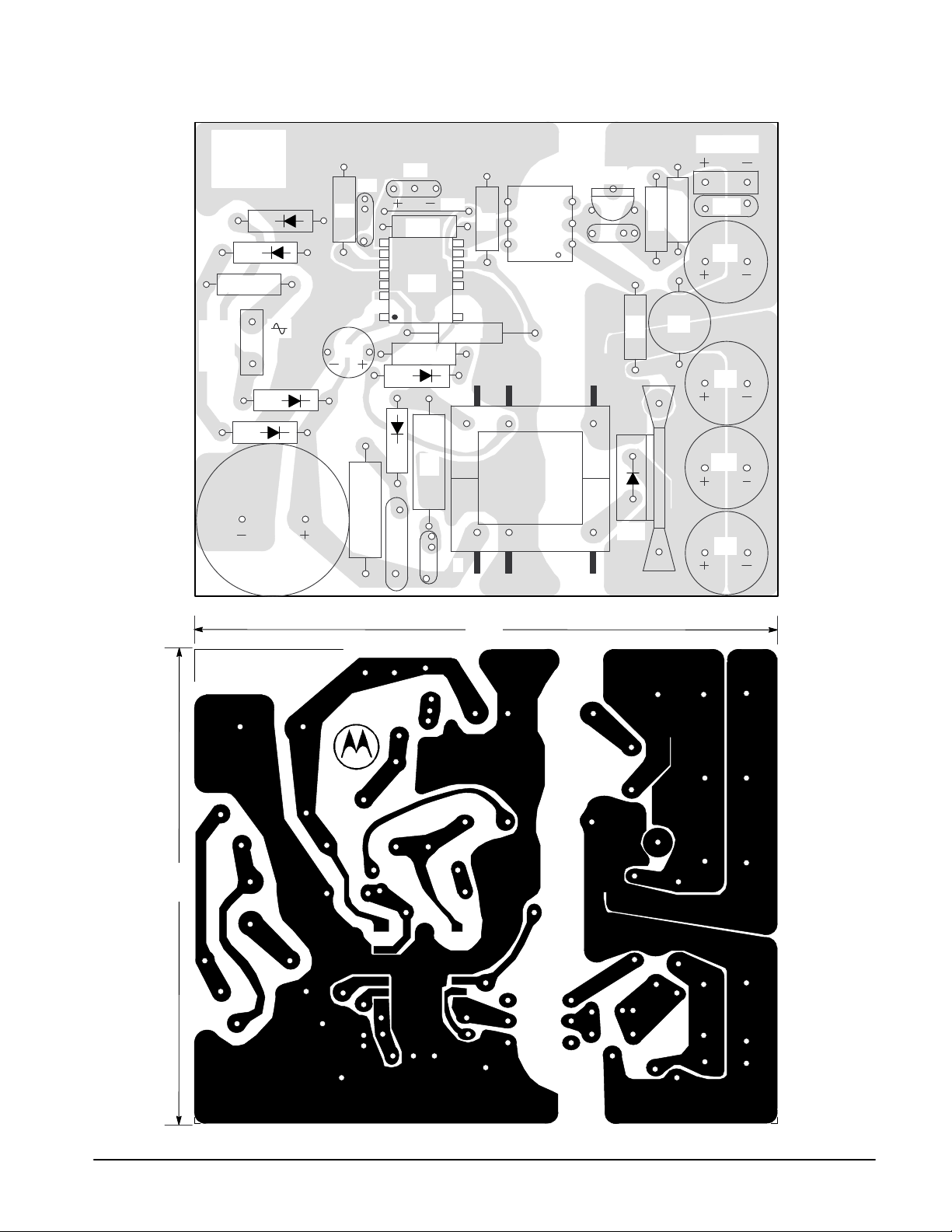
Figure 22. Printed Circuit Board and Component Layout
(Circuit of Figure 20)
Caution!
High
V oltages
AC
Line
Input
D2
F1
D4
D1
D3
C1
R1
C2
C3
R6
D6
D5
C5
C4
R2
IC1
R5
R7
C6
J1
DC Output
IC3
L1
R10
C12
C11
C10
C9
C8
R3
R3
R4
1
IC2
C7
T1
R9
R8
D7
MC33362
2.25”
(Top View)
2.75”
MOTOROLA ANALOG IC DEVICE DATA
(Bottom View)
11
Page 12

MC33362
OUTLINE DIMENSIONS
–A–
T
16 9
–B–
81
P
0.010 (0.25)
DW SUFFIX
PLASTIC PACKAGE
CASE 751N–01
(SOP–16L)
ISSUE O
M
M
B
J
D13X
0.010 (0.25) B
M
S
A
T
S
F
R
X 45
C
S
–T–
SEATING
PLANE
K
9X
G
M
P SUFFIX
PLASTIC PACKAGE
–A–
R
16 9
–B–
18
P
F
S
H
K
CASE 648E–01
(DIP–16)
ISSUE O
L
C
–T–
SEATING
PLANE
G
D
13 PL
0.25 (0.010) T
M
S
B
S
A
NOTES:
1. DIMENSIONING AND TOLERANCING PER ANSI
Y14.5M, 1982.
2. CONTROLLING DIMENSION: MILLIMETER.
3. DIMENSIONS A AND B DO NOT INCLUDE MOLD
PROTRUSION.
4. MAXIMUM MOLD PROTRUSION 0.15 (0.006) PER
SIDE.
5. DIMENSION D DOES NOT INCLUDE DAMBAR
PROTRUSION. ALLOWABLE DAMBAR
PROTRUSION SHALL BE 0.13 (0.005) TOTAL IN
EXCESS OF D DIMENSION AT MAXIMUM
MATERIAL CONDITION.
DIM MIN MAX MIN MAX
A 10.15 10.45 0.400 0.411
B 7.40 7.60 0.292 0.299
C 2.35 2.65 0.093 0.104
D 0.35 0.49 0.014 0.019
_
M
J
F 0.50 0.90 0.020 0.035
G 1.27 BSC 0.050 BSC
J 0.25 0.32 0.010 0.012
K 0.10 0.25 0.004 0.009
M 0 7 0 7
____
P 10.05 10.55 0.395 0.415
R 0.25 0.75 0.010 0.029
S 2.54 BSC 0.100 BSC
T 3.81 BSC 0.150 BSC
NOTES:
1. DIMENSIONING AND TOLERANCING PER ANSI
Y14.5M, 1982.
2. CONTROLLING DIMENSION: INCH.
3. DIMENSION L TO CENTER OF LEADS WHEN
FORMED PARALLEL.
4. DIMENSION A AND B DOES NOT INCLUDE MOLD
PROTRUSION.
5. MOLD FLASH OR PROTRUSIONS SHALL NOT
EXCEED 0.25 (0.010).
6. ROUNDED CORNER OPTIONAL.
DIM MIN MAX MIN MAX
A 0.740 0.760 18.80 19.30
B 0.245 0.260 6.23 6.60
C 0.145 0.175 3.69 4.44
D 0.015 0.021 0.39 0.53
F 0.050 0.070 1.27 1.77
G 0.100 BSC 2.54 BSC
H 0.050 BSC 1.27 BSC
J 0.008 0.015 0.21 0.38
K 0.120 0.140 3.05 3.55
L 0.295 0.305 7.50 7.74
M 0 10 0 10
____
P 0.200 BSC 5.08 BSC
R 0.300 BSC 7.62 BSC
S 0.015 0.035 0.39 0.88
INCHESMILLIMETERS
MILLIMETERSINCHES
Motorola reserves the right to make changes without further notice to any products herein. Motorola makes no warranty , representation or guarantee regarding
the suitability of its products for any particular purpose, nor does Motorola assume any liability arising out of the application or use of any product or circuit, and
specifically disclaims any and all liability, including without limitation consequential or incidental damages. “T ypical” parameters which may be provided in Motorola
data sheets and/or specifications can and do vary in different applications and actual performance may vary over time. All operating parameters, including “Typicals”
must be validated for each customer application by customer’s technical experts. Motorola does not convey any license under its patent rights nor the rights of
others. Motorola products are not designed, intended, or authorized for use as components in systems intended for surgical implant into the body, or other
applications intended to support or sustain life, or for any other application in which the failure of the Motorola product could create a situation where personal injury
or death may occur. Should Buyer purchase or use Motorola products for any such unintended or unauthorized application, Buyer shall indemnify and hold Motorola
and its officers, employees, subsidiaries, affiliates, and distributors harmless against all claims, costs, damages, and expenses, and reasonable attorney fees
arising out of, directly or indirectly, any claim of personal injury or death associated with such unintended or unauthorized use, even if such claim alleges that
Motorola was negligent regarding the design or manufacture of the part. Motorola and are registered trademarks of Motorola, Inc. Motorola, Inc. is an Equal
Opportunity/Affirmative Action Employer.
Mfax is a trademark of Motorola, Inc.
How to reach us:
USA/EUROPE/ Locations Not Listed: Motorola Literature Distribution; JAPAN: Motorola Japan Ltd.; SPD, Strategic Planning Office, 141,
P.O. Box 5405, Denver, Colorado 80217. 1–303–675–2140 or 1–800–441–2447 4–32–1 Nishi–Gotanda, Shinagawa–ku, Tokyo, Japan. 81–3–5487–8488
Customer Focus Center: 1–800–521–6274
Mfax: RMFAX0@email.sps.mot.com – TOUCHTONE 1–602–244–6609 ASIA/PACIFIC: Motorola Semiconductors H.K. Ltd.; Silicon Harbour Centre,
Motorola Fax Back System – US & Canada ONLY 1–800–774–1848 2, Dai King Street, Tai Po Industrial Estate, Tai Po, N.T., Hong Kong.
– http://sps.motorola.com/mfax/ 852–26629298
HOME PAGE: http://motorola.com/sps/
12
◊
MOTOROLA ANALOG IC DEVICE DATA
MC33362/D
 Loading...