

Page 1
MC33349
Lithium Battery Protection
Circuit for One Cell
Battery Packs
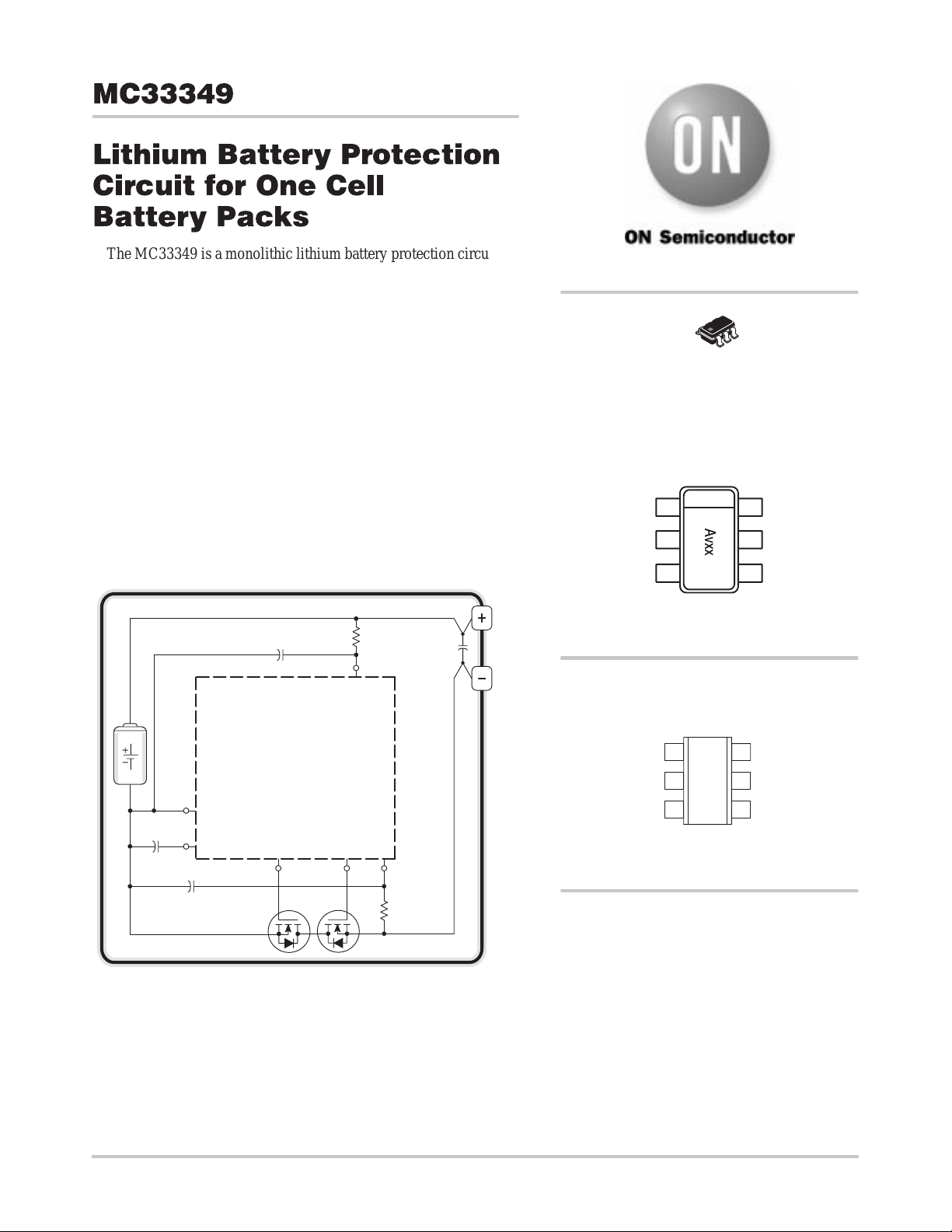
The MC33349 is a monolithic lithium battery protection circuit that
is designed to enhance the useful operating life of a one cell
rechargeable battery pack. Cell protection features consist of
internally trimmed charge and discharge voltage limits, discharge
current limit detection, and a low current standby mode when the cell
is discharged. This protection circuit requires a minimum number of
external components and is targeted for inclusion within the battery
pack.
• Internally Trimmed Charge and Discharge Voltage Limits
• Discharge Current Limit Detection
• Low Current Standby Mode when Cells are Discharged
• Dedicated for One Cell Applications
• Minimum Components for Inclusion within the Battery Pack
• Available in a Low Profile Surface Mount Package
http://onsemi.com
6
1
PLASTIC PACKAGE
N SUFFIX
CASE 1262
(SOT–23)
MARKING DIAGRAMS
1
T ypical One Cell Smart Battery Pack
5
MC33349
6
4
132
v = Version code number
xx = Date code
PIN CONNECTIONS
16
DO
2
P–
CO
3
(Top View)
ORDERING INFORMATION
See detailed ordering and shipping information in the package
dimensions section on page 10 of this data sheet.
Gnd
5
V
cell
C
4
t
Semiconductor Components Industries, LLC, 2000
May, 2000 – Rev. 1
1 Publication Order Number:
MC33349/D
Page 2
MC33349
Á
Á
Á
Á
MAXIMUM RATINGS
Characteristics Symbol Value Unit
Supply Voltage (Pin 5 to Pin 6)
Input Voltage
P– Pin Voltage (Pin 5 to Pin 2) V
Ct Pin (Pin 4 to Pin 6) V
Output Voltage
CO Pin Voltage (Pin 3 to Pin 2) V
DO Pin Voltage (Pin 1 to Pin 6) V
Power Dissipation
Operating Junction Temperature
Storage Temperature
БББББББББББББББ
ÁÁÁÁ
V
DD
P–
Ct
CO
DO
P
D
T
J
T
stg
БББББББ
–0.3 to 12
VDD – 28 to VDD + 0.3 V
Gnd – 0.3 to VDD + 0.3 V
VDD – 28 to VDD + 0.3 V
Gnd – 0.3 to VDD + 0.3 V
150
mW
–40 to 85
–55 to 125
ÁÁ
V
°C
°C
ELECTRICAL CHARACTERISTICS (C
= 0.01 µF, TA = 25°C, for min/max values TA is the operating junction temperature range
t
that applies, unless otherwise noted.)
Characteristic
Symbol Min Typ Max Unit Note
VOLTAGE SENSING
Cell Charging Cutoff (Pin 5 to Pin 6)
Overvoltage Threshold, VDD Increasing V
DET1
–3, –4 Suffix 4.2 4.25 4.3 V
–7 Suffix 4.3 4.35 4.4 V
Overvoltage Hysteresis VDD Decreasing V
HYS1
150 200 250 mV B
Cell Discharging Cutoff (Pin 5 to Pin 6)
Undervoltage Threshold, VDD Decreasing V
Overvoltage Delay Time (Ct = 0.01 µF, VDD = 3.6V to 4.5V) t
Undervoltage Delay Time (VDD = 3.6V to 2.4V) t
DET2
(DET1)
(DET2)
2.437 2.5 2.563 V
55 80 105 ms B
7.0 10 13 ms C
CURRENT SENSING
Excess Current Threshold (Detect rising edge of P– pin voltage)
V
DET3
–3, –7 Suffix 170 200 230 mV
–4 Suffix 45 75 105 mV
Short Protection Voltage (VDD = 3.0V)
V
SHORTVDD
– 1.1
VDD – 0.8
VDD – 0.5
V
Current Limit Delay Time (VDD = 3.0V)
Reset Resistance for Short Protection
t
(DET3)
t
(SHORT)
R
SHORT
9.0 13 17 ms D
– 5.0 50 µs D
50
100
150
k
W
OUTPUTS
CO Nch On Voltage (IO = 50 µA, VDD = 4.4V)
CO Pch On Voltage (IO = –50 µA, VDD = 3.9V)
DO Nch On Voltage (IO = 50 µA, VDD = 2.4V)
DO Pch On Voltage (IO = –50 µA, VDD = 3.9V)
V
V
V
V
ol1
oh1
ol2
oh2
3.4
3.4
–
–
0.2
3.8
0.2
3.7
0.5
0.5
V
–
V
V
–
V
TOTAL DEVICE
Operating Input Voltage
Supply Current
V
DD
I
cell
1.5
–
10
V
Operating (VDD = 3.9 V, VP– = 0V) – 3.0 6.0 µA I
Standby (VDD = 2.0 V) – 0.3 0.6 µA I
Minimum Operating Cell Voltage for Zero Volt Charging (Pin 5 to
Pin 2)
1. Indicates test circuits shown on next page.
V
ST
–
–
1.2
V
1
B
C
D
D
D
E
F
G
H
A
A
http://onsemi.com
2
Page 3
MC33349
A
B
C
F
A
5
V
V
2
6
3
1
OSCILLOSCOPE
5
2
6
3
V
G
5
4
V
2
3
6
5
2
6
1
A
V
H
A
5
5
1
D
E
V
2
6
1
2
6
V
I
5
A
2
A
V
6
5
2
6
1
3
A
V
5
2
6
Figure 1. T est Circuit Schematics
http://onsemi.com
3
Page 4
Vcell Ct
Á
Á
Á
Á
Á
Á
Á
Á
Á
5 4
VD1
VD2
VD3
MC33349
Level
Shift
Delay
10 kOhm
Short Circuit
Detector
Gnd Do Co P–
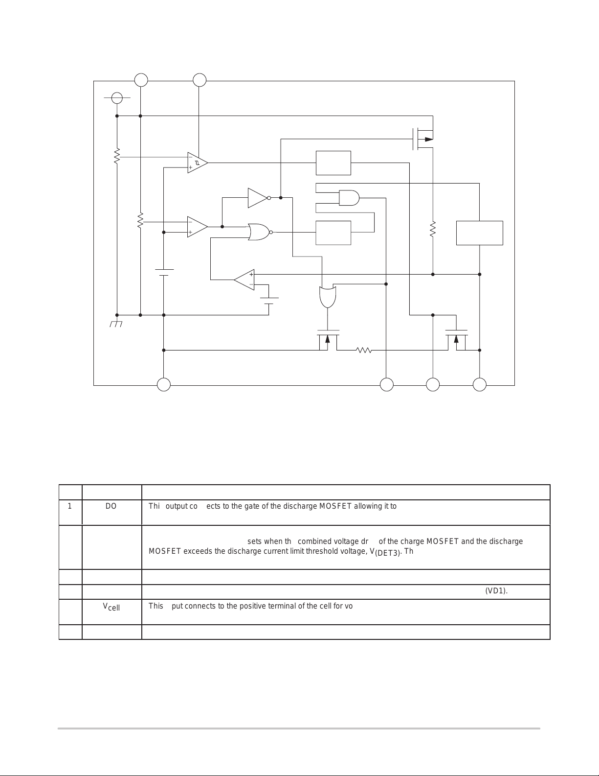
Figure 2. Detailed Block Diagram
PIN FUNCTION DESCRIPTION
Pin Symbol Description
1
2
Á
Á
3
4
5
Á
6
DO
P–
ÁÁÁ
ÁÁÁ
CO
C
t
V
cell
ÁÁÁ
Gnd
This output connects to the gate of the discharge MOSFET allowing it to enable or disable battery pack
discharging.
This pin monitors cell discharge current.
ББББББББББББББББББББББББББ
The excess current detector sets when the combined voltage drop of the charge MOSFET and the discharge
MOSFET exceeds the discharge current limit threshold voltage, V
ББББББББББББББББББББББББББ
V
is pulled within 0.8V of the cell voltage by a short circuit.
(P–)
This output connects to the gate of the charge MOSFET allowing it to enable or disable battery pack charging.
This pin connects to the external capacitor for setting the output delay of the overvoltage detector (VD1).
This input connects to the positive terminal of the cell for voltage monitoring and provides operating bias for the
ББББББББББББББББББББББББББ
integrated circuit.
This is the ground pin of the IC.
Rshort
1 3 26
. The short circuit detector activates when
(DET3)
http://onsemi.com
4
Page 5

O
ER
OLTAGE
T
RES
OLD
(
)
4.27
E
CESS
C
RRE
T
T
RES
OLD
(
)
O
TP
T
DELAY
O
O
ER
OLTAGE
2.54
V
4.26
DET1
V
4.25
H
4.24
H
4.23
4.22
V
4.21
V
4.20
0.210
V
DET3
V
0.205
H
TYPICAL CHARACTERISTICS
–40 –20 0 20 40 60 80 100
–60
TA, AMBIENT TEMPERATURE (°C)
Figure 3. Overvoltage Threshold
vs T emperature
MC33349N–3X
MC33349
2.53
DET2
2.52
2.51
2.50
2.49
2.48
UNDERVOLTAGE THRESHOLD V (V)
2.47
–40 –20 0 20 40 60 80 100
–60
Figure 4. Undervoltage Threshold
MC33349N–3X / MC33349N–7X
2.40
VDD = 3.0 V
short
2.35
2.30
TA, AMBIENT TEMPERATURE (°C)
vs T emperature
H
0.200
N
U
0.195
X
0.190
–60
100
90
80
V
V
70
F
60
VDET1
t (ms)
50
40
U
U
30
20
–60
–40 –20 0 20 40 60 80 100
TA, AMBIENT TEMPERATURE (°C)
Figure 5. Excess Current Threshold
vs T emperature
MC33349N–3X / MC33349N–7X
C3 = 0.01µF
VDD = 3.6V to 4.3V
–40 –20 0 20 40 60 80 100
TA, AMBIENT TEMPERATURE (°C)
Figure 7. Output Delay of Overvoltage
vs T emperature
MC33349N–3X
2.25
2.20
2.15
SHORT PROTECTION VOLTAGE V (V)
2.10
–60
18
16
14
12
10
VDET2
t (ms)
8
6
4
OUTPUT DELAY OF UNDERVOLTAGE
2
–60
–40 –20 0 20 40 60 80 100
TA, AMBIENT TEMPERATURE (°C)
Figure 6. Short Protection Voltage
vs T emperature
MC33349N–3X
VDD = 3.6V to 2.4V
–40 –20 0 20 40 60 80 100
TA, AMBIENT TEMPERATURE (°C)
Figure 8. Output Delay of Undervoltage
vs T emperature
MC33349N–3X / MC33349N–7X
http://onsemi.com
5
Page 6

MC33349
O
ER–C
ARGE
T
RES
OLD
YSTERESIS
(
)
O
TP
T
DELAY
O
E
CESS
C
RRE
T
STA
D
Y
C
RRE
T
Icell
(
A)
20
N
18
16
U
14
12
X
10
F
VDET3
8
t (ms)
6
U
4
U
2
0
mV
0.210
HYS1
V
0.205
H
0.200
H
H
0.195
H
0.190
–60
V
VDD = 3.0 V
–40 –20 0 20 40 60 80 100
–60
TA, AMBIENT TEMPERATURE (°C)
Figure 9. Output Delay of Excess Current
vs T emperature
MC33349N–3X
–40 –20 0 20 40 60 80 100
TA, AMBIENT TEMPERATURE (°C)
10
8
6
4
DETECTOR tshort ( s)µ
2
OUTPUT DELAY OF SHORT CIRCUIT
0
–60
4.0
3.5
3.0
2.5
2.0
1.5
1.0
OPERATING CURRENT Icell ( A)µ
0.5
0.0
–60
VDD = 3.0 V
–40 –20 0 20 40 60 80 100
TA, AMBIENT TEMPERATURE (°C)
Figure 10. Output Delay of Short Circuit
Detector vs T emperature
MC33349N–3X
VDD = 3.9 V
VP– = 0 V
–40 –20 0 20 40 60 80 100
TA, AMBIENT TEMPERATURE (°C)
Figure 11. Overvoltage Threshold Hysteresis
vs T emperature
MC33349N–3X / MC33349N–7X
0.40
0.35
µ
0.30
N
0.25
0.20
U
0.15
B
N
0.10
0.05
0.00
–40 –20 0 20 40 60 80 100
–60
TA, AMBIENT TEMPERATURE (°C)
Figure 13. Standby Current vs T emperature
MC33349N–3X
VDD = 2.0 V
0.30
OL1
0.25
0.20
0.15
0.10
0.05
Cout Nch DRIVER ON VOLTAGE V (V)
0.00
–60
Figure 14. Cout Nch Driver On Voltage (Vol1)
Figure 12. Operating Current
vs T emperature
MC33349N–3X
IOL = 50µA
VDD = 4.4V
–40 –20 0 20 40 60 80 100
TA, AMBIENT TEMPERATURE (°C)
vs T emperature
MC33349N–3X
http://onsemi.com
6
Page 7

MC33349
3.9
Co
t
Pch
DRI
ER
O
OLTAGE
(
)
.3
Do
t
Pch
DRI
ER
O
OLTAGE
(
)
0
V
OH1
3.85
V
3.80
N V
3.75
V
3.70
3.65
u
3.60
–40 –20 0 20 40 60 80 100
–60
TA, AMBIENT TEMPERATURE (°C)
Figure 15. Cout Pch Driver On Voltage (Voh1)
vs T emperature
MC33349N–3X
3.90
V
OH2
3.85
V
3.80
N V
3.75
V
3.70
3.65
u
3.60
–40 –20 0 20 40 60 80 100
–60
TA, AMBIENT TEMPERATURE (°C)
Figure 17. Dout Pch Driver On Voltage (Voh2)
vs T emperature
MC33349N–3X
IOH = –50µA
VDD = 3.9V
IOH = –50µA
VDD = 3.9V
0
0
OL2
0.25
0.20
0.15
0.10
0.05
Dout Nch DRIVER ON VOLTAGE V (V)
0.00
–60
10000
1000
µ
100
short
t ( s)
10
OUTPUT DELAY OF SHORT PROTECTION
0
0.001
IOL = 50µA
VDD = 2.4V
–40 –20 0 20 40 60 80 100
TA, AMBIENT TEMPERATURE (°C)
Figure 16. Dout Nch Driver On Voltage (Vol2)
vs T emperature
MC33349N–3X
R2 = 1k
W
VDD = 3.0V
0.01 1
EXTERNAL CAPACITANCE C2 (µF)
0.1
Figure 18. Short Protection Delay Time
vs Capacitance C2
MC33349N–3X
25.00
20.00
15.00
VDET3
t (ms)
10.00
5.00
OUTPUT DELAY OF EXCESS CURRENT
0.00
2.5
Figure 19. Excess Current Delay Time vs V
3.0 3.5 4.0 4.5
SUPPLY VOLTAGE VDD (V)
DD
MC33349N–3X
http://onsemi.com
7
Page 8

4.258
.21
E
CESS
C
RRE
T
T
RES
OLD
(
V
)
0
0.209
DET3
V
0.208
H
0.207
H
0.206
N
0.205
U
0.204
0.203
X
0.202
0
0
0.5 1 1.5 2 2.5 3
EXTERNAL RESISTANCE R2(kW)
Figure 20. Excess Current Threshold vs
External Resistance R2
MC33349N–3X / MC33349N–7X
MC33349
C1 = 0 to 0.68µF
4.256
DET1
4.254
4.252
4.250
VDD = 3.0V
OPERATING DESCRIPTION
4.248
OVERVOLTAGE THRESHOLD V (V)
4.246
0 200 400 600 800 1000
Figure 21. Overvoltage Threshold vs
C3 = 0.22µF
C3 = 0.1µF
C3 = 0.01µF
EXTERNAL RESISTANCE R1(W)
External Resistance R1
MC33349N–3X
VD1 / Over–Charge Detector
VD1 monitors the voltage at the V
it exceeds the over–charge detector threshold, V
pin (VDD). When
CELL
DET1
. VD1
senses an over–charging condition, the CO pin goes to a
”Low” level, and the external charge control,
Nch–MOSFET turns off.
Resetting VD1 allows resumption of the charging
process. VD1 resets under two conditions, thus, making the
CO pin level ”High.” The first case occurs when the cell
voltage drops below ”V
DET1
– V
HYS1
.” (V
HYS1
is typically
200 mV). In the second case, disconnecting the charger from
the battery pack can reset VD1 after VDD drops between
”V
DET1
” and ”V
DET1
– V
HYS1
”.
After detecting over–charge, connecting a load to the
battery pack allows load current to flow through the parasitic
diode of the external charge control FET . The CO level goes
”High” when the cell voltage drops below V
DET1
due to load
current draw through the parasitic diode.
An external capacitor connected between the Gnd pin and
Ct pin sets the output delay time for over–charge detection.
The external capacitor sets up a delay time from the moment
of over–charge detection to the time CO outputs a signal,
which enables the charge control FET to turn off. If the
voltage fault occurs within the time delay window . CO will
not turn off the charge control FET. The output delay time
can be calculated as follows:
*
t
VDET1
[sec]+(Ct[F] (VDD[V]*0.7)ń(0.48 10
6
A level shifter incorporated in a buffer driver for the CO
pin drives the ”Low” level of CO pin to the P– pin voltage.
A CMOS buffer sets the ”High” level of CO pin to VDD.
VD2 / Over–Discharge Detector
VD2 monitors the voltage at the V
CELL
pin (V
DD)
. When
it drops below the over–discharge detector threshold,
V
, VD2 senses an over–discharge condition, the DO
DET2
pin goes to a ”Low” level, and the external discharge control
Nch MOSFET turns off. The IC enters a low current standby
mode after detection of an over–discharged voltage by VD2.
Supply current then reduces to approximately 0.3 µA.
During standby mode, only the charger detector operates.
VD2 can only reset after connecting the pack to a charger .
While VDD remains under the over–discharge detector
threshold, V
, discharge current can flow through the
DET2
parasitic diode of the external discharge control FET. The
DO level goes ”High” when the cell voltage rises above
V
due to the charging current through the parasitic
DET2
diode. Connecting a charger to the battery pack will instantly
set DO ”High” if this causes VDD to rise above V
DET2
.
When cell voltage equals zero, one can charge the battery
pack if the voltage is greater than the minimum charge
voltage, VST.
Output delay time for the over–discharge detection
(t
VDET2
) is fixed internally. If the voltage fault occurs within
the time delay window, DO will not turn off the discharge
control FET.
A CMOS buffer sets the output of the DO pin to a ”High”
level of VDD and a ”Low” level of Gnd.
VD3 / Excess Current Detector, Short Circuit Detector
Both the excess current detector and the short circuit
detector can work when the two control FET’s are on. When
the voltage at the P– pin rises to a value between the short
)
circuit protection voltage, V
threshold, V
Increasing V
, the excess current detector operates.
DET3
higher than V
(P–)
SHORT
SHORT
, and the excess current
enables the short
circuit detector. The DO pin then goes to a ”Low” level, and
the external discharge control Nch MOSFET turns off.
Output delay time for excess current detection (t
VDET3
) is
fixed internally. If the excess current fault occurs within the
time delay window, DO will not turn off the discharge
control FET. However, when the short circuit protector is
http://onsemi.com
8
Page 9

MC33349
enabled, DO can turn off the discharge control FET . Its delay
time would be approximately 5 µs.
The P– pin has a built–in pull down resistor, typically 100
kW, which connects to the Gnd pin. Once an excess current
or short circuit fault is removed, the internal resistor pulls
V
to the Gnd pin potential. Therefore, the voltage from
(P–)
P– to Gnd drops below the current detection thresholds and
DO turns the external MOSFET back on.
–NOTE–
If VDD voltage is higher than the over–discharge voltage
threshold, V
, when excess current is detected the IC
DET2
will not enter a standby mode. However, if VDD is below
V
when excess current is detected, the IC will enter a
DET2
standby mode. This will not occur when the short circuit
detector activates.
Figure 22. Timing Diagram / Operational Description
http://onsemi.com
9
Page 10

C1
0.01µF
R1
100
MC33349
+
W
5
4
C3
0.01µF
6
0.22µF
C2
MC33349
1
2
3
R2
1k
W
–
Figure 23. T ypical Application Circuit
Technical Notes
R1 and C1 will stabilize a supply voltage to the MC33349. A recommended R1 value is less than 1 kW. A larger value of R1
leads to higher detection voltage because of shoot through current into the IC.
R2 and C2 stabilize P– pin voltage. Larger R2 values could possibly disable reset from over–discharge by connecting a charger .
Recommended values are less than 1 kW. After an over–charge detection even connecting a battery pack to a system could
probably not allow a system to draw load current if one uses a larger R2C2 time constant. The recommended C2 value is less
than 1µF.
R1 and R2 can operate as a current limiter against setting cell reverse direction or for applying excess charging voltage to the
IC and battery pack. Smaller R1 and R2 values may cause excessive power consumption over the specified power dissipation
rating. Therefore R1+R2 should be more than 1 kW.
The time constants R1C1 and R2C2 must have a relation as follows:
R1C1 ≤ R2C2
If the R1C1 time constant for the Vcell pin is larger than the R2C2 time constant for the P– pin, the IC might enter a standby
mode after detecting excess current. This was noted in the operating description of the current detectors.
ORDERING INFORMATION
Overvoltage
Device
MC33349N–3R1 4.25 2.5 0.2 A1xx*
MC33349N–4R1 4.25 2.5 0.075 A2xx*
MC33349N–7R1 4.35 2.5 0.2 A0xx*
* ″xx″ denotes the date code marking.
Consult factory for information on other threshold values.
Threshold (V)
Undervoltage
Threshold (V)
Current Limit
Threshold (V)
Marking Reel Size Tape width Quantity
http://onsemi.com
10
7” 8 mm 3000
Page 11

PIN 1 INK MARK
IDENTIFIER
1
D
2
3
A
H
E1
MC33349
OUTLINE DIMENSIONS
N SUFFIX
PLASTIC PACKAGE
CASE 1262–01
(SOT–23)
ISSUE O
E
M
0.20 CMB
6
A
e
5
e1
A
4
A1
B
q
A
c1
L
b1
0.05
NOTES:
1. DIMENSIONS ARE IN MILLIMETERS.
C
S
B
S
A
b
M
0.10 C
b
c
2. INTERPRET DIMENSIONS AND TOLERANCES
PER ASME Y14.5M, 1994.
3. DIMENSION D DOES NOT INCLUDE FLASH OR
PROTRUSIONS. FLASH OR PROTRUSIONS
SHALL NOT EXCEED 0.23 PER SIDE.
4. TERMINAL NUMBERS ARE SHOWN FOR
REFERENCE ONLY.
5. DIMENSIONS D AND E1 ARE TO BE DETERMINED
AT DATUM PLANE H.
MILLIMETERS
DIM MIN MAX
A 0.90 1.45
A1 0.00 0.15
b 0.35 0.50
b1 0.35 0.45
c 0.09 0.20
c1 0.09 0.15
D 2.80 3.00
E 2.60 3.00
E1 1.50 1.75
0.95
e
1.90
e1
L 0.25 0.55
q
0 10
__
SECTION A–A
http://onsemi.com
11
Page 12

MC33349
ON Semiconductor and are trademarks of Semiconductor Components Industries, LLC (SCILLC). SCILLC reserves the right to make changes
without further notice to any products herein. SCILLC makes no warranty , representation or guarantee regarding the suitability of its products for any particular
purpose, nor does SCILLC assume any liability arising out of the application or use of any product or circuit, and specifically disclaims any and all liability ,
including without limitation special, consequential or incidental damages. “Typical” parameters which may be provided in SCILLC data sheets and/or
specifications can and do vary in different applications and actual performance may vary over time. All operating parameters, including “Typicals” must be
validated for each customer application by customer’s technical experts. SCILLC does not convey any license under its patent rights nor the rights of others.
SCILLC products are not designed, intended, or authorized for use as components in systems intended for surgical implant into the body, or other applications
intended to support or sustain life, or for any other application in which the failure of the SCILLC product could create a situation where personal injury or
death may occur. Should Buyer purchase or use SCILLC products for any such unintended or unauthorized application, Buyer shall indemnify and hold
SCILLC and its officers, employees, subsidiaries, affiliates, and distributors harmless against all claims, costs, damages, and expenses, and reasonable
attorney fees arising out of, directly or indirectly , any claim of personal injury or death associated with such unintended or unauthorized use, even if such claim
alleges that SCILLC was negligent regarding the design or manufacture of the part. SCILLC is an Equal Opportunity/Affirmative Action Employer .
PUBLICATION ORDERING INFORMATION
NORTH AMERICA Literature Fulfillment:
Literature Distribution Center for ON Semiconductor
P.O. Box 5163, Denver, Colorado 80217 USA
Phone: 303–675–2175 or 800–344–3860 Toll Free USA/Canada
Fax: 303–675–2176 or 800–344–3867 Toll Free USA/Canada
Email: ONlit@hibbertco.com
Fax Response Line: 303–675–2167 or 800–344–3810 T oll Free USA/Canada
N. American Technical Support: 800–282–9855 Toll Free USA/Canada
EUROPE: LDC for ON Semiconductor – European Support
German Phone: (+1) 303–308–7140 (M–F 1:00pm to 5:00pm Munich Time)
Email: ONlit–german@hibbertco.com
French Phone: (+1) 303–308–7141 (M–F 1:00pm to 5:00pm Toulouse T ime)
Email: ONlit–french@hibbertco.com
English Phone: (+1) 303–308–7142 (M–F 12:00pm to 5:00pm UK Time)
Email: ONlit@hibbertco.com
EUROPEAN TOLL–FREE ACCESS*: 00–800–4422–3781
*Available from Germany, France, Italy, England, Ireland
CENTRAL/SOUTH AMERICA:
Spanish Phone: 303–308–7143 (Mon–Fri 8:00am to 5:00pm MST)
Email: ONlit–spanish@hibbertco.com
ASIA/PACIFIC : LDC for ON Semiconductor – Asia Support
Phone: 303–675–2121 (Tue–Fri 9:00am to 1:00pm, Hong Kong Time)
T oll Free from Hong Kong & Singapore:
001–800–4422–3781
Email: ONlit–asia@hibbertco.com
JAPAN: ON Semiconductor, Japan Customer Focus Center
4–32–1 Nishi–Gotanda, Shinagawa–ku, T okyo, Japan 141–0031
Phone: 81–3–5740–2745
Email: r14525@onsemi.com
ON Semiconductor Website: http://onsemi.com
For additional information, please contact your local
Sales Representative.
http://onsemi.com
12
MC33349/D
 Loading...