

Page 1
The MC33341 is a monolithic regulation control circuit that is specifically
designed to close the voltage and current feedback loops in power supply
and battery charger applications. This device features the unique ability to
perform source high–side, load high–side, source low–side and load
low–side current sensing, each with either an internally fixed or externally
adjustable threshold. The various current sensing modes are accomplished
by a means of selectively using the internal differential amplifier, inverting
amplifier, or a direct input path. Positive voltage sensing is performed by an
internal voltage amplifier. The voltage amplifier threshold is internally fixed
and can be externally adjusted in all low–side current sensing applications.
An active high drive output is provided to directly interface with economical
optoisolators for isolated output power systems. This device is available in
8–lead dual–in–line and surface mount packages.
• Differential Amplifier for High–Side Source and Load Current Sensing
• Inverting Amplifier for Source Return Low–Side Current Sensing
• Non–Inverting Input Path for Load Low–Side Current Sensing
• Fixed or Adjustable Current Threshold in All Current Sensing Modes
• Positive Voltage Sensing in All Current Sensing Modes
• Fixed Voltage Threshold in All Current Sensing Modes
• Adjustable Voltage Threshold in All Low–Side Current Sensing Modes
• Output Driver Directly Interfaces with Economical Optoisolators
• Operating Voltage Range of 2.3 V to 16 V
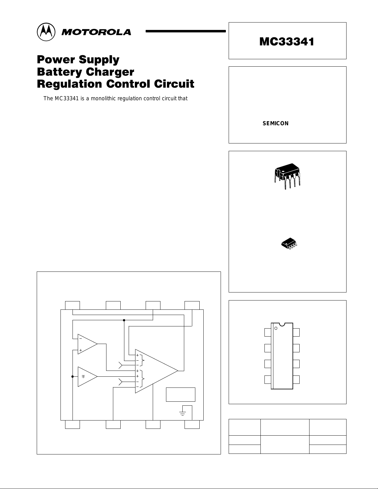
Representative Block Diagram
Drive
Output
8
V
CC
7
Current Sense Input B/
Voltage Threshold Adjust
6
Voltage Sense
Input
5
Order this document by MC33341/D
POWER SUPPLY
BATTERY CHARGER
REGULATION
CONTROL CIRCUIT
SEMICONDUCTOR
TECHNICAL DATA
8
1
P SUFFIX
PLASTIC PACKAGE
CASE 626
8
1
D SUFFIX
PLASTIC PACKAGE
CASE 751
(SO–8)
PIN CONNECTIONS
Differential
Amp
1.0
1.2 V
#
1.0
Inverting/
Noninverting Amp
1
Current Sense
Input A
This device contains 114 active transistors.
0.2 V
2
Current
Threshold Adjust
MOTOROLA ANALOG IC DEVICE DATA
Voltage and Current
Transconductance
Amp/Driver
V
I
Reference
3
Compensation
4
Gnd
Current Sense
Input A
Current Threshold
Adjust
Compensation
Gnd
18
2
3
4
(Top View)
Drive Output
V
7
CC
Current Sense Input B/
6
Voltage Threshold Adjust
Voltage Sense Input
5
ORDERING INFORMATION
Operating
Device
MC33341D
MC33341P
Motorola, Inc. 1998 Rev 1
Temperature Range
TA = –25° to +85°C
Package
SO–8
Plastic DIP
1
Page 2
MAXIMUM RATINGS
Á
Á
Á
Á
Á
Á
Á
Á
Á
Á
ÁÁÁÁ
ÁÁÁÁ
ÁÁÁÁ
ÁÁÁÁ
ÁÁÁÁ
ÁÁÁÁ
ÁÁÁÁ
Rating Symbol Value Unit
Power Supply Voltage (Pin 7)
Voltage Range
Current Sense Input A (Pin 1)
ББББББББББББББ
Current Threshold Adjust (Pin 2)
ББББББББББББББ
Compensation (Pin 3)
Voltage Sense Input (Pin 5)
ББББББББББББББ
Current Sense Input B/Voltage Threshold Adjust (Pin 6)
ББББББББББББББ
Drive Output (Pin 8)
Drive Output Source Current (Pin 8) I
Thermal Resistance, Junction–to–Air
P Suffix, DIP Plastic Package, Case 626
ББББББББББББББ
D Suffix, SO–8 Plastic Package, Case 751
Operating Junction Temperature (Note 1)
Storage Temperature
NOTE: ESD data available upon request.
MC33341
V
CC
V
IR
ÁÁ
ÁÁ
ÁÁ
ÁÁ
Source
R
θJA
ÁÁ
T
J
T
stg
16
–1.0 to V
CC
ÁÁÁ
ÁÁÁ
ÁÁÁ
ÁÁÁ
50 mA
100
ÁÁÁ
178
–25 to +150
–55 to +150
V
V
Á
Á
Á
Á
°C/W
Á
°C
°C
ELECTRICAL CHARACTERISTICS (V
= 6.0 V, TA = 25°C, for min/max values TA is the operating junction
CC
temperature range that applies (Note 1), unless otherwise noted.)
Characteristic
Symbol Min Typ Max Unit
CURRENT SENSING (Pins 1, 2, 6)
High–Side Source and Load Sensing Pin 1 to Pin 6 (Pin 1 >1.6 V)
V
th(I HS)
Internally Fixed Threshold Voltage (Pin 2 = VCC)
TA = 25°C 187 197 207
TA = T
low
to T
high
183 – 211
Externally Adjusted Threshold Voltage (Pin 2 = 0 V) – 10 –
Externally Adjusted Threshold Voltage (Pin 2 = 200 mV) – 180 –
Low–Side Load Sensing Pin 1 to Pin 4 (Pin 1 = 0 V to 0.8 V)
V
th(I LS+)
Internally Fixed Threshold Voltage (Pin 2 = VCC)
TA = 25°C 194 200 206
TA = T
low
to T
high
192 – 208
Externally Adjusted Threshold Voltage (Pin 2 = 0 V) – 10 –
Externally Adjusted Threshold Voltage (Pin 2 = 200 mV) – 180 –
Low–Side Source Return Sensing Pin 1 to 4 (Pin 1 = 0 V to –0.2 V)
V
th(I LS–)
Internally Fixed Threshold Voltage (Pin 2 = VCC)
TA = 25°C –195 –201 –207
TA = T
low
to T
high
–193 – –209
Externally Adjusted Threshold Voltage (Pin 2 = 0 V) – –10 –
Externally Adjusted Threshold Voltage (Pin 2 = 200 mV) – –180 –
Current Sense Input A (Pin 1)
Input Bias Current, High–Side Source and Load Sensing
(Pin 2 = 0 V to V
Pin 6
V)
Input Bias Current, Low–Side Load Sensing
(Pin 2 = 0 V to 0.8 V)
Input Resistance, Low–Side Source Return Sensing
(Pin 2 = –0.6 V to 0 V)
Current Sense Input B/Voltage Threshold Adjust (Pin 6)
I
IB(A HS)
I
IB(A LS+)
R
in(A LS–)
I
IB(B)
– 40 – µA
– 10 – nA
– 10 – kΩ
Input Bias Current
High–Side Source and Load Current Sensing (Pin 6 > 2.0 V) – 20 – µA
Voltage Threshold Adjust (Pin 6 < 1.2 V) – 100 – nA
Current Sense Threshold Adjust (Pin 2)
I
IB(I th)
–
10
–
Input Bias Current
Transconductance, Current Sensing Inputs to Drive Output
NOTE: 1. T ested ambient temperature range for the MC33341: T
= –25°C, T
low
high
g
m(I)
= +85°C.
–
6.0
–
mV
mV
mV
nA
mhos
2
MOTOROLA ANALOG IC DEVICE DATA
Page 3
MC33341
ÁÁÁÁ
ÁÁÁÁ
ÁÁÁÁ
ÁÁÁÁ
ÁÁÁÁ
ÁÁÁÁ
ÁÁÁÁ
Á
Á
Á
Á
Á
Á
Á
Á
Á
Á
Á
Á
Á
Á
Á
Á
Á
Á
Á
Á
Á
Á
Á
Á
Á
Á
Á
Á
Á
Á
Á
Á
Á
Á
Á
Á
Á
Á
Á
ELECTRICAL CHARACTERISTICS (continued) (V
= 6.0 V, TA = 25°C, for min/max values TA is the operating junction
CC
temperature range that applies (Note 1), unless otherwise noted.)
Characteristic UnitMaxTypMinSymbol
DIFFERENTIAL AMPLIFIER DISABLE LOGIC (Pins 1, 6)
Logic Threshold Voltage Pin 1 (Pin 6 = 0 V)
Enabled, High–Side Source and Load Current Sensing V
Disabled, Low–Side Load and Source Return Current Sensing V
th(I HS)
th(I LS)
– ≥1.7 –
– ≤1.3 –
VOLTAGE SENSING (Pins 5, 6)
Positive Sensing Pin 5 to Pin 4
V
th(V)
Internally Fixed Threshold Voltage
TA = 25°C 1.186 1.210 1.234 V
TA = T
low
to T
high
1.174 – 1.246 V
Externally Adjusted Threshold Voltage (Pin 6 = 0 V) – 40 – mV
Externally Adjusted Threshold Voltage (Pin 6 = 1.2 V) – 1.175 – V
Voltage Sense, Input Bias Current (Pin 5)
Transconductance, Voltage Sensing Inputs to Drive Output
I
IB(V)
g
m(V)
–
–
10
7.0
–
–
DRIVE OUTPUT (Pin 8)
High State Source Voltage (I
High State Source Current (Pin 8 = 0 V)
Source
= 10 mA)
V
OH
I
Source
15
–
VCC – 0.8
20
–
–
TOTAL DEVICE (Pin 7)
Operating Voltage Range
Power Supply Current (VCC = 6.0 V)
NOTE: 1. T ested ambient temperature range for the MC33341: T
= –25°C, T
low
high
V
CC
I
CC
= +85°C.
2.5 to 15
–
2.3 to 15
300
–
600
V
nA
mhos
V
mA
V
µA
PIN FUNCTION DESCRIPTION
Pin Name Description
1
Current Sense Input A
Á
Á
Á
Á
Á
Á
Á
Á
Á
Á
Á
Á
Á
ББББББ
ББББББ
ББББББ
ББББББ
2
Current Threshold Adjust
ББББББ
3
Compensation
ББББББ
4
Ground
5
Voltage Sense Input
ББББББ
6
Current Sense Input B/
ББББББ
Voltage Threshold Adjust
ББББББ
ББББББ
ББББББ
7
V
CC
8
Drive Output
ББББББ
ББББББ
This multi–mode current sensing input can be used for either source high–side, load high–side,
source–return low–side, or load low–side sensing. It is common to a Differential Amplifier, Inverting
БББББББББББББББББББББББ
Amplifier, and a Noninverting input path. Each of these sensing paths indirectly connect to the current
БББББББББББББББББББББББ
sense input of the Transconductance Amplifier. This input is connected to the high potential side of a
current sense resistor when used in source high–side, load high–side, or load low–side current
БББББББББББББББББББББББ
sensing modes. In source return low–side current sensing mode, this pin connects to the low potential
БББББББББББББББББББББББ
side of a current sense resistor.
The current sense threshold can be externally adjusted over a range of 0 V to 200 mV with respect to
Pin 4, or internally fixed at 200 mV by connecting Pin 2 to VCC.
БББББББББББББББББББББББ
This pin is connected to a high impedance node within the transconductance amplifier and is made
available for loop compensation. It can also be used as an input to directly control the Drive Output.
БББББББББББББББББББББББ
An active low at this pin will force the Drive Output into a high state.
This pin is the regulation control IC ground. The control threshold voltages are with respect to this pin.
This is the voltage sensing input of the Transconductance Amplifier. It is normally connected to the
power supply/battery charger output through a resistor divider. The input threshold is controlled by
БББББББББББББББББББББББ
Pin 6.
This is a dual function input that is used for either high–side current sensing, or as a voltage threshold
БББББББББББББББББББББББ
adjustment for Pin 5. This input is connected to the low potential side of a current sense resistor when
used in source high–side or load high–side current sensing modes. In all low–side current sensing
БББББББББББББББББББББББ
modes, Pin 6 is available as a voltage threshold adjustment for Pin 5. The threshold can be externally
БББББББББББББББББББББББ
adjusted over a range of 0 V to 1.2 V with respect to Pin 4, or internally fixed at 1.2 V by connecting
Pin 6 to VCC.
БББББББББББББББББББББББ
This is the positive supply voltage for the regulation control IC. The typical operating voltage range is
2.3 V to 15 V with respect to Pin 4.
This is a source–only output that normally connects to a linear or switching regulator control circuit.
БББББББББББББББББББББББ
This output is capable of 15 mA, allowing it to directly drive an optoisolator in primary side control
applications where galvanic isolation is required.
БББББББББББББББББББББББ
MOTOROLA ANALOG IC DEVICE DATA
3
Page 4
MC33341
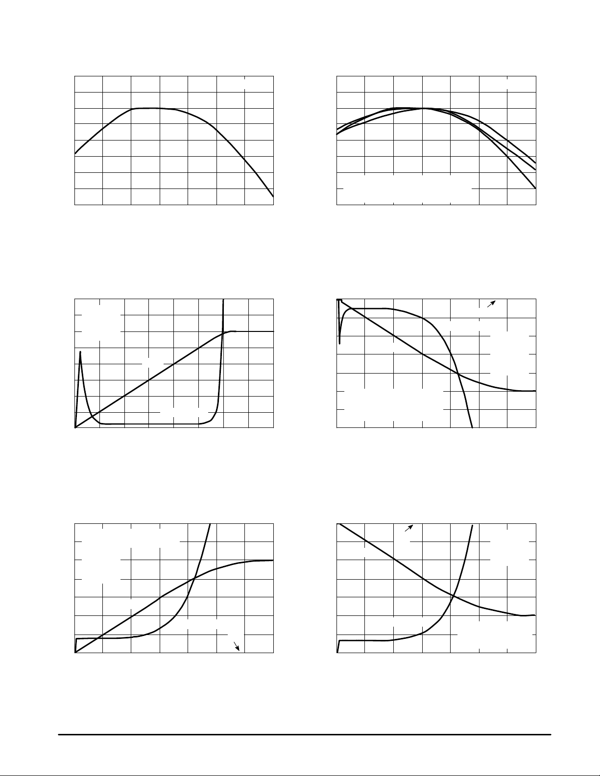
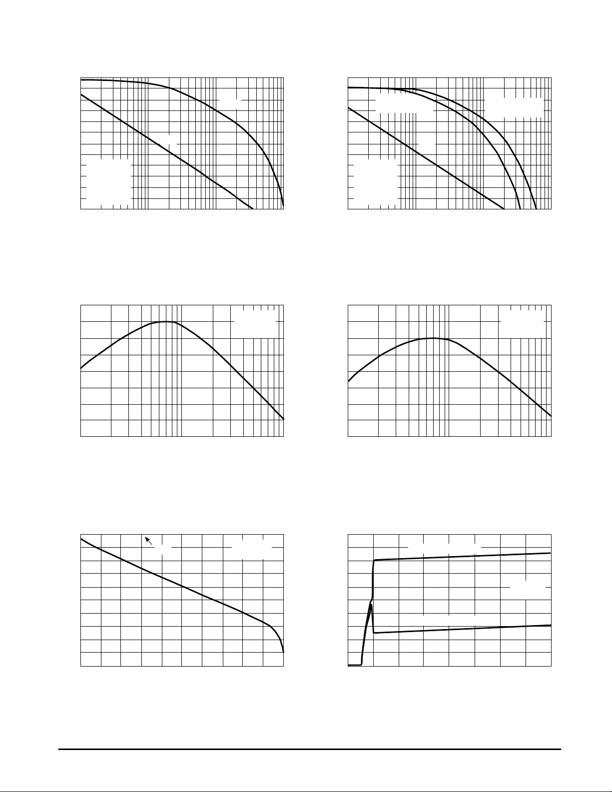
Figure 1. V oltage Sensing
Threshold Change versus T emperature
4.0
0
–4.0
–8.0
, VOLTAGE SENSING THRESHOLD CHANGE (mV)
–12
–50
th(v)
V
∆
–25 0 25 50 75 100 125
TA, AMBIENT TEMPERATURE (°C)
Figure 3. Closed–Loop V oltage Sensing Input
versus V oltage Threshold Adjust
1.6
VCC = 6.0 V
1.4
VO = 1.0 V
IO = 1.0 mA
, VOLTAGE SENSING INPUT (V)
Pin 5
V
1.2
1.0
0.8
0.6
0.4
0.2
0
0
°
C
TA = 25
V
Pin 5
V
Pin 6–VPin 5
0.2 0.4 0.6 0.8 1.0 1.2 1.4 1.6 40 80 120 160 200 240 280
V
, VOLTAGE THRESHOLD ADJUST (V)
Pin 6
VCC = 6.0 V
16
14
12
10
8.0
6.0
4.0
2.0
0
Threshold Change versus T emperature
1.0
0
–1.0
, CURRENT SENSING
–2.0
th(I HS)
THRESHOLD CHANGE (mV)
V
∆
1 – Source High–Side and Load High–Side
2 – Source Return Low–Side
3 – Load Low–Side
–3.0
–50
–25 0 25 50 75 100 125
Figure 4. Closed–Loop Current Sense Input B
0
–40
–80
–120
–160
–200
, INPUT DIFFERENCE VOL TAGE (mV)
, CURRENT SENSE INPUT B (mV)
Pin 5
V
–V
Pin 6
V
Differential Amplifier is active for
source high–side and load high–side
current sensing. Both vertical axis are
–240
Pin 6
expressed in millivolts down to VCC.
–280
0
Figure 2. Current Sensing
VCC = 6.0 V
TA, AMBIENT TEMPERATURE (
°
C)
versus Current Threshold Adjust
V
CC
V
Pin 1–VPin 6
V
Pin 6
V
, CURRENT THRESHOLD ADJUST (V)
Pin 2
VCC = 6.0 V
VO = 1.0 V
IO = 1.0 mA
Pin 1 = V
TA = 25
3
2
1
0
2.0
4.0
6.0
CC
°
C
8.0
10
, INPUT DIFFERENCE VOL TAGE (mV)
Pin 6
12
–V
14
Pin 1
V
Figure 5. Closed–Loop Current Sensing Input A
versus Current Threshold Adjust
280
Noninverting input path is active
240
for load low–side current sensing.
VCC = 6.0 V
200
VO = 1.0 V
IO = 1.0 mA
°
C
TA = 25
160
120
, CURRENT SENSE INPUT A (mV)
Pin 1
V
80
40
0
0
V
Pin 5
V
Pin 2–VPin 1
40 80 120 160 200 240 280 40 80 120 160 200 240 280
V
, CURRENT THRESHOLD ADJUST (mV)
Pin 2
4
Gnd
14
12
10
8.0
6.0
4.0
2.0
0
–120
–160
–200
, INPUT DIFFERENCE VOL TAGE (mV)
, CURRENT SENSE INPUT A (mV)
Pin 1
–240
Pin 1
–V
V
–260
Pin 2
V
Figure 6. Closed–Loop Current Sensing Input A
versus Current Threshold Adjust
0
–40
–80
Gnd
V
Pin 5
V
–|V
Pin 1
|
Inverting Amplifier is
active for source return
low–side current sensing.
Pin 2
0
V
, CURRENT THRESHOLD ADJUST (mV)
Pin 2
VCC = 6.0 V
VO = 1.0 V
IO = 1.0 mA
TA = 25
MOTOROLA ANALOG IC DEVICE DATA
14
12
10
°
C
8.0
6.0
4.0
|, INPUT DIFFERENCE VOL TAGE (mV)
Pin 1
2.0
–|V
0
Pin 2
V
Page 5
MC33341
Figure 7. Bode Plot
V oltage Sensing Inputs to Drive Output
60
50
40
30
VCC = 6.0 V
20
VOLTAGE GAIN (dB)
, VOLTAGE SENSING OPEN–LOOP
VOL(V)
A
VO = 1.0 V
RL = 1.0 k
10
Pin 3 = 1.0 nF
TA = 25
0
1.0 k
°
C
Figure 9. Transconductance
V oltage Sensing Inputs to Drive Output
8.0
6.0
Gain
f, FREQUENCY (Hz)
Phase
VCC = 6.0 V
VO = 1.0 V
TA = 25
Figure 8. Bode Plot
Current Sensing Inputs to Drive Output
80
)
100
°
120
140
, EXCESS PHASE (
φ
160
180
60
50
40
30
20
VOLTAGE GAIN (dB)
, CURRENT SENSING OPEN–LOOP
10
VOL(I)
A
0
1.0 k
Phase
Low–Side Sensing
VCC = 6.0 V
VO = 1.0 V
RL = 1.0 k
Pin 3 = 1.8 nF
°
C
TA = 25
80
Phase
High–Side Sensing
Gain
10 k10 k 100 k 1.0 M 100 k 1.0 M
f, FREQUENCY (Hz)
100
120
140
160
180
)
°
, EXCESS PHASE (
φ
Figure 10. Transconductance
Current Sensing Inputs to Drive Output
8.0
°
C
6.0
VCC = 6.0 V
VO = 1.0 V
°
C
TA = 25
4.0
2.0
0
, VOLTAGE SENSING TRANSCONDUCTANCE (mhos)
0.1
m(v)
g
0
–0.4
–0.8
–1.2
–1.6
4.0
2.0
0
0.2 0.3 0.5 1.0 2.0 3.0 5.0 10 0.2 0.3 0.5 1.0 2.0 3.0 5.0 10
IO, DRIVE OUTPUT LOAD CURRENT (mA)
Figure 11. Drive Output High State
Source Saturation versus Load Current
V
CC
VCC = 6.0 V
°
C
TA = 25
, CURRENT SENSING TRANSCONDUCT ANCE (mhos)
0.1
m(I)
g
1.0
0.8
0.6
0.4
0.2
IO, DRIVE OUTPUT LOAD CURRENT (mA)
Figure 12. Supply Current
versus Supply V oltage
Drive Output High State
IO = 0 mA
TA = 25
Drive Output Low State
°
C
, OUTPUT SOURCE SA TURATION VOLTAGE (V)
–2.0
OH
V
0
4.0 8.0 12 16 20 4.0 8.0 12 16
IL, OUTPUT LOAD CURRENT (mA)
MOTOROLA ANALOG IC DEVICE DATA
0
, SUPPLY CURRENT, DRIVE OUTPUT LOW ST ATE (mA)
0
CC
I
VCC, SUPPLY VOLTAGE (V)
5
Page 6

MC33341
INTRODUCTION
Power supplies and battery chargers require precise
control of output voltage and current in order to prevent
catastrophic damage to the system load. Many present day
power sources contain a wide assortment of building blocks
and glue devices to perform the required sensing for proper
regulation. Typical feedback loop circuits may consist of a
voltage and current amplifier, level shifting circuitry , summing
circuitry and a reference. The MC33341 contains all of these
basic functions in a manner that is easily adaptable to many
of the various power source–load configurations.
OPERA TING DESCRIPTION
The MC33341 is an analog regulation control circuit that is
specifically designed to simultaneously close the voltage and
current feedback loops in power supply and battery charger
applications. This device can control the feedback loop in
either constant–voltage or constant–current mode with
automatic crossover. A concise description of the integrated
circuit blocks is given below. Refer to the block diagram in
Figure 13.
Transconductance Amplifier
A quad input transconductance amplifier is used to control
the feedback loop. This amplifier has separate voltage and
current channels, each with a sense and a threshold input.
Within a given channel, if the sense input level exceeds that
of the threshold input, the amplifier output is driven high. The
channel with the largest difference between the sense and
threshold inputs will set the output source current of the
amplifier and thus dominate control of the feedback loop. The
amplifier output appears at Pin 8 and is a source–only type
that is capable of 15 mA.
A high impedance node within the transconductance
amplifier is made available at Pin 3 for loop compensation.
This pin can sink and source up to 10 µA of current. System
stability is achieved by connecting a capacitor from Pin 3 to
ground. The Compensation Pin signal is out of phase with
respect to the Drive Output. By actively clamping Pin 3 low,
the Drive Output is forced into a high state. This, in effect, will
shutdown the power supply or battery charger, by forcing the
output voltage and current regulation threshold down
towards zero.
V oltage Sensing
The voltage that appears across the load is monitored by
the noninverting V
This voltage is resistively scaled down and connected to
Pin 5. The threshold at which voltage regulation occurs is set
by the level present at the inverting Vth input of the
transconductance amplifier. This level is controlled by Pin 6.
In source high–side and load high–side current sensing
modes, Pin 6 must be connected to the low potential side of
current sense resistor RS. Under these conditions, the
voltage regulation threshold is internally fixed at 1.2 V. In
source return low–side and load low–side current sensing
modes, Pin 6 is available, and can be used to lower the
regulation threshold of Pin 5. This threshold can be externally
adjusted over a range of 0 V to 1.2 V with respect to the IC
ground at Pin 4.
Current Sensing
Current sensing is accomplished by monitoring the
voltage that appears across sense resistor RS, level shifting
it with respect to Pin 4 if required, and applying it to the
input of the transconductance amplifier.
sen
noninverting I
order to allow for maximum circuit flexibility, there are three
methods of current sensing, each with different internal
paths.
In source high–side (Figures 13 and 14) and load high–side
(Figures 17 and 18) current sensing, the Differential Amplifier
is active with a gain of 1.0. Pin 1 connects to the high potential
side of current sense resistor RS while Pin 6 connects to the
low side. Logic circuitry is provided to disable the Differential
Amplifier output whenever low–side current sensing is
required. This circuit clamps the Differential Amplifier output
high which disconnects it from the I
Transconductance Amplifier . This happens if Pin 1 is less than
1.2 V or if Pin 1 is less than Pin 6.
With source return low–side current sensing (Figures 15
and 16), the Inverting Amplifier is active with a gain of –1.0.
Pin 1 connects to the low potential side of current sense
resistor RS while Pin 4 connects to the high side. Note that a
negative voltage appears across RS with respect to Pin 4.
In load low–side current sensing (Figures 19 and 20) a
Noninverting input path is active with a gain of 1.0. Pin 1
connects to the high potential side of current sense resistor
RS while Pin 4 connects to the low side. The Noninverting
input path lies from Pin 1, through the Inverting Amplifier
input and feedback resistors R, to the cathode of the output
diode. With load low–side current sensing, Pin 1 will be more
positive than Pin 4, forcing the Inverting Amplifier output low.
This causes the diode to be reverse biased, thus preventing
the output stage of the amplifier from loading the input signal
that is flowing through the feedback resistors.
The regulation threshold in all of the current sensing
modes is internally fixed at 200 mV with Pin 2 connected to
VCC. Pin 2 can be used to externally adjust the threshold over
a range of 0 to 200 mV with respect to the IC ground at Pin 4.
Reference
An internal band gap reference is used to set the 1.2 V
voltage threshold and 200 mV current threshold. The
reference is initially trimmed to a ±1.0% tolerance at
TA = 25°C and is guaranteed to be within ±2.0% over an
ambient operating temperature range of –25° to 85°C.
Applications
Each of the application circuits illustrate the flexibility of
this device. The circuits shown in Figures 13 through 20
contain an optoisolator connected from the Drive Output at
Pin 8 to ground. This configuration is shown for ease of
understanding and would normally be used to provide an
isolated control signal to a primary side switching regulator
controller. In non–isolated, primary or secondary side
applications, a load resistor can be placed from Pin 8 to
ground. This resistor will convert the Drive Output current to
a voltage for direct control of a regulator.
In applications where excessively high peak currents are
possible from the source or load, the load induced voltage
drop across RS could exceed 1.6 V. Depending upon the
current sensing configuration used, this will result in forward
biasing of either the internal VCC clamp diode, Pin 6, or the
device substrate, Pin 1. Under these conditions, input series
resistor R3 is required. The peak input current should be
limited to 20 mA. Excessively large values for R3 will
degrade the current sensing accuracy. Figure 21 shows a
method of bounding the voltage drop across RS without
sacrificing current sensing accuracy.
input of the transconductance amplifier. In
sen
input of the
sen
6
MOTOROLA ANALOG IC DEVICE DATA
Page 7

Source
MC33341
Figure 13. Source High–Side Current Sensing with
Internally Fixed V oltage and Current Thresholds
R
S
Load
Opto
Isolator
R3
8765
V
1.2 V
V
sen
V
I
sen
th
I
th
0.2 V
CC
V
CC
Transconductance
V
I
V
CC
Comp
V
1.2 V
Differential Amp
Disable Logic
Differential Amp
R
R
R
R
R
Inverting Amp
1234
CC
0.4 V
V
CC
R
V
CC
V
CC
V
Amp
V
CC
Reference
0.2 V 0.4 V 1.2 V
R2
CC
R1
Battery or
Resistive
Load
Source
Return
Load
The above figure shows the MC33341 configured for source high–side current sensing allowing a common ground path
between Load – and Source Return –. The Differential Amplifier inputs, Pins 1 and 6, are used to sense the load induced
voltage drop that appears across resistor RS. The internal voltage and current regulation thresholds are selected by the
respective external connections of Pins 2 and 6. Resistor R3 is required in applications where a high peak level of reverse
current is possible if the source inputs are shorted. The resistor value should be chosen to limit the input current of the internal
VCC clamp diode to less than 20 mA. Excessively large values for R3 will degrade the current sensing accuracy.
R2
ǒ
R2
R1
R1
Ǔ
)
1
Ǔ
)
1
V
+
V
reg
th(V)
ǒ
+
1.2
I
reg
+
+
V
th(IHS)
R
0.2
R
S
ǒ
Ǔ
IpkR
–0.6
R3
S
+
S
0.02
MOTOROLA ANALOG IC DEVICE DATA
7
Page 8

Source
MC33341
Figure 14. Source High–Side Current Sensing with
Externally Adjustable Current and Internally Fixed V oltage Thresholds
R
S
Load
Current
Control
Opto
Isolator
R3
8765
V
1.2 V
V
sen
V
I
sen
th
I
th
0.2 V
CC
V
CC
Transconductance
V
I
V
CC
Comp
V
1.2 V
Differential Amp
Disable Logic
Differential Amp
R
R
R
R
R
Inverting Amp
1234
CC
0.4 V
V
CC
R
V
CC
V
CC
V
Amp
V
CC
Reference
0.2 V 0.4 V 1.2 V
R2
CC
R1
Battery or
Resistive
Load
Source
Return
Load
The above figure shows the MC33341 configured for source high–side current sensing with an externally adjustable current
threshold. Operation of this circuit is similar to that of Figure 13. The current regulation threshold can be adjusted over a range
of 0 V to 200 mV with respect to Pin 4.
R2
ǒ
R2
R1
R1
Ǔ
)
1
Ǔ
)
1
V
+
V
reg
th(V)
ǒ
+
1.2
I
reg
+
V
th(Pin2)
R
ǒ
Ǔ
IpkR
–0.6
R3
S
+
S
0.02
8
MOTOROLA ANALOG IC DEVICE DATA
Page 9

MC33341
Figure 15. Source Return Low–Side Current Sensing with
Internally Fixed Current and V oltage Thresholds
Source
Opto
Isolator
R2
8765
V
1.2 V
V
sen
V
I
sen
th
I
th
0.2 V
CC
V
CC
Transconductance
V
I
V
CC
V
1.2 V
Differential Amp
Disable Logic
Differential Amp
R
R
R
R
R
Inverting Amp
1234
CC
0.4 V
V
CC
R
V
CC
V
CC
V
CC
Amp
V
CC
Reference
0.2 V 0.4 V 1.2 V
R1
Load
Battery or
Resistive
Load
Comp
Load
Source
Return
R3
R
S
The above figure shows the MC33341 configured for source return low–side current sensing allowing a common power path
between Source + and Load +. This configuration is especially suited for negative output applications where a common ground
path, Source + to Load +, is desired. The Inverting Amplifier inputs, Pins 1 and 4, are used to sense the load induced voltage
drop that appears across resistor RS. The internal voltage and current regulation thresholds are selected by the respective
external connections of Pins 2 and 6. Resistor R3 is required in applications where high peak levels of inrush current are
possible. The resistor value should be chosen to limit the negative substrate current to less than 20 mA. Excessively large
values for R3 will degrade the current sensing accuracy .
R2
ǒ
V
+
V
reg
th(V)
R2
ǒ
+
1.2
R1
R1
Ǔ
)
1
Ǔ
)
1
I
reg
+
+
V
th(ILS–)
R
–0.2
R
S
ǒ
Ǔ
IpkR
–0.6
R3
S
+
S
0.02
MOTOROLA ANALOG IC DEVICE DATA
9
Page 10

MC33341
Figure 16. Source Return Low–Side Current Sensing with
Externally Adjustable Current and V oltage Thresholds
Source
Voltage
Control
Current
Control
Source
Return
Opto
Isolator
R2
8765
V
1.2 V
V
R
S
sen
V
I
sen
th
I
th
0.2 V
CC
V
CC
Transconductance
V
I
V
CC
Comp
V
1.2 V
Differential Amp
Disable Logic
Differential Amp
R
R
R
R
R
Inverting Amp
1234
R3
CC
0.4 V
V
CC
R
V
CC
V
CC
V
CC
Amp
V
CC
Reference
0.2 V 0.4 V 1.2 V
R1
Load
Load
Battery or
Resistive
Load
The above figure shows the MC33341 configured for source return low–side current sensing with externally adjustable voltage
and current thresholds. Operation of this circuit is similar to that of Figure 15. The respective voltage and current regulation
threshold can be adjusted over a range of 0 to 1.6 V and 0 V to 200 mV with respect to Pin 4.
reg
V
th(Pin2)
+
–
R
S
R3
ǒ
Ǔ
IpkR
–0.6
+
S
0.02
MOTOROLA ANALOG IC DEVICE DATA
10
R2
ǒ
V
+
V
reg
th(Pin6)
R1
Ǔ
)
1
I
Page 11

MC33341
Figure 17. Load High–Side Current Sensing with
Internally Fixed Current and V oltage Thresholds
Source
Opto
Isolator
R3
8765
V
1.2 V
V
sen
V
I
sen
th
I
th
0.2 V
CC
V
CC
Transconductance
V
I
V
CC
V
1.2 V
Differential Amp
Disable Logic
Differential Amp
R
R
R
R
R
Inverting Amp
1234
CC
0.4 V
V
CC
R
V
CC
V
CC
V
Amp
V
CC
Reference
0.2 V 0.4 V 1.2 V
R2
CC
R1
Load
R
S
Battery or
Resistive
Load
Comp
Source
Return
Load
The above figure shows the MC33341 configured for load high–side current sensing allowing common paths for both power
and ground, between the source and load. The Differential Amplifier inputs, Pins 1 and 6, are used to sense the load induced
voltage drop that appears across resistor RS. The internal voltage and current regulation thresholds are selected by the
respective external connections of Pins 2 and 6. Resistor R3 is required in applications where high peak levels of load current
are possible from the battery or load bypass capacitor. The resistor value should be chosen to limit the input current of the
internal VCC clamp diode to less than 20 mA. Excessively large values for R3 ill degrade the current sensing accuracy .
R2
ǒ
R2
R1
R1
Ǔ
)
1
Ǔ
)
1
V
+
V
reg
th(V)
ǒ
+
1.2
I
reg
+
+
V
th(IHS)
R
0.2
R
S
ǒ
Ǔ
IpkR
–0.6
R3
S
+
S
0.02
MOTOROLA ANALOG IC DEVICE DATA
11
Page 12

MC33341
Figure 18. Load High–Side Current Sensing with
Externally Adjustable Current and Internally Fixed V oltage Thresholds
Source
Opto
Isolator
R3
8765
V
1.2 V
V
sen
V
I
sen
th
I
th
0.2 V
CC
V
CC
Transconductance
V
I
V
CC
V
1.2 V
Differential Amp
Disable Logic
Differential Amp
R
R
R
R
R
Inverting Amp
1234
CC
0.4 V
V
CC
R
V
CC
V
CC
V
Amp
V
CC
Reference
0.2 V 0.4 V 1.2 V
R2
CC
R1
Load
R
S
Battery or
Resistive
Load
Current
Control
Source
Return
Comp
Load
The above figure shows the MC33341 configured for load high–side current sensing with an externally adjustable current
threshold. Operation of this circuit is similar to that of Figure 17. The current regulation threshold can be adjusted over a range
of 0 V to 200 mV with respect to Pin 4.
R2
ǒ
R2
R1
R1
Ǔ
)
1
Ǔ
)
1
V
+
V
reg
th(V)
ǒ
+
1.2
I
reg
+
V
th(Pin2)
R
ǒ
Ǔ
IpkR
–0.6
R3
S
+
S
0.02
12
MOTOROLA ANALOG IC DEVICE DATA
Page 13

MC33341
Figure 19. Load Low–Side Current Sensing with
Internally Fixed Current and V oltage Thresholds
Source
Opto
Isolator
R2
8765
V
1.2 V
V
R3
sen
V
I
sen
th
I
th
0.2 V
CC
V
CC
Transconductance
V
I
V
CC
V
1.2 V
Differential Amp
Disable Logic
Differential Amp
R
R
R
R
R
Inverting Amp
1234
CC
0.4 V
V
CC
R
V
CC
V
CC
V
CC
Amp
V
CC
Reference
0.2 V 0.4 V 1.2 V
R1
Load
Battery or
Resistive
Load
Source
Return
Comp
Load
R
S
The above figure shows the MC33341 configured for load low–side current sensing allowing common paths for both power and
ground, between the source and load. The Noninverting input paths, Pins 1 and 4, are used to sense the load induced voltage
drop that appears across resistor RS. The internal voltage and current regulation thresholds are selected by the respective
external connections of Pins 2 and 6. Resistor R3 is required in applications where high peak levels of load current are possible
from the battery or load bypass capacitor. The resistor value should be chosen to limit the negative substratecurrent to less than
20 mA. Excessively large values for R3 will degrade the current sensing accuracy.
R2
ǒ
R2
R1
R1
Ǔ
)
1
Ǔ
)
1
V
+
V
reg
th(V)
ǒ
+
1.2
I
reg
V
th(ILS
)
+
0.2
+
R
)
R
S
S
R3
ǒ
Ǔ
IpkR
–0.6
+
S
0.02
MOTOROLA ANALOG IC DEVICE DATA
13
Page 14

MC33341
Figure 20. Load Low–Side Current Sensing with
Externally Adjustable Current and V oltage Thresholds
Source
Voltage
Current
Opto
Isolator
R2
8765
V
1.2 V
V
R3
sen
V
I
sen
th
I
th
0.2 V
CC
V
CC
Transconductance
V
I
V
CC
V
1.2 V
Differential Amp
Disable Logic
Differential Amp
R
R
R
R
R
Inverting Amp
1234
CC
0.4 V
V
CC
R
V
CC
V
CC
V
CC
Amp
V
CC
Reference
0.2 V 0.4 V 1.2 V
R1
Load
Battery or
Resistive
Load
Current
Control
Source
Return
Comp
Load
R
S
The above figure shows the MC33341 configured for load low–side current sensing with an externally adjustable voltage and
current threshold. Operation of this circuit is similar to that of Figure 19. The respective voltage and current regulation threshold
can be adjusted over a range of 0 to 1.2 V and 0 V to 200 mV, with respect to Pin 4.
R2
ǒ
V
+
V
reg
th(Pin6)
R1
Ǔ
)
1
I
reg
+
V
th(Pin2)
R
ǒ
Ǔ
IpkR
–0.6
R3
S
+
S
0.02
14
MOTOROLA ANALOG IC DEVICE DATA
Page 15

MC33341
Figure 21. Current Sense Resistor Bounding
Source
8765
Input
Short
1
Source
Return
NOTE: An excessive load induced voltage across RS can occur if either the source input or load output is shorted. This voltage can
easily be bounded with the addition of the diodes shown without degrading the current sensing accuracy. This bounding technique
can be used in any of the MC33341 applications where high peak currents are anticipated.
R
S
MC33341
234
Load
Output
Short
Load
Figure 22. Multiple Output Current and V oltage Regulation
Source Load
8765
MC33341
1
234
LoadSource
Opto
Isolator
Source
Return
8765
MC33341
1
234
Load
Output 2
Output 1
Output Common
NOTE: Multiple outputs can be controlled by summing the error signal into a common optoisolator. The converter output with the largest
voltage or current error will dominate control of the feedback loop.
MOTOROLA ANALOG IC DEVICE DATA
15
Page 16

MC33341
Figure 23. 10 V/1.0 A Constant–V oltage Constant–Current Regulator
Input
12 V to 16 V
0.2
10
MTP2955
82.5 k
8765
V
1.2 V
V
I
sen
V
sen
I
th
th
0.2 V
CC
V
V
CC
Transconductance
I
V
CC
V
1.2 V
Differential Amp
Disable Logic
Differential Amp
R
R
R
R
R
Inverting Amp
1234
CC
0.4 V
V
CC
R
V
CC
V
CC
V
CC
Amp
V
CC
Reference
0.2 V 0.4 V 1.2 V
11.1 k
Output
10 V/1.0 A
10
Variable
Resistive
Load
Input
Ground
3.0 k
, OUTPUT VOL TAGE (V)
O
V
10
8.0
6.0
4.0
2.0
0.01
Output
Ground
Figure 24. Output Load Regulation
0
0
0.2 0 4 0.6 0.8 1.0
IO, OUTPUT LOAD CURRENT (A)
Figure 23 shows the MC33341 configured as a source high–side constant–voltage constant–current regulator. The regulator is
designed for an output voltage of 10 V at 1.0 A. Figure 24 shows the regulator’s output characteristics as the load is varied.
Source return low–side, load high–side, and load low–side configurations will each exhibit a nearly identical load regulation
characteristic. A heatsink is required for the MTP2955 series pass element.
16
MOTOROLA ANALOG IC DEVICE DATA
Page 17

Input
12 V
MC33341
Figure 25. Constant–Current Constant–Voltage Switch Mode Charger
200 µH
MTP2955
1001N5821
0.25
68 k
Output
5.87 V/800 mA
Input
Ground
100
3.0 k
8765
V
1.2 V
V
I
sen
V
sen
I
th
th
0.2 V
CC
V
V
CC
Transconductance
I
V
CC
V
1.2 V
Differential Amp
Disable Logic
Differential Amp
R
R
R
R
R
Inverting Amp
1234
CC
0.4 V
V
CC
R
V
CC
V
CC
V
CC
Amp
V
CC
Reference
0.2 V 0.4 V 1.2 V
12 k
Output
Ground
Figure 25 shows that the MC33341 can be configured as a high–side constant–current constant–voltage switch mode charger.
This circuit operates as a step down converter. With a nominal input voltage and output load current as stated above, the
switching frequency is approximately 28 kHz with and an associated conversion efficiency of 86 percent. The switching frequency will vary with changes in input voltage and load current.
MOTOROLA ANALOG IC DEVICE DATA
17
Page 18

NOTE 2
A
E
B
C
A1
–T–
SEATING
PLANE
H
58
14
F
–A–
N
D
G
0.13 (0.005) B
D
58
1
H
4
e
A
B
SS
–B–
C
K
M
0.25MB
SEATING
PLANE
A0.25MCB
MC33341
OUTLINE DIMENSIONS
P SUFFIX
PLASTIC PACKAGE
CASE 626–05
ISSUE K
L
J
M
M
T
0.10
A
M
D SUFFIX
PLASTIC PACKAGE
CASE 751–05
(SO–8)
ISSUE R
M
h
X 45
_
q
NOTES:
1. DIMENSION L TO CENTER OF LEAD WHEN
FORMED PARALLEL.
2. PACKAGE CONTOUR OPTIONAL (ROUND OR
SQUARE CORNERS).
3. DIMENSIONING AND TOLERANCING PER ANSI
Y14.5M, 1982.
DIM MIN MAX MIN MAX
A 9.40 10.16 0.370 0.400
B 6.10 6.60 0.240 0.260
C 3.94 4.45 0.155 0.175
D 0.38 0.51 0.015 0.020
F 1.02 1.78 0.040 0.070
G 2.54 BSC 0.100 BSC
H 0.76 1.27 0.030 0.050
J 0.20 0.30 0.008 0.012
K 2.92 3.43 0.115 0.135
L 7.62 BSC 0.300 BSC
M ––– 10 ––– 10
N 0.76 1.01 0.030 0.040
NOTES:
1. DIMENSIONING AND TOLERANCING PER ASME
Y14.5M, 1994.
2. DIMENSIONS ARE IN MILLIMETERS.
C
L
3. DIMENSION D AND E DO NOT INCLUDE MOLD
PROTRUSION.
4. MAXIMUM MOLD PROTRUSION 0.15 PER SIDE.
5. DIMENSION B DOES NOT INCLUDE MOLD
PROTRUSION. ALLOWABLE DAMBAR
PROTRUSION SHALL BE 0.127 TOTAL IN EXCESS
OF THE B DIMENSION AT MAXIMUM MATERIAL
CONDITION.
MILLIMETERS
DIM MIN MAX
A 1.35 1.75
A1 0.10 0.25
B 0.35 0.49
C 0.18 0.25
D 4.80 5.00
E
3.80 4.00
1.27 BSCe
H 5.80 6.20
h
0.25 0.50
L 0.40 1.25
0 7
q
INCHESMILLIMETERS
__
__
18
MOTOROLA ANALOG IC DEVICE DATA
Page 19

MC33341
Motorola reserves the right to make changes without further notice to any products herein. Motorola makes no warranty , representation or guarantee regarding
the suitability of its products for any particular purpose, nor does Motorola assume any liability arising out of the application or use of any product or circuit, and
specifically disclaims any and all liability, including without limitation consequential or incidental damages. “T ypical” parameters which may be provided in Motorola
data sheets and/or specifications can and do vary in different applications and actual performance may vary over time. All operating parameters, including “Typicals”
must be validated for each customer application by customer’s technical experts. Motorola does not convey any license under its patent rights nor the rights of
others. Motorola products are not designed, intended, or authorized for use as components in systems intended for surgical implant into the body, or other
applications intended to support or sustain life, or for any other application in which the failure of the Motorola product could create a situation where personal injury
or death may occur. Should Buyer purchase or use Motorola products for any such unintended or unauthorized application, Buyer shall indemnify and hold Motorola
and its officers, employees, subsidiaries, affiliates, and distributors harmless against all claims, costs, damages, and expenses, and reasonable attorney fees
arising out of, directly or indirectly, any claim of personal injury or death associated with such unintended or unauthorized use, even if such claim alleges that
Motorola was negligent regarding the design or manufacture of the part. Motorola and are registered trademarks of Motorola, Inc. Motorola, Inc. is an Equal
Opportunity/Affirmative Action Employer.
MOTOROLA ANALOG IC DEVICE DATA
19
Page 20

MC33341
How to reach us:
USA/EUROPE/Locations Not Listed: Motorola Literature Distribution; JAPAN: Motorola Japan Ltd.; SPD, Strategic Planning Office, 141,
P.O. Box 5405, Denver, Colorado 80217. 1–303–675–2140 or 1–800–441–2447 4–32–1 Nishi–Gotanda, Shinagawa–ku, Tokyo, Japan. 81–3–5487–8488
Customer Focus Center: 1–800–521–6274
Mfax: RMFAX0@email.sps.mot.com – TOUCHTONE 1–602–244–6609 ASIA/P ACIFIC: Motorola Semiconductors H.K. Ltd.; 8B Tai Ping Industrial Park,
Moto rola Fax Back Sys tem – US & Canada ONLY 1–800–774–1848 51 Ting Kok Road, Tai Po, N.T., Hong Kong. 852–26629298
HOME PAGE: http://motorola.com/sps/
20
– http://sps.motorola.com/mfax/
◊
MOTOROLA ANALOG IC DEVICE DATA
Mfax is a trademark of Motorola, Inc.
MC33341/D
 Loading...