

Page 1
Device
Tested Operating
Temperature Range
Package
SEMICONDUCTOR
TECHNICAL DATA
RAIL–TO–RAIL SLEEPMODE
OPERATIONAL AMPLIFIER
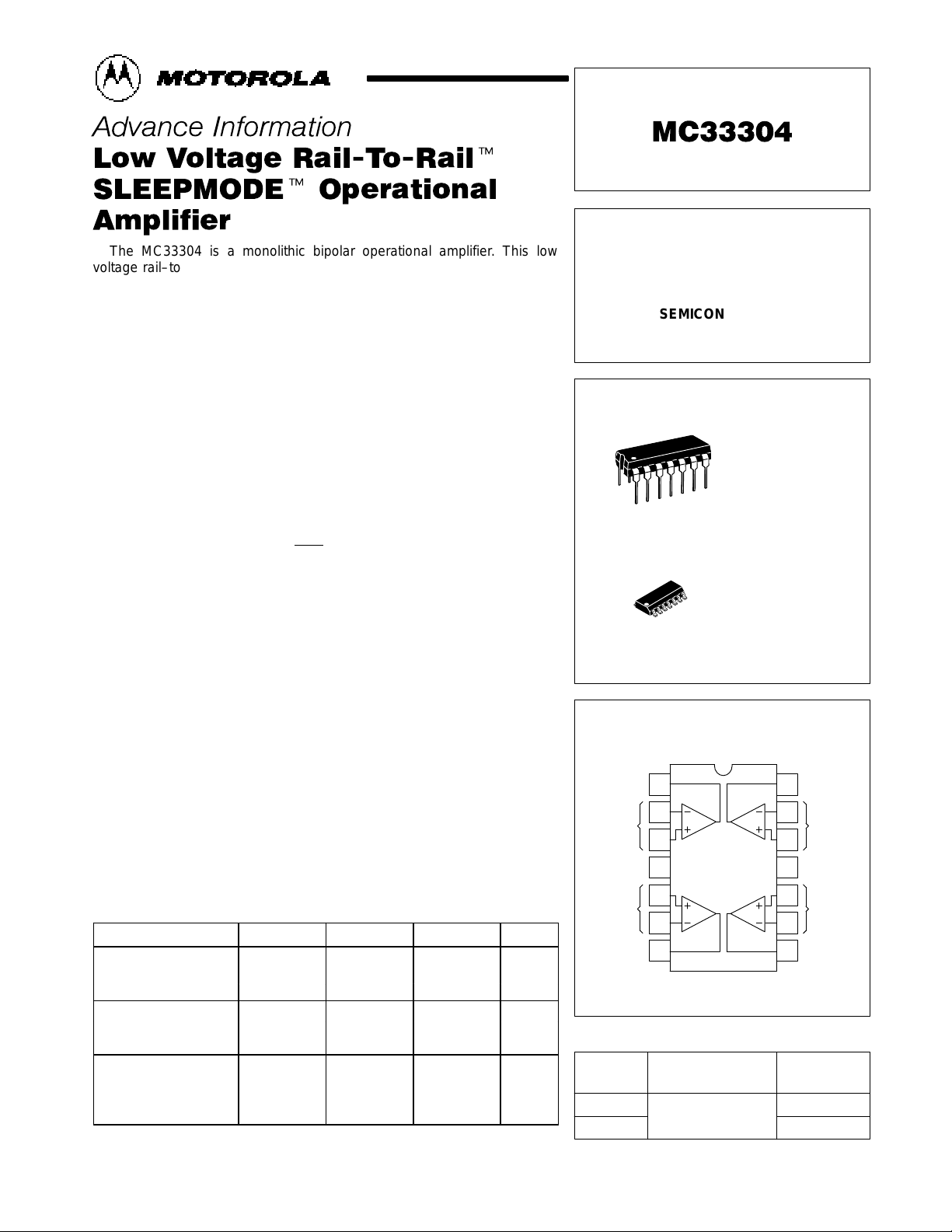
ORDERING INFORMATION
MC33304D
MC33304P
TA = – 40° to +105°C
SO–14
Plastic DIP
P SUFFIX
PLASTIC PACKAGE
CASE 646
14
1
PIN CONNECTIONS
Order this document by MC33304/D
D SUFFIX
PLASTIC PACKAGE
CASE 751A
(SO–14)
14
1
(Quad, Top View)
Output 1
Inputs 1
V
CC
Output 4
Inputs 4
1
12
13
14
11
3
2
1
4
105
96
Output 2
8
7
Inputs 2
2
4
3
V
EE
Inputs 3
Output 3
1
MOTOROLA ANALOG IC DEVICE DATA
t
t
The MC33304 is a monolithic bipolar operational amplifier. This low
voltage rail–to–rail amplifier has both a rail–to–rail input and output stage,
with high output current capability. This amplifier also employs
SLEEPMODE technology. In sleepmode, the micropower amplifier is active
and waiting for an input signal. When a signal is applied, causing the
amplifier to source or sink ≥200 µA (typically) to the load, it will automatically
switch to the awakemode (supplying up to 70 mA to the load). When the
output current drops below 90 µA, the amplifier automatically returns to the
sleepmode.
Excellent performance can be achieved as an audio amplifier. This is due
to the amplifier’s low noise and low distortion. A delay circuit is incorporated
to prevent crossover distortion.
• Ideal for Battery Applications
• Full Output Signal (No Distortion) for Battery Applications Down
to ±0.9 VDC.
• Single Supply Operation (+1.8 to +12 V)
• Rail–To–Rail Performance on Both the Input and Output
• Output Voltages Swings Typically within 100 mV of Both Rails
(RL = 1.0 mΩ)
• Two States: “Sleepmode” (Micropower, I
D
= 110 µA/Amp) and
“Awakemode” (High Performance, ID = 1200 µA/Amp)
• Automatic Return to Sleepmode when Output Current Drops Below
Threshold, Allowing a Fully Functional Micropower Amplifier
• Independent Sleepmode Function for Each Amplifier
• No Phase Reversal on the Output for Overdriven Input Signals
• High Output Current (70 mA typically)
• 600 Ω Drive Capability
• Standard Pinouts; No Additional Pins or Components Required
• Drop–In Replacement for Many Other Quad Operational Amplifiers
• Similar to MC33201, MC33202 and MC33204 Family
• The MC33304 Amplifier is Offered in the Plastic DIP or SOIC Package
(P and D Suffixes)
SLEEPMODE and Rail–To–Rail are trademarks of Motorola, Inc.
TYPICAL DC ELECTRICAL CHARACTERISTICS
(TA = 25°C)
Characteristic
VCC = 2.0 V VCC = 3.3 V VCC = 5.0 V Unit
Input Offset Voltage mV
V
IO(max)
MC33304 ±10 ±10 ±10
Output Voltage Swing
VOH (RL = 600 Ω) 1.85 3.10 4.75 V
min
VOL (RL = 600 Ω) 0.15 0.15 0.15 V
max
Power Supply Current
per Amplifier (ID)
Awakemode 1.625 1.625 1.625 mA
Sleepmode 140 140 140 µA
Specifications are for reference only and not necessarily guaranteed. VEE = Gnd.
Motorola, Inc. 1995
This document contains information on a new product. Specifications and information herein are
subject to change without notice.
Page 2
MC33304
2
MOTOROLA ANALOG IC DEVICE DATA
MAXIMUM RATINGS
Rating Symbol Value Unit
Supply Voltage (VCC to VEE) V
S
+16 V
ESD Protection Voltage at Any Pin
Human Body Model
V
ESD
2000
V
Voltage at Any Device Pin (Note 2) V
DP
VS ± 0.5 V
Input Differential Voltage Range V
IDR
(Notes 1 & 2) V
Output Short Circuit Duration t
s
Indefinite
(Note 3)
sec
Maximum Junction Temperature T
J
+150 °C
Storage Temperature Range T
stg
–65 to +150 °C
Maximum Power Dissipation P
D
(Note 5) mW
RECOMMENDED OPERATING CONDITIONS
Characteristic Symbol Min Typ Max Unit
Supply Voltage V
S
V
Single Supply 1.8 – 12
Split Supplies ±0.9 – ±6.0
Input Voltage Range, Sleepmode and A wakemode V
ICR
V
EE
– V
CC
V
Ambient Operating Temperature Range T
A
–40 – +105 °C
DC ELECTRICAL CHARACTERISTICS (V
CC
= +5.0 V, VEE = Gnd, TA = 25°C, unless otherwise noted.)
Characteristic
Symbol Min Typ Max Unit
Input Offset Voltage (VCM = 0 V, VO = 0 V) (Note 4)
Sleepmode and Awakemode
TA = 25°C
TA = –40° to +105°C
V
IO
–10
–13
0.7
–
+10
+13
mV
Average Temperature Coefficient of Input Offset Voltage
(RS = 50 Ω, VCM = 0 V, VO = 0 V)
TA = –40° to +105°C, Sleepmode and Awakemode
∆VIO/∆T
– 2.0 –
µV/°C
Input Bias Current (VCM = 0 V, VO = 0 V) (Note 4)
Awakemode
TA = 25°C
TA = –40° to +105°C
IIB|
–
–
90
–
+200
+500
nA
Input Offset Current (VCM = 0 V, VO = 0 V) (Note 4)
Awakemode
TA = 25°C
TA = –40° to +105°C
|IIO|
–
–
3.1
–
+50
+100
nA
Large Signal Voltage Gain (VCC = +5.0 V, VEE = –5.0 V)
Awakemode, RL = 600 Ω
TA = 25°C
TA = –40° to +105°C
A
VOL
90
85
116
–
–
–
dB
Power Supply Rejection Ratio, Awakemode PSRR 65 90 – dB
Output Short Circuit Current (Awakemode)
(VID = ±0.2 V)
Source
Sink
I
SC
–200
+50
–89
+89
–50
+200
mA
Output Transition Current, Source/Sink
Sleepmode to Awakemode, VCC = +1.0 V, VEE = –1.0 V
Awakemode to Sleepmode, VCC = +5.0 V, VEE –5.0 V
|I
TH1
|
|I
TH2
|
–
90
–
–
200
–
µA
Page 3
MC33304
3
MOTOROLA ANALOG IC DEVICE DATA
DC ELECTRICAL CHARACTERISTICS (continued) (V
CC
= +5.0 V, VEE = Gnd, TA = 25°C, unless otherwise noted.)
Characteristic UnitMaxTypMinSymbol
Output Voltage Swing (VID = ±0.2 V)
Sleepmode
VCC = +5.0 V, VEE = 0 V, RL = 1.0 MΩ
VCC = 0 V, VEE = –5.0 V, RL = 1.0 MΩ
VCC = +2.0 V, VEE = 0 V, RL = 1.0 MΩ
VCC = 0 V, VEE = –2.0 V, RL = 1.0 MΩ
Awakemode
VCC = +5.0 V, VEE = 0 V, RL = 600 Ω
VCC = 0 V, VEE = –5.0 V, RL = 600 Ω
VCC = +2.0 V, VEE = 0 V, RL = 600 Ω
VCC = 0 V, VEE = –2.0 V, RL = 600 Ω
VCC = +2.5 V, VEE = –2.5 V, RL = 600 Ω
VCC = +2.5 V, VEE = –2.5 V, RL = 600 Ω
V
OH
V
OL
V
OH
V
OL
V
OH
V
OL
V
OH
V
OL
V
OH
V
OL
4.90
–
1.90
–
4.75
–
1.85
–
–
–
4.97
–4.96
1.98
–1.97
4.86
–4.85
1.91
–1.90
2.41
–2.40
–
–4.90
–
–1.90
–
–4.75
–
–1.85
–
–
V
Common Mode Rejection Ratio CMRR 60 90 – dB
Power Supply Current (per Amplifier)
Sleepmode
VCC = +2.0 V, VEE = 0 V TA = +25°C
VCC = +2.5 V, VEE = –2.5 V TA = +25°C
TA = –40° to +105°C
VCC = +12 V, VEE = 0 V TA = +25°C
Awakemode
VCC = +2.5 V, VEE = –2.5 V TA = +25°C
TA = –40° to +105°C
I
D
–
–
–
–
–
–
85
110
–
125
1200
–
–
140
150
–
1625
1750
µA
Thermal Resistance
SOIC
Plastic DIP
θ
JA
–
–
145
75
–
–
°C/W
AC ELECTRICAL CHARACTERISTICS (V
CC
= +6.0 V, VEE = –6.0 V, RL = 600 Ω, TA = 25°C, unless otherwise noted.)
Characteristic
Symbol Min Typ Max Unit
Slew Rate (VCC = +2.5 V, VEE = –2.5 V, AV = +1.0) (Note 6)
Awakemode
SR
0.5 0.89 –
V/µs
Gain Bandwidth Product (f = 100 kHz)
Awakemode
GBW
– 2.2 –
MHz
Gain Margin (CL = 0 pF)
Awakemode
Sleepmode (RL = 1.0 kΩ)
A
m
–
–
6.0
9.0
–
–
dB
Phase Margin (RL = 1.0 kΩ, VO = 0 V, CL = 0 pF)
Awakemode
Sleepmode
φ
m
–
–
40
60
–
–
Deg
Sleepmode to Awakemode Transition Time
RL = 600 Ω
RL = 10 k
t
tr1
–
–
4.0
12
–
–
µsec
Awakemode to Sleepmode Transition Time t
tr2
– 1.5 – sec
Channel Separation (f = 1.0 kHz)
Awakemode
CS
– 100 –
dB
NOTES: 1. The differential input voltage of each amplifier is limited by two internal diodes. The diodes are connected across the inputs in parallel and opposite to
each other. For more differential input voltage range, use current limiting resistors in series with the input pins.
2.The common–mode input voltage range of each amplifier is limited by diodes connected from the inputs to both power supply rails. Therefore, the
voltage on either input must not exceed supply rail by more than ±500 mV.
3.Simultaneous short circuits of two or more amplifiers to the positive or negative rail can exceed the power dissipation ratings and cause eventual
failure of the device.
4.Rail–to–rail performance is achieved at the input of the amplifier by using parallel NPN–PNP differential stages. When the inputs are near the
negative rail (VEE < VCM < 800 mV), the PNP stage is on. When the inputs are above 800 mV (i.e. 800 mV < VCM < VCC), the NPN stage is on.
This switching of the input pairs will cause a reversal of input bias current. Slight changes in the input offset voltage will be noted between the NPN
and PNP pairs. Cross–coupling techniques have been used to keep this change to a minimum.
5.Power dissipation must be considered to ensure maximum junction (TJ) is not exceeded. (See Figure 2)
6.When connected as a voltage follower and used in transient conditions, a current limiting resistor may be needed between the output and the
inverting input. This is because of the back to back diodes clamped across the inputs. The value of this resistor should be between 1.0 kΩ and
10 kΩ. If the amplifier does not become slew rate limited and is processing low frequency waveforms, then no resistor would be necessary.
(The output could be tied directly to the negative input.)
Page 4
MC33304
4
MOTOROLA ANALOG IC DEVICE DATA
AC ELECTRICAL CHARACTERISTICS
(continued) (VCC = +6.0 V, VEE = –6.0 V, RL = 600 Ω, TA = 25°C, unless otherwise noted.)
Characteristic UnitMaxTypMinSymbol
Power Bandwidth (VO = 4.0 V
pp, RL
= 2.0 kΩ, THD ≤ 1.0%)
Awakemode
BW
p
– 28 –
kHz
Distortion (VO = 2.0 Vpp, AV = +1.0)
Awakemode (f = 10 kHz)
Sleepmode (f = 1.0 kHz, RL = Infinite)
THD
–
–
0.009
0.007
–
–
%
Open Loop Output Impedance
(VO = 0 V, f = 2.0 MHz, AV = +10, IQ = 10 µA)
Awakemode
Sleepmode
|ZO|
–
–
100
1000
–
–
Ω
Differential Input Impedance (VCM = 0 V)
Awakemode
Sleepmode
R
IN
–
–
200
1300
–
–
kΩ
Differential Input Capacitance (VCM = 0 V)
Awakemode
Sleepmode
C
IN
–
–
8.0
0.4
–
–
pF
Equivalent Input Noise Voltage (RS = 100 Ω, f = 1.0 kHz)
Awakemode
Sleepmode
e
n
–
–
15
60
–
–
nVńHz
Ǹ
Equivalent Input Noise Current (f = 1.0 kHz)
Awakemode
Sleepmode
i
n
–
–
0.22
0.20
–
–
pAńHz
Ǹ
NOTES: 1. The differential input voltage of each amplifier is limited by two internal diodes. The diodes are connected across the inputs in parallel and opposite to
each other. For more differential input voltage range, use current limiting resistors in series with the input pins.
2.The common–mode input voltage range of each amplifier is limited by diodes connected from the inputs to both power supply rails. Therefore, the
voltage on either input must not exceed supply rail by more than ±500 mV.
3.Simultaneous short circuits of two or more amplifiers to the positive or negative rail can exceed the power dissipation ratings and cause eventual
failure of the device.
4.Rail–to–rail performance is achieved at the input of the amplifier by using parallel NPN–PNP differential stages. When the inputs are near the
negative rail (VEE < VCM < 800 mV), the PNP stage is on. When the inputs are above 800 mV (i.e. 800 mV < VCM < VCC), the NPN stage is on.
This switching of the input pairs will cause a reversal of input bias current. Slight changes in the input offset voltage will be noted between the NPN
and PNP pairs. Cross–coupling techniques have been used to keep this change to a minimum.
5.Power dissipation must be considered to ensure maximum junction (TJ) is not exceeded. (See Figure 2)
6.When connected as a voltage follower and used in transient conditions, a current limiting resistor may be needed between the output and the
inverting input. This is because of the back to back diodes clamped across the inputs. The value of this resistor should be between 1.0 kΩ and
10 kΩ. If the amplifier does not become slew rate limited and is processing low frequency waveforms, then no resistor would be necessary.
(The output could be tied directly to the negative input.)
Page 5

MC33304
5
MOTOROLA ANALOG IC DEVICE DATA
Figure 1. Equivalent Circuit Block Diagram (Each Amplifier)
Current
Threshold
Detector
Awake to
Sleepmode
Delay Circuit
Awakemode
Current
Regulator
Sleepmode
Current
Regulator
Fractional
Load Current
Detector
I
Hysteresis
I
Enable
Enable
Bias
Bias
Boost
Interface
Stage
Output
Stage
Input
Stage
Buffer
C
Storage
Buffer
Overdrive
Correction
V
in
% of I
L
I
Awake
I
Sleep
I
Bias
I
ref
I
L
V
out
R
L
There are 515 active components for the entire quad device.
Page 6

MC33304
6
MOTOROLA ANALOG IC DEVICE DATA
DEVICE DESCRIPTION
The MC33304 will begin to function at power supply
voltages as low as VS = ±0.8 V. The device has the ability to
swing rail–to–rail on both the input and the output. Since the
common mode input voltage range extends from VCC to VEE,
it can be operated with either single or split voltage supplies.
The MC33304 is guaranteed not to latch up or phase reverse
over the entire common mode range. However, the output
could go into phase reversal state if input voltage is set higher
than +VCC or –VEE.
When power is initially applied, the part may start to
operate in the awakemode. This occurs because of bias
currents being generated from the charging of the internal
capacitors. When this occurs, the user will have to wait
approximately 1.5 seconds before the device will switch back
to the sleepmode.
The amplifier is designed to switch from sleepmode to
awakemode whenever the output current exceeds a preset
current threshold (ITH) of approximately 200 µA. As a result,
the output switching threshold voltage (VST) is controlled by
the output loading resistance (RL). Large valued load
resistors require a large output voltage to switch, but reduce
unwanted transitions to the awakemode.
Most of the transition time is consumed slewing in the
sleepmode until VST is reached, therefore, small values of R
L
allow rapid transition to the awakemode. The output
switching threshold voltage (VST) is higher for the larger
values of RL, requiring the amplifier to slew longer in the
slower sleepmode state before switching to the awakemode.
Although typically 200 µA, ITH varies with supply voltage,
temperature and the load resistance. Generally, any current
loading on the ouput which causes a current greater than I
TH
to flow will switch the amplifier into the awakemode. This
includes transition currents like those generated by charging
load capacitances. In fact, the maximum capacitance that
can be driven while attempting to remain in the sleepmode is
approximately 300 pF.
The awakemode to sleepmode transition time is controlled
by an internal delay circuit, which is necessary to prevent the
amplifier from going to sleep during every zero crossing of
the output waveform. This delay circuit also eliminates the
crossover distortion commonly found in micropower
amplifiers.
The MC33304 rail–to–rail sleepmode operational amplifier
is unique in its ability to swing rail–to–rail on both the input
and output using a bipolar design. This offers a low noise and
wide common mode input voltage range. Since the common
mode input voltage range extends from VCC to VEE, it can be
operated with either single or split voltage supplies.
Rail–to–rail performance is achieved at the input of the
amplifiers by using parallel NPN–PNP differential input
stages. When the inputs are within 800 mV of the negative
rail, the PNP stage is on. When the inputs are more than
800 mV above VEE, the NPN stage is on. This switching of
input pairs will cause a reversal of input bias currents. Also,
slight differences in offset voltage may be noted between the
NPN and PNP pairs. Cross–coupling techniques have been
used to keep this change to a minimum.
In addition to the rail–to–rail performance, the output stage
is current boosted to provide enough output current to drive
600 Ω loads. Because of this high current capability, care
should be taken not to exceed the 150°C maximum junction
temperature specification.
Page 7

MC33304
7
MOTOROLA ANALOG IC DEVICE DATA
MC33304P
MC33304P
, MAXIMUM POWER DISSIPATION (mW)
D(max)
P
–55
2.5 k
TA, AMBIENT TEMPERATURE (
°
C)
–40 –25 0 25 50 85 125
2.0 k
1.5 k
1.0 k
0.5 k
0
–55
150
I
IB
, INPUT BIAS CURRENT (nA)
TA, AMBIENT TEMPERATURE (°C)
VCC = +5.0 V
VEE = Gnd
VCM = 0 V
Awakemode
–40 –25 0 25 50 85 125
135
120
105
90
75
VCC = +5.0 V
VEE = Gnd
RL = 600
Ω
∆
VO = 0.5 to 4.5 V
Awakemode
–55
130
A
VOL
, OPEN LOOP VOLTAGE GAIN (dB)
TA, AMBIENT TEMPERATURE (°C)
1258550250–25–40
120
110
100
90
80
12
10
6.0
2.0
0
VCC,VEE
SUPPLY VOLTAGE (V)
8.0
V
O
, OUTPUT VOLTAGE (V )
pp
4.0
±
1.0
±
2.0
±
3.0
±
4.0
±
5.0
±
6.0
RL = 600 Ω – 1.0 M
Ω
TA = 25°C
Awakemode/
Sleepmode
0.1
12
f, FREQUENCY (kHz)
V
O
, OUTPUT VOLTAGE SWING (V )
pp
Sleepmode
(RL = 1.0 M
Ω
)
Awakemode
(RL = 600
Ω
)
VCC = +6.0 V
VEE = –6.0 V
AV = +1.0
TA = 25
°
C
1.0 k100101.0
10
8.0
6.0
4.0
2.0
0
–6.0
100
I
IB
, INPUT BIAS CURRENT (nA)
VCM, COMMON MODE INPUT VOLTAGE (V)
TA = 25°C
VCC = +5.0 V
VEE = Gnd
Sleepmode
Awakemode
–4.0 –2.0 0 2.0 4.0 6.0
50
0
–50
–100
–150
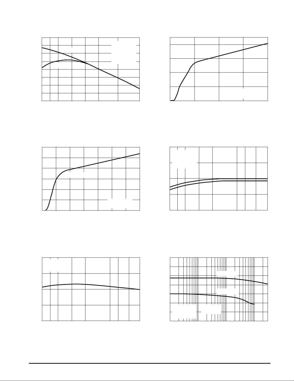
Figure 2. Maximum Power Dissipation
versus Temperature
Figure 3. Input Bias Current versus Temperature
Figure 4. Input Bias Current versus
Common Mode Input Voltage
Figure 5. Open Loop Voltage Gain
versus Temperature
Figure 6. Output Voltage Swing
versus Supply Voltage
Figure 7. Output Voltage versus Frequency
Page 8

MC33304
8
MOTOROLA ANALOG IC DEVICE DATA
10
100
V
O
, OUTPUT VOLTAGE SWING (V )
RL, LOAD RESISTANCE TO GROUND (Ω)
Figure 8. Maximum Peak–to–Peak Output
Voltage Swing versus Load Resistance
VCC = +6.0 V
VEE = –6.0 V
f = 1.0 kHz
TA = 25
°
C
pp
100 1.0 k 10 k 100 k
10
1.0
0.1
10
100
CMR, COMMOM MODE REJECTION (dB)
f, FREQUENCY (Hz)
Figure 9. Common Mode Rejection
versus Frequency
VCC = +6.0 V
VEE = –6.0 V
TA = 25
°
C
Sleepmode
Awakemode
100 1.0 k 10 k 100 k 1.0 m 10 m
80
60
40
20
0
10
80
PSR, POWER SUPPLY REJECTION (dB)
f, FREQUENCY (Hz)
Figure 10. Power Supply Rejection
versus Frequency
VCC = +6.0 V
VEE = –6.0 V
TA = 25
°
C
±
PSR
Awakemode
±
PSR
Sleepmode
60
40
20
0
100 1.0 k 10 k 100 k 1.0 M 10 M
0
240
I
TH2
, CURRENT THRESHOLD ( A)
µ
VCC, VEE
, SUPPLY VOLTAGE (V)
Figure 11. Awakemode to Sleepmode
Current Threshold versus Supply Voltage
TA = 125°C
TA = 25°C
TA = –55°C
Source Current
1.0 2.0 3.0 4.0 5.0 6.0
200
160
120
80
TH1
, CURRENT THRESHOLD ( A)
µ
0
260
Figure 12. Sleepmode to Awakemode
Current Threshold versus Supply Voltage
TA = 25°C
TA = –55°C
TA = 125°C
Source Current
VCC,
VEE
, SUPPLY VOLTAGE (V)
1.0 2.0 4.0 5.03.0 6.0 7.0
240
220
200
180
160
0
80
SC
IVOI, OUTPUT VOLTAGE (V)
Figure 13. Output Short Circuit Current
versus Output Voltage
VCC = +6.0 V
VEE = –6.0 V
VID =
±
1.0 V
Awakemode
Source
Sink
2.0 4.0 6.0
70
60
50
40
, OUTPUT SHORT CIRCUIT CURRENT (mA)
I
I
Page 9
MC33304
9
MOTOROLA ANALOG IC DEVICE DATA
VCC = + 2.5 V
VEE = – 2.5 V
f = 100 kHz
GBW, GAIN BANDWIDTH PRODUCT (MHz)
TA, AMBIENT TEMPERATURE (°C)
4.0
3.0
2.0
0
1.0
–55 –40 –25 25 70 1250 85 105
Source
Sink
–55
120
TA, AMBIENT TEMPERATURE (
°
C)
VCC = +5.0 V
VEE = Gnd
VID =
±
0.2 V
RL = 1.0 M
Ω
Awakemode
–40 –25 0 25 50 85 125
100
80
60
40
0
VCC, SUPPLY VOLTAGE (V)
Single Supply
RL = 600
Ω
3.5 7.0 10.5 14
3.0 k
2.0 k
1.0 k
0
4.0 k
0
600
Single Supply
No Load
Sleepmode (µA)
SUPPLY CURRENT ( A)
µ
2.0 4.0 6.0 8.0 10 12 14
500
400
300
200
100
0
–55
2.0
SR, SLEW RATE (V/ s)
µ
TA, AMBIENT TEMPERATURE (°C)
VCC = +2.5 V
VEE = –2.5 V
VO =
±
2.0 V
RL= 600
Ω
+ Slew Rate
– Slew Rate
–25 25 70 1250 85 105–40
1.5
1.0
0.5
0
10
14
A
m
, GAIN MARGIN (dB)
RT, DIFFERENTIAL SOURCE RESISTANCE (Ω)
VCC = +6.0 V
VEE = –6.0 V
RT = R1 + R2
VO = 0 V
TA = 25
°
C
Sleepmode
Awakemode
100 1.0 k 10 k
12
10
8.0
6.0
4.0
2.0
0
Figure 14. Output Short Circuit Current
versus Temperature
Figure 15. Supply Current versus
Supply Voltage with Load
Figure 16. Supply Current versus Supply Voltage
Figure 17. Slew Rate versus Temperature
Figure 18. Gain Bandwidth Product
versus Temperature
Figure 19. Gain Margin versus
Differential Source Resistance
V , SUPPLY VOLTAGE (V)
CC
I ,
D
SC
, OUTPUT SHORT CIRCUIT CURRENT (mA)
I
µ
SUPPLY CURRENT ( A)
D
I ,
Page 10

MC33304
10
MOTOROLA ANALOG IC DEVICE DATA
10
80
φ
m
, PHASE MARGIN ( )
°
RT, DIFFERENTIAL SOURCE RESISTANCE (Ω)
Sleepmode
Awakemode
VCC = +6.0 V
VEE = –6.0 V
RT = R1 + R2
VO = 0 V
TA = 25
°
C
10 k1.0 k100
70
60
50
40
30
20
10
10
70
PHASE MARGIN ( )
CL, OUTPUT LOAD CAPACITANCE (pF)
°
Sleepmode
Awakemode
1.0 k100
60
50
40
30
20
10
0
10
9.0
A
CL, OUTPUT LOAD CAPACITANCE (pF)
Sleepmode
Awakemode
VCC = +6.0 V
VEE = –6.0 V
100 1.0 k
7.0
5.0
3.0
1.0
m
, GAIN MARGIN (dB)
100
140
CS, CHANNEL SEPARATION (dB)
f, FREQUENCY (Hz)
VCC = +6.0 V
VEE = –6.0 V
RL = 600
Ω
Awakemode
1.0 k 10 k 100 k
120
100
80
60
40
20
0
100
100
THD, TOTAL HARMONIC DISTORTION (%)
f, FREQUENCY (Hz)
VCC = +6.0 V
VEE = –6.0 V
RL = 600
Ω
VO = 2.0 V
pp
TA = 25
°
C
Awakemode
AV = 1000
AV = 100
AV = 10
AV = 1.0
1.0 k 10 k 100 k
10
1.0
0.1
0.01
0.001
10
100
e
n
, INPUT REFERRED NOISE VOLTAGE (nV/ Hz)
√
f, FREQUENCY (Hz)
Sleepmode
Awakemode
VCC = +6.0 V
VEE = –6.0 V
TA = 25
°
C
100 k10 k1.0 k100
80
60
40
20
10
Figure 20. Phase Margin versus
Differential Source Resistance
Figure 21. Gain Margin versus
Output Load Capacitance
Figure 22. Phase Margin versus
Output Load Capacitance
Figure 23. Channel Separation
versus Frequency
Figure 24. Total Harmonic Distortion
versus Frequency
Figure 25. Input Referred Noise Voltage
versus Frequency
Page 11

MC33304
11
MOTOROLA ANALOG IC DEVICE DATA
10
1.4
i
n
, INPUT NOISE CURRENT (pA/ Hz)
f, FREQUENCY (Hz)
Figure 26. Current Noise versus Frequency
√
Sleepmode
Awakemode
VCC = +6.0 V
VEE = –6.0 V
TA = 25
°
C
(RS = 100 k)
100 1.0 k 10 k 100 k
1.2
1.0
0.8
0.6
0.4
0.2
0
10
100
OS, PERCENT OVERSHOOT (%)
CL, LOAD CAPACITANCE (pF)
Figure 27. Percent Overshoot
versus Load Capacitance
VCC = +6.0 V
VEE = –6.0 V
TA = 25
°
C
Sleepmode
(RL =
∞
)
Awakemode
(RL = 600
Ω
)
80
60
40
20
0
100 1.0 k
Page 12

MC33304
12
MOTOROLA ANALOG IC DEVICE DATA
OUTLINE DIMENSIONS
P SUFFIX
PLASTIC PACKAGE
CASE 646–06
ISSUE L
D SUFFIX
PLASTIC PACKAGE
CASE 751A–03
(SO–14)
ISSUE F
NOTES:
1. LEADS WITHIN 0.13 (0.005) RADIUS OF TRUE
POSITION AT SEATING PLANE AT MAXIMUM
MATERIAL CONDITION.
2. DIMENSION L TO CENTER OF LEADS WHEN
FORMED PARALLEL.
3. DIMENSION B DOES NOT INCLUDE MOLD
FLASH.
4. ROUNDED CORNERS OPTIONAL.
1 7
14 8
B
A
F
H G D
K
C
N
L
J
M
SEATING
PLANE
DIM MIN MAX MIN MAX
MILLIMETERSINCHES
A 0.715 0.770 18.16 19.56
B 0.240 0.260 6.10 6.60
C 0.145 0.185 3.69 4.69
D 0.015 0.021 0.38 0.53
F 0.040 0.070 1.02 1.78
G 0.100 BSC 2.54 BSC
H 0.052 0.095 1.32 2.41
J 0.008 0.015 0.20 0.38
K 0.115 0.135 2.92 3.43
L 0.300 BSC 7.62 BSC
M 0 10 0 10
N 0.015 0.039 0.39 1.01
_ _ _ _
NOTES:
1. DIMENSIONING AND TOLERANCING PER ANSI
Y14.5M, 1982.
2. CONTROLLING DIMENSION: MILLIMETER.
3. DIMENSIONS A AND B DO NOT INCLUDE
MOLD PROTRUSION.
4. MAXIMUM MOLD PROTRUSION 0.15 (0.006)
PER SIDE.
5. DIMENSION D DOES NOT INCLUDE DAMBAR
PROTRUSION. ALLOWABLE DAMBAR
PROTRUSION SHALL BE 0.127 (0.005) TOTAL
IN EXCESS OF THE D DIMENSION AT
MAXIMUM MATERIAL CONDITION.
–A–
–B–
G
P
7 PL
14 8
71
M
0.25 (0.010) B
M
S
B
M
0.25 (0.010) A
S
T
–T–
F
R
X 45
SEATING
PLANE
D 14 PL
K
C
J
M
_
DIM MIN MAX MIN MAX
INCHESMILLIMETERS
A 8.55 8.75 0.337 0.344
B 3.80 4.00 0.150 0.157
C 1.35 1.75 0.054 0.068
D 0.35 0.49 0.014 0.019
F 0.40 1.25 0.016 0.049
G 1.27 BSC 0.050 BSC
J 0.19 0.25 0.008 0.009
K 0.10 0.25 0.004 0.009
M 0 7 0 7
P 5.80 6.20 0.228 0.244
R 0.25 0.50 0.010 0.019
_ _ _ _
Motorola reserves the right to make changes without further notice to any products herein. Motorola makes no warranty, representation or guarantee regarding
the suitability of its products for any particular purpose, nor does Motorola assume any liability arising out of the application or use of any product or circuit,
and specifically disclaims any and all liability, including without limitation consequential or incidental damages. “T ypical” parameters can and do vary in different
applications. All operating parameters, including “T ypicals” must be validated for each customer application by customer’s technical experts. Motorola does
not convey any license under its patent rights nor the rights of others. Motorola products are not designed, intended, or authorized for use as components in
systems intended for surgical implant into the body, or other applications intended to support or sustain life, or for any other application in which the failure of
the Motorola product could create a situation where personal injury or death may occur. Should Buyer purchase or use Motorola products for any such
unintended or unauthorized application, Buyer shall indemnify and hold Motorola and its officers, employees, subsidiaries, affiliates, and distributors harmless
against all claims, costs, damages, and expenses, and reasonable attorney fees arising out of, directly or indirectly, any claim of personal injury or death
associated with such unintended or unauthorized use, even if such claim alleges that Motorola was negligent regarding the design or manufacture of the part.
Motorola and are registered trademarks of Motorola, Inc. Motorola, Inc. is an Equal Opportunity/Affirmative Action Employer.
How to reach us:
USA /EUROPE: Motorola Literature Distribution; JAPAN: Nippon Motorola Ltd.; Tatsumi–SPD–JLDC, Toshikatsu Otsuki,
P.O. Box 20912; Phoenix, Arizona 85036. 1–800–441–2447 6F Seibu–Butsuryu–Center, 3–14–2 Tatsumi Koto–Ku, Tokyo 135, Japan. 03–3521–8315
MFAX: RMFAX0@email.sps.mot.com – TOUCHTONE (602) 244–6609 HONG KONG: Motorola Semiconductors H.K. Ltd.; 8B Tai Ping Industrial Park,
INTERNET: http://Design–NET.com 51 Ting Kok Road, Tai Po, N.T., Hong Kong. 852–26629298
MC33304/D
*MC33304/D*
◊
 Loading...