

Page 1
Device
Tested Operating
Temperature Range
Package
SEMICONDUCTOR
TECHNICAL DATA
OCTAL SERIAL SWITCH
(SPI Input/Output)
ORDERING INFORMATION
MC33298P
MC33298DW
TC = – 40° to +125°C
DIP
SOP–24L
Order this document by MC33298/D
P SUFFIX
PLASTIC PACKAGE
CASE 738
DIP (16+2+2)
PIN CONNECTIONS
20
1
DW SUFFIX
PLASTIC PACKAGE
CASE 751E
SOP (16+4+4)L
24
1
DIP Function SOP–24L
1
2
3
4
5
6
–
–
7
8
9
10
11
12
13
14
15
16
–
–
17
18
19
20
Output 7
Output 6
SCLK
SI
Ground
Ground
Ground
Ground
SO
CSB
Output 5
Output 4
Output 3
Output 2
SFPD
V
DD
Ground
Ground
Ground
Ground
V
PWR
Reset
Output 1
Output 0
1
2
3
4
5
6
7
8
9
10
11
12
13
14
15
16
17
18
19
20
21
22
23
24
1
MOTOROLA ANALOG IC DEVICE DATA
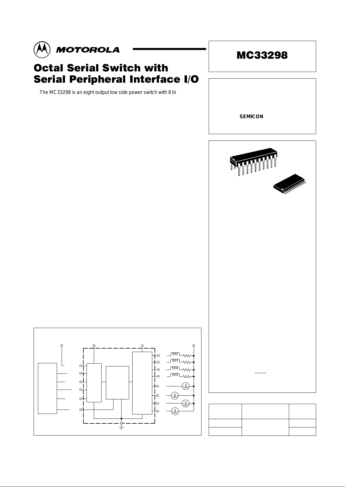
The MC33298 is an eight output low side power switch with 8 bit serial input
control. The MC33298 is a versatile circuit designed for automotive
applications, but is well suited for other environments. The MC33298
incorporates SMARTMOS technology, with CMOS logic, bipolar/MOS
analog circuitry, and DMOS power MOSFETs. The MC33298 interfaces
directly with a microcontroller to control various inductive or incandescent
loads. The circuit’s innovative monitoring and protection features are: very low
standby current, cascadable fault reporting, internal 65 V clamp on each
output, output specific diagnostics, and independent shutdown of outputs. The
MC33298 is parametrically specified over a temperature range of – 40°C ≤ T
A
≤ +125°C ambient temperature and 9.0 V ≤ V
PWR
≤ 16 V supply. The
economical 20 pin DIP and SO–24 wide body surface mount plastic packages
make the MC33298 very cost effective.
• Designed to Operate Over Wide Supply Voltages of 5.5 V to 26.5 V
• Interfaces Directly to Microprocessor Using SPI Protocol
• SPI Communication for Control and Fault Reporting
• 8–Bit Serial I/O is CMOS Compatible
• 3.0 A Peak Current Outputs with Maximum R
DS(on)
of 0.45 Ω at 25°C
• Outputs are Current Limited to 3.0 A to 6.0 A for Driving Incandescent
Lamp Loads
• Output Voltages Clamped to 65 V During Inductive Switching
• Maximum Sleep Current (I
PWR
) of 50 µA with VDD ≤ 2.0 V
• Maximum of 4.0 mA I
DD
During Operation
• Maximum of 2.0 mA I
PWR
During Operation with All Outputs “On”
• Open Load Detection (Outputs “Off”)
• Overvoltage Detection and Shutdown
• Each Output has Independent Over Temperature Detection and Shutdown
• Output Mode Programmable for Sustained Current Limit or Shutdown
• Short Circuit Detect and Shutdown with Automatic Retry for Every
Write Cycle
• Serial Operation Guaranteed to 2.0 MHz
Micro–
controller
with Bus
+V
bat
SCLK
CSB
SFPD
SO
V
PWR
V
DD
CMOS
Serial Shift
Registers
and
Latches
CMOS
Input
Logic
Updrain
DMOS
Output
Switches
and
Sense
Circuits
SI
Reset
SFPD
Y
0
Y
1
Y
2
Y
3
Y
4
Y
5
Y
6
Y
7
Gnd
This device contains 1,200 active transistors.
Simplified Application
Motorola, Inc. 1996 Rev 2
Page 2
MC33298
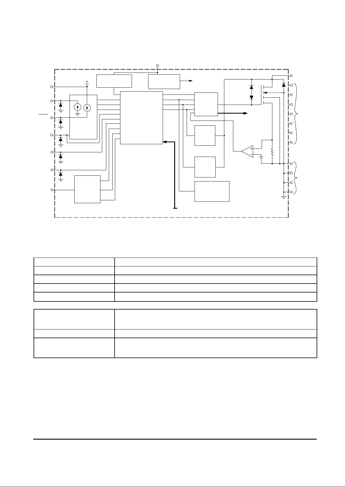
2
MOTOROLA ANALOG IC DEVICE DATA
I
Limit
Output 0
R
S
Open
Load
Detect
Short
Circuit
Detect
Over
Temperature
Detect
SO
SI
SCLK
CSB
Reset
SFPD
V
DD
Gate
Control
65 V
Outputs
1–7
Grounds
Figure 1. Simplified Block Diagram
Overvoltage
Detect
Voltage
Regulator
Fault
Timers
OVD
RB
SFPDB
SFL
CSB
SCLK
SI
SO
CSI
CSBI
To Gates
1–7
From Detectors 1 to 7
V
PWR
Serial D/O
Line Driver
SPI
Interface
Logic
GE
OT
SF
OF
20
µ
A
20
µ
A
Bias
FAULT OPERATION
SERIAL OUTPUT (SO) PIN REPORTS
Overvoltage
Overvoltage condition reported.
Over Temperature Fault reported by Serial Output (SO) pin.
Over Current SO pin reports short to battery/supply or over current condition.
Output “On,” Open Load Fault Not reported.
Output “Off,” Open Load Fault SO pin reports output “off” open load condition.
DEVICE SHUTDOWNS
Overvoltage Total device shutdown at V
PWR
= 28–36 V. Re–operates when overvoltage is removed with
all outputs assuming an off state upon recovery from overvoltage. All device registers are
automatically reset (cleared) during shutdown.
Over Temperature Only the output experiencing an over temperature shuts down.
Over Current Only the output experiencing an over current condition shuts down at 3.0 A to 6.0 A after a
25 µs to 100 µs delay, with SFPD pin grounded. All outputs will continue to operate in a current
limit mode, with no shutdown, if the SPFD pin is at 5.0 V.
Page 3
MC33298
3
MOTOROLA ANALOG IC DEVICE DATA
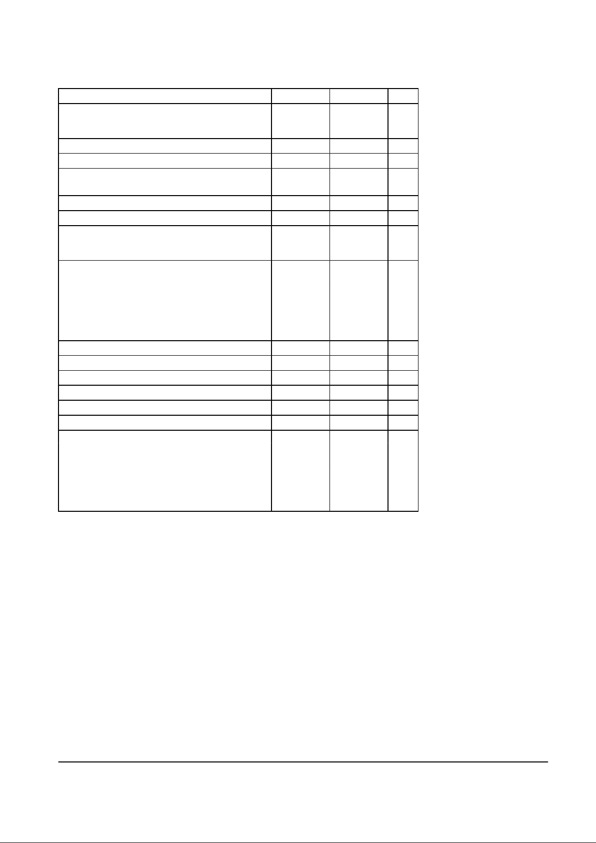
MAXIMUM RATINGS (All voltages are with respect to ground, unless otherwise noted.)
Rating Symbol Value Unit
Power Supply Voltage
Steady–State V
PWR(sus)
–1.5 to 26.5 V
Transient Conditions (Note1) V
PWR(pk)
–13 to 60 V
Logic Supply Voltage (Note 2) V
DD
– 0.3 to 7.0 V
Input Pin Voltage (Note 3) V
IN
– 0.3 to 7.0 V
Output Clamp Voltage (Note 4) V
OUT(off)
V
(2.0 mA ≤ I
out
≤ 0.5 A) 50 to 75
Output Self–Limit Current I
OUT(lim)
3.0 to 6.0 A
Continuous Per Output Current (Note 5) I
OUT(cont)
1.0 A
ESD Voltage
Human Body Model (Note 6) V
ESD1
2000 V
Machine Model (Note 7) V
ESD2
200 V
Output Clamp Energy (Note 8) E
clamp
Repetitive:
TJ =25°C 100 mJ
TJ = 125°C 30 mJ
Non–Repetitive:
TJ =25°C 2.0 J
TJ = 125°C 0.5 J
Recommended Frequency of SPI Operation (Note 9) f
SPI
2.0 MHz
Storage Temperature T
stg
– 55 to +150 °C
Operating Case Temperature T
C
– 40 to +125 °C
Operating Junction Temperature T
J
– 40 to +150 °C
Power Dissipation (TA =25°C) (Note 10) P
D
3.0 W
Soldering Temperature (for 10 seconds) T
solder
260 °C
Thermal Resistance, Junction–to–Ambient (Note 11) R
θJA
°C/W
Plastic Package, Case 738:
All Outputs “On” (Note 12) 31
Single Output “On” (Note 13) 37
SOP–24 Package, Case 751E:
All Outputs “On” (Note 12) 34
Single Output (Note 13) 40
NOTES: 1. Transient capability with external 100 Ω resistor connected in series with V
PWR
pin and supply.
2. Exceeding these limits may cause a malfunction or permanent damage to the device.
3. Exceeding voltage limits on SCLK, SI, CSB, SFPD, or Reset pins may cause permanent damage to
the device.
4. With output “off.”
5. Continuous output rating so long as maximum junction temperature is not exceeded. (See Figure 21 and
22 for more details).
6. ESD1 testing is performed in accordance with the Human Body Model (C
Zap
= 100 pF, R
Zap
= 1500 Ω).
7. ESD2 testing is performed in accordance with the Machine Model (C
Zap
= 100 pF, R
Zap
= 0 Ω).
8. Maximum output clamp energy capability at indicated Junction Temperature using single pulse method.
See Figure 19 for more details.
9. Guaranteed and production tested for 2.0 MHz SPI operation but has been demonstrated to operate to
8.5 MHz @ 25°C.
10. Maximum power dissipation at indicated junction temperature with no heat sink used. See Figures 20,
21, and 22 for more details.
11. See Figure 20 for Thermal Model.
12. Thermal resistance from Junction–to–Ambient with all outputs “on” and dissipating equal power.
13. Thermal resistance from Junction–to–Ambient with a single output “on.”
Page 4
MC33298
4
MOTOROLA ANALOG IC DEVICE DATA
STATIC ELECTRICAL CHARACTERISTICS
(Characteristics noted under conditions of 4.5 V ≤ VDD ≤ 5.5 V, 9.0 V ≤V
PWR
≤ 16 V,
–40°C ≤ TC ≤ 125°C, unless otherwise noted.)
Characteristic
Symbol Min Typ Max Unit
POWER INPUT
Supply Voltage Range V
Quasi–Functional (Note 1) V
PWR(qf)
5.5 – 9.0
Full Operational V
PWR(fo)
9.0 – 26.5
Supply Current (all Outputs “On,” I
out
= 0.5 A) (Note 2) I
PWR(on)
– 1.0 2.0 mA
Sleep State Supply Current (VDD
=0.5 V)
I
PWR(ss)
– 1.0 50 µA
Sleep State Output Leakage Current (per Output, VDD = 0.5 V) I
OUT(ss)
– – 50 µA
Overvoltage Shutdown V
OV
28 – 36 V
Overvoltage Shutdown Hysteresis V
OV(hys)
0.2 – 1.5 V
Logic Supply Voltage V
DD
4.5 – 5.5 V
Logic Supply Current (with any combination of Outputs “On”) I
DD
– – 4.0 mA
Logic Supply Undervoltage Lockout Threshold (Note 3) V
DD(uvlo)
2.0 – 4.5 V
POWER OUTPUT
Drain–to–Source “On” Resistance (I
out
= 0.5 A, TJ =25°C) R
DS(on)
Ω
V
PWR
= 5.5 V – – 1.0
V
PWR
= 9.0 V – 0.4 0.5
V
PWR
= 13 V – 0.35 0.45
Drain–to–Source “On” Resistance (I
out
= 0.5 A, TJ = 150°C) R
DS(on)
Ω
V
PWR
= 5.5 V – – 1.8
V
PWR
= 9.0 V – 0.75 0.9
V
PWR
= 13 V – 0.65 0.8
Output Self–Limiting Current I
OUT(lim)
A
Outputs Programmed “On”, V
out
= 0.6 V
DD
3.0 4.0 6.0
Output Fault Detect Threshold (Note 4) V
OUTth(F)
V
DD
Output Programmed “Off” 0.6 0.7 0.8
Output “Off” Open Load Detect Current (Note 5) I
OCO
µA
Output Programmed “Off,” V
out
= 0.6 V
DD
30 50 100
Output Clamp Voltage V
OK
V
2.0 mA ≤ I
out
≤ 200 mA 50 60 75
Output Leakage Current (VDD ≤ 2.0 V) (Note 6) I
OUT(lkg)
–50 0 50 µA
Over T emperature Shutdown (Outputs “Of f”) (Note 7) T
LIM
155 170 185 °C
Over Temperature Shutdown Hysteresis (Note 7) T
LIM(hys)
– 10 20 °C
NOTES: 1. SPI inputs and outputs operational; Fault reporting may not be fully operational within this voltage range.
2.Value reflects normal operation (no faults) with all outputs “on.” Each “on” output contributes approximately 20 µA to I
PWR
. Each output experiencing
a “soft short” condition contributes approximately 0.5 mA to I
PWR
. A “soft short” is defined as any load current causing the output source current to
self–limit. A “hard” output short is a very low impedance short to supply.
3.For VDD less than the Undervoltage Lockout Threshold voltage, all data registers are reset and all outputs are disabled.
4.Output fault detect threshold with outputs programmed “off.” Output fault detect thresholds are the same for output opens and shorts.
5.Output “Off” Open Load Detect Current is the current required to flow through the load for the purpose of detecting the existence of an open condition
when the specific output is commanded to be “off.”
6.Output leakage current measured with output “off” and at 16 V.
7.This parameter is guaranteed by design but is not production tested.
Page 5
MC33298
5
MOTOROLA ANALOG IC DEVICE DATA
STATIC ELECTRICAL CHARACTERISTICS (Characteristics noted under conditions of 4.5 V ≤ V
DD
≤ 5.5 V, 9.0 V ≤ V
PWR
≤ 16 V ,
–40°C ≤ TC ≤ 125°C, unless otherwise noted.)
Characteristic
Symbol Min Typ Max Unit
DIGITAL INTERFACE
Input Logic High Voltage (Note 1) V
IH
0.7 – 1.0 V
DD
Input Logic Low Voltage (Note 2) V
IL
0.0 – 0.2 V
DD
Input Logic Voltage Hysteresis (Note 3) V
I(hys)
50 100 500 mV
Input Logic Current (Note 4) I
IN
–10 0 10 µA
Reset Pull–Up Current (Reset = 0.7 V
DD)
I
RSTB
10 22 50 µA
SFPD Pull–Down Current (SFPD = 0.2 VDD) I
SFPD
10 22 50 µA
SO High State Output Voltage (IOH = 1.0 mA) V
SOH
V
DD
–1.0 V V
DD
– 0.6 V – V
SO Low State Output Voltage (IOL = –1.6 mA) V
SOL
– 0.2 0.4 V
SO Tri–State Leakage Current (CSB = 0.7 VDD, 0 V ≤ VSO ≤ VDD) I
SOT
–10 0 10 µA
Input Capacitance (0 V ≤ VDD ≤ 5.5 V) (Note 5) C
IN
– – 12 pF
SO Tri–State Capacitance (0 V ≤ VDD ≤ 5.5 V) (Note 6) C
SOT
– – 20 pF
NOTES: 1. Upper logic threshold voltage range applies to SI, CSB, SCLK, Reset, and SFPD input signals.
2.Lower logic threshold voltage range applies to SI, CSB, SCLK, Reset, and SFPD input signals.
3.Only the SFPD and Reset inputs have hysteresis. This parameter is guaranteed by design but is not production tested.
4.Input current of SCLK, SI, and CSB logic control inputs.
5.Input capacitance of SI, CSB, SCLK, Reset, and SFPD for 0 V ≤ VDD ≤ 5.5 V. This parameter is guaranteed by design, but is not production tested.
6.Tri–state capacitance of SO for 0 V ≤ VDD ≤ 5.5 V. This parameter is guaranteed by design but is not production tested.
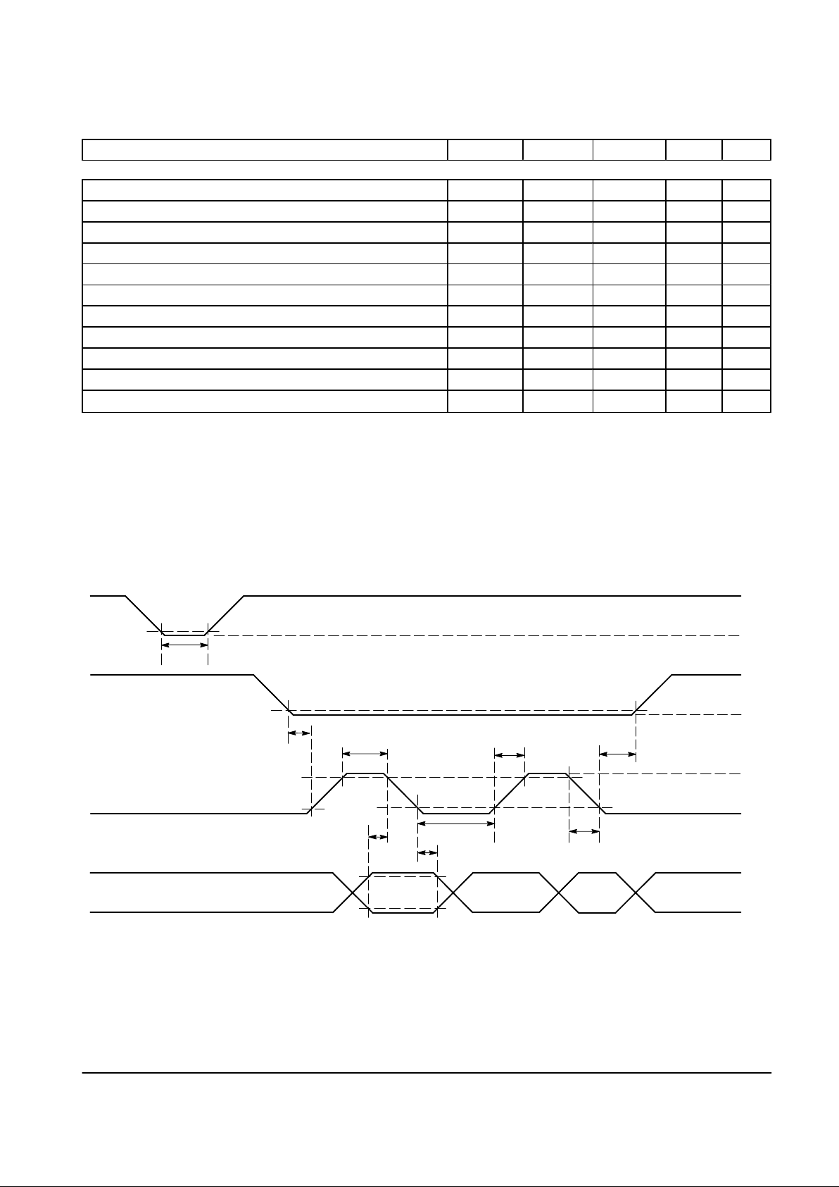
V
IH
V
IL
Don’t Care
0.2 V
DD
0.7 V
DD
t
lag
t
r
t
f
SI
t
wSCLKL
t
SI(hold)
t
SISU
Valid
t
wSCLKH
0.7 V
DD
0.2 V
DD
t
lead
SCLK
0.2 V
DD
0.2 V
DD
t
wRSTB
RSTB
CSB
Don’t Care Don’t CareValid
V
IH
V
IL
V
IH
V
IL
V
IH
V
IL
Figure 2. Input Timing Switch Characteristics
Page 6
MC33298
6
MOTOROLA ANALOG IC DEVICE DATA
DYNAMIC ELECTRICAL CHARACTERISTICS
(Characteristics noted under conditions of 4.5 V ≤ VDD ≤ 5.5 V,
9.0 V ≤ V
PWR
≤ 16 V, – 40°C ≤ TC ≤ 125°C, unless otherwise noted.)
Characteristic
Symbol Min Typ Max Unit
POWER OUTPUT TIMING
Output Rise Time (V
PWR
= 13 V, RL = 26 Ω) (Note 1) t
r
0.4 1.5 20 µs
Output Fall Time (V
PWR
= 13 V, RL = 26 Ω) (Note 1) t
f
0.4 2.5 20 µs
Output Turn “On” Delay Time (V
PWR
= 13 V, RL = 26 Ω) (Note 2) t
dly(on)
1.0 5.0 15 µs
Output Turn “Off” Delay Time (V
PWR
= 13 V, RL = 26 Ω) (Note 3) t
dly(off)
1.0 5.0 15 µs
Output Short Fault Disable Report Delay (Note 4) t
dly(sf)
µs
SFPD = 0.2 x V
DD
25 50 100
Output “Off” Fault Report Delay (Note 5) t
dly(off)
µs
SFPD = 0.2 x V
DD
25 50 100
NOTES: 1. Output Rise and Fall time respectively measured across a 26 Ω resistive load at 10% to 90% and 90% to 10% voltage points.
2.Output Turn “On” Delay time measured from rising edge of CSB to 50% of output “off” V
out
voltage with RL = 26 Ω resistive load
(see Figure 7 and 9).
3.Output Turn “Off” Delay time measured from rising edge of CSB to 50% of output “off” V
out
voltage with RL = 26 Ω resistive load
(see Figure 7 and 9).
4.Output Short Fault Disable Report Delay measured from rising edge of CSB to I
out
= 2.0 A point with output “on,” V
out
= 5.0 V,
and SFPD = 0.2 x VDD (see Figure 8 and 10).
5.Output “Off” Fault Report Delay measured from 50% points of rising edge of CSB to rising edge of output (see Figure 9).
DYNAMIC ELECTRICAL CHARACTERISTICS (Characteristics noted under conditions of 4.5 V ≤ V
DD
≤ 5.5 V,
9.0 V ≤ V
PWR
≤ 16 V , –40°C ≤ TC ≤ 125°C, unless otherwise noted.)
Characteristic Symbol Min Typ Max Unit
DIGITAL INTERFACE TIMING
SCLK Clock Period (Note 6) t
pSCLK
500 – – ns
SCLK Clock High Time t
wSCLKH
175 – – ns
SCLK Clock Low Time t
wSCLKL
175 – – ns
Required Low State Duration for Reset (VIL ≤ 0.2 VDD) (Note 1) t
wRSTB
250 50 – ns
Falling Edge of CSB to Rising Edge of SCLK (Required Setup Time) t
lead
250 50 – ns
Falling Edge of SCLK to Rising Edge of CSB (Required Setup Time) t
lag
250 50 – ns
SI to Falling Edge of SCLK (Required Setup Time) t
SISU
125 25 – ns
Falling Edge of SCLK to SI (Required Hold Time) t
SI(hold)
125 25 – ns
SO Rise Time (CL = 200 pF) t
rSO
– 25 75 ns
SO Fall Time (CL = 200 pF) t
fSO
– 25 75 ns
SI, CSB, SCLK Incoming Signal Rise Time (Note 2) t
rSI
– – 200 ns
SI, CSB, SCLK Incoming Signal Fall TIme (Note 2) t
fSI
– – 200 ns
Time from Falling Edge of CSB to SO ns
Low Impedance (Note 3) t
SO(en)
– – 200
HIgh Impedance (Note 4) t
SO(dis)
– – 200
Time from Rising Edge of SCLK to SO Data Valid (Note 5) t
valid
0.2 VDD ≤ SO ≥ 0.8 VDD, CL = 200 pF – 50 125 ns
NOTES: 1. Reset Low duration measured with outputs enabled and going to “off” or disabled condition.
2. Rise and Fall time of incoming SI, CSB, and SCLK signals suggested for design consideration to prevent the occurrence of double pulsing.
3.Time required for output status data to be available for use at SO.
4.Time required for output status data to be terminated at SO.
5.Time required to obtain valid data out from SO following the rise of SCLK.
6.Clock period includes 75 ns rise plus 75 ns fall transition time in addition to clock high and low time.
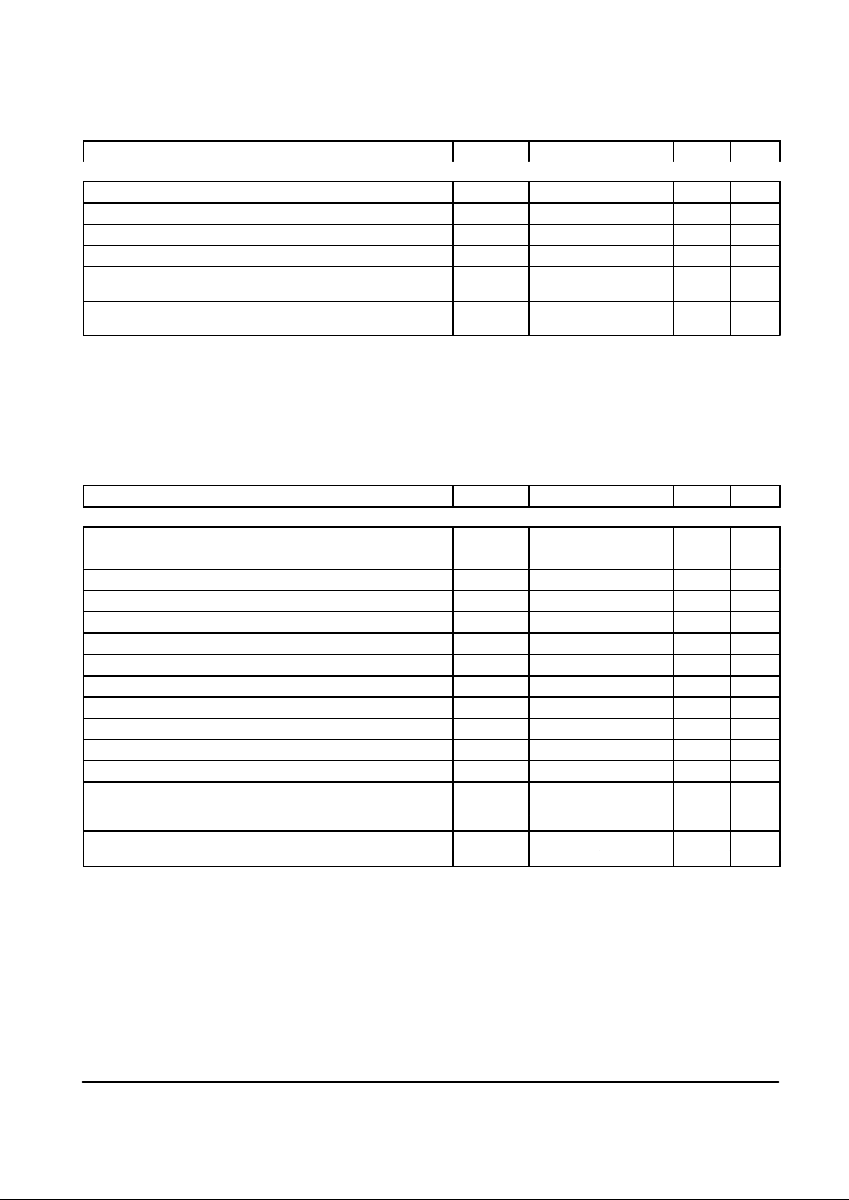
Page 7
MC33298
7
MOTOROLA ANALOG IC DEVICE DATA
(Low–to–High)
SO
CL = 200 pF
VDD = 5.0 V
SCLK
MC33298
Under
Test
CL represents the total capacitance of the test fixture and probe.
t
fSI
t
rSI
0.2 V
DD
0.7 V
DD
0.2 V
DD
0.7 V
DD
t
fSO
t
valid
t
rSO
V
OL
V
OH
V
OL
V
OH
t
dly(hl)
t
dly(lh)
0.2 V
DD
0.7 VDD (2.5 V)
0
5.0 V
≤
10 ns
50%
≤
10 ns
SO (low–to–high) is for an output with internal conditions such that
the low–to–high transition of CSB causes the SO output to switch
from high–to–low.
SO
CL = 20 pF
RL = 2.0 k
Ω
V
Pull–Up
= 2.5 V
VDD = 5.0 V
CSB
MC33298
Under
Test
CL represents the total capacitance of the test fixture and probe.
t
rSI
t
fSI
V
OL
V
OH
V
OL
V
OH
0
5.0 V
SO
t
SO(dis)
t
SO(en)
t
SO(dis)
t
SO(en)
(High–to–Low)
0.7 V
DD
0.2 VDD (2.5 V)
≤
10 ns
≤
10 ns
CSB
NOTES: 1. SO (high–to–low) waveform is for SO output with internal
conditions such that SO output is low except when an output is
disabled as a result of detecting a circuit fault with CSB in a
High Logic state (e.g., open load).
2.SO (low–to–high) waveform is for SO output with internal
conditions such that SO output is high except when an output
is disabled as a result of detecting a circuit fault with CSB in
a High Logic state (e.g., shorted load).
50%
50%
90%
SO
(Low–to–High)
SO
SCLK
(High–to–Low)
SO
50%
10%
Figure 3. Valid Data Delay Time and
Valid Time Test Circuit
Figure 4. Enable and Disable Time Test Circuit
Figure 5. Vaild Data Delay Time and
Valid Time Waveforms
Figure 6. Enable and Disable Time Waveforms
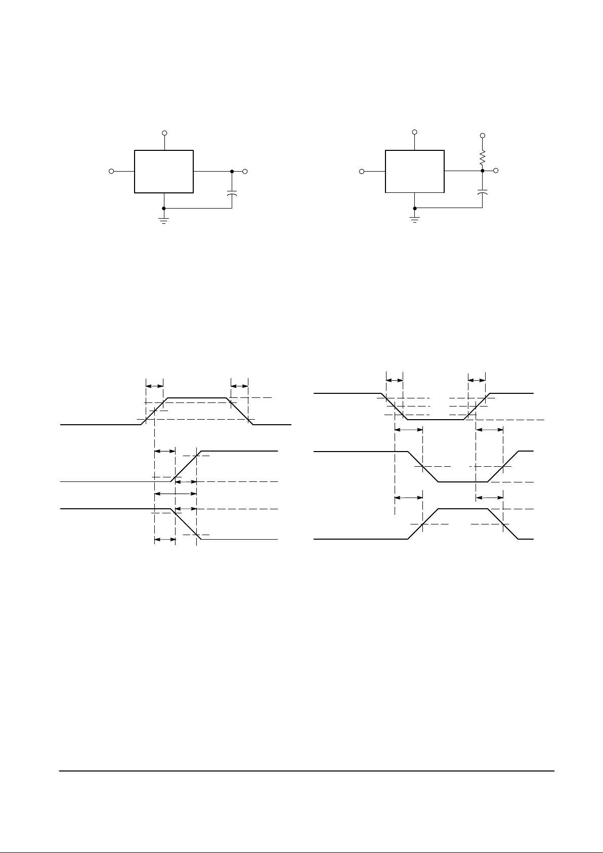
Page 8
MC33298
8
MOTOROLA ANALOG IC DEVICE DATA
Output
C
L
RL = 26
Ω
V
PWR
= 14 V
VDD = 5.0 V
CSB
MC33298
Under
Test
CL represents the total capacitance of the test fixture and probe.
t
fSI
t
rSI
V
OL
14 V
V
OL
14 V
0
5.0 V
t
dly(on)
50%
Output Voltage
Waveform 2
≤
10 ns
50% 10%
90%
≤
10 ns
90%
50%
10%
CSB
t
dly(off)
50%
Output Voltage
Waveform 1
NOTES: 1. t
dly(on)
and t
dly(off)
are turn–on and turn–off propagation
delay times.
2.Waveform 1 is an output programmed from an “on” to an
“off” state.
3. Waveform 2 is an output programmed from an “off” to an
“on” state.
Output
CL = 20 pF
IL = 2.0 A
(Output “On”)
V
PWR
= 11 V
VDD = 5.0 V
CSB
MC33298
Under
Test
CL represents the total capacitance of the test fixture and probe.
t
fSI
t
rSI
0
5.0 V
0
≤
10 ns
≤
10 ns
10%
90%
50%
I
O(CL)
Von = 5.0 V
V
off
= 11 V
Output Current
Waveform
Output Voltage
Waveform
50%
90%
50%
10%
CSB
NOTES: 1. t
pdly(off)
is the output fault unlatch disable propagation delay
time required to correctly report an output fault after CSB rises.
Represents an output commanded “on” while having an existing
output short (overcurrent) to supply.
2. SFPD pin ≤ 0.2 V.
t
dly(off)
Figure 7. Switching Time Test Circuit Figure 8. Output Fault Unlatch Disable
Delay Test Circuit
Figure 9. Turn–On/Off Waveforms Figure 10. Output Fault Unlatch Disable
Delay Waveforms
Page 9

MC33298
9
MOTOROLA ANALOG IC DEVICE DATA
CIRCUIT DESCRIPTION
Introduction
The MC33298 was conceived, specified, designed, and
developed for automotive applications. It is an eight output
low side power switch having 8–bit serial control. The
MC33298 incorporates SMARTMOS technology having
effective 2.0 µ CMOS logic, bipolar/MOS analog circuitry , and
independent state of the art double diffused MOS (DMOS)
power output transistors. Many benefits are realized as a
direct result of using this mixed technology. A simplified block
diagram of the MC33298 is shown in Figure 1.
Where bipolar devices require considerable control
current for their operation, structured MOS devices, since
they are voltage controlled, require only transient gate
charging current affording a significant decrease in power
consumption. The CMOS capability of the SMARTMOS
process allows significant amounts of logic to be
economically incorporated into the monolithic design. In
addition, bipolar/MOS analog circuits embedded within the
updrain power DMOS output transistors monitor and provide
fast, independent protection control functions for each
individual output. All outputs have internal 65 V at 0.5 A
independent output voltage clamps to provide fast inductive
turn–off and transient protection.
The MC33298 uses high efficiency updrain power DMOS
output transistors exhibiting very low drain to source “on”
resistance values (R
DS(on)
≤ 0.45 Ω) and dense CMOS
control logic. Operational bias currents of less than 4.0 mA
(1.0 mA typical) with any combination of outputs “on” are the
result of using this mixed technology and would not be
possible with bipolar structures. T o accomplish a comparable
functional feature set using a bipolar structure approach
would result in a device requiring hundreds of milliamperes of
internal bias and control current. This would represent a very
large amount of power to be consumed by the device itself
and not available for load use.
In operation the MC33298 functions as an eight output
serial switch serving as a microcontroller (MCU) bus
expander and buffer with fault management and fault
reporting features. In doing so, the device directly relieves
the MCU of the fault management functions. The MC33298
directly interfaces to an MCU and operates at system clock
serial frequencies in excess of 2.0 MHz using a Synchronous
Peripheral Interface (SPI) for control and diagnostic readout.
Figure 11 shows the basic SPI configuration between an
MCU and one MC33298.
To
Logic
MC33298
Shift Register
Parallel
Ports
Receive
Buffer
MC68HCXX
Microcontroller
CSB
Rese
t
SCLK
SO
SI
MISO
MOSI
Shift Register
Figure 11. SPI Interface with Microcontroller
The circuit can also be used in a variety of other
applications in the computer, telecommunications, and
industrial fields. It is parametrically specified over an input
“battery”/supply range of 9.0 V to 16 V but is designed to
operate over a considerably wider range of 5.5 V to 26.5 V.
The design incorporates the use of Logic Level MOSFETs as
output devices. These MOSFETs are sufficiently turned “on”
with a gate voltage of less than 5.0 V thus eliminating the
need for an internal charge pump. Each output is identically
sized and independent in operation. The efficiency of each
output transistor is such that with as little as 9.0 V supply
(V
PWR
), the maximum R
DS(on)
of an output at room
temperature is 0.45 Ω (0.35 Ω typical) and increases to only
1.0 Ω (0.5 Ω typical) as V
PWR
is decreased to 5.5 V.
All inputs are compatible with 5.0 V CMOS logic levels and
incorporate negative or inverted logic. Whenever an input is
programmed to a logic low state (< 1.0 V) the corresponding
low side switched output being controlled will be active low
and turned “on.” Conversely, whenever an input is
programmed to a logic high state (> 3.0 V), the output being
controlled will be high and turned “off.”
8 Outputs
SO SI
CSB SCLK
MC33298
8 Outputs
SO SI
CSB SCLK
MC33298
8 Outputs
SO SI
CSB SCLK
MC33298
8 Outputs
SO SI
CSB SCLK
MC33298
Parallel Port
MISO
IRQ
SCLK
MOSI
MC68XX
Microcontroller
SPI
Figure 12. MC33298 SPI System Daisy Chain
Page 10

MC33298
10
MOTOROLA ANALOG IC DEVICE DATA
One main advantage of the MC33298 is the serial port
which when coupled to an MCU, receives “on”/“off”
commands from the MCU and in return transmits the drain
status of the device’s output switches. Many devices can be
“daisy–chained” together to form a larger system (see
Figure 12). Note in this example that only one dedicated
MCU parallel port (aside from the required SPI) is needed for
chip select to control 32 possible loads.
Multiple MC33298 devices can also be controlled in a
parallel input fashion using SPI (see Figure 13). This figure
shows a possible 24 loads being controlled by only three
dedicated parallel MCU ports used for chip select.
SI
CSB
SCLK
8 Outputs
SI
CSB
SCLK
8 Outputs
SI
CSB
SCLK
MC33298
8 Outputs
Parallel
Ports
SCLK
MOSI
MC68XX
Microconttoller
SPI
MC33298
MC33298
A0
A1
A2
Figure 13. Parallel Input SPI Control
Figure 14 shows a basic method of controlling multiple
MC33298 devices using two MCUs. A system can have only
one master MCU at any given instant of time and one or more
slave MCUs. The master MCU supplies the system clock
signal (top MCU designated the master); the lower MCU
being the slave. It is possible to have a system with more
than one master but not at the same time. Only when the
master is not communicating can a slave communicate. MCU
master control is switched through the use of the slave select
(SS
) pin of the MCUs. A master will become a slave when it
detects a logic low state on its SS
pin.
These basic examples make the MC33298 very attractive
for applications where a large number of loads need be
controlled efficiently. The popular Synchronous Serial
Peripheral Interface (SPI) protocol is incorporated, to this
end, to communicate efficiently with the MCU.
SPI System Attributes
The SPI system is flexible enough to communicate directly
with numerous standard peripherals and MCUs available
from Motorola and other semiconductor manufacturers. SPI
reduces the number of pins necessary for input/output (I/O)
on the MC33298. It also offers an easy means of expanding
the I/O function using few MCU pins. The SPI system of
communication consists of the MCU transmitting, and in
return, receiving one databit of information per clock cycle.
Databits of information are simultaneously transmitted by
one pin, Microcontroller Out Serial In (MOSI), and received
by another pin, Microcontroller In Serial Out (MISO), of
the MCU.
Some features of SPI are:
• Full Duplex, Three–Wire Synchronous Data Transfer
• Each Microcontroller can be a Master or a Slave
• Provides Write Collision Flag Protection
• Provides End of Message Interrupt Flag
• Four I/Os associated with SPI (MOSI, MISO, SCLK, SS)
The only drawbacks to SPI are that an MCU is required for
efficient operational control and, in contrast to parallel input
control, is slower at performing pulse width modulating
(PWM) functions.
8–Bit
MC33298
CSB
SCLK
SO
SI
8 Outputs
8–Bit
CSB
SCLK
SO
SI
8 Outputs
MC33298
8–Bit
MC33298
CSB
SCLK
SO
SI
8 Outputs
SS
8–Bit
MC68XX
Microcontroller
SPI
(Master)
MOSI
MISO
Parallel
Ports
SCLK
A0
A1
A2
Figure 14. Multiple MCU SPI Control
B0
B1
V
DD
SS
8–Bit
MC68XX
Microcontroller
SPI
(Alternate
Master)
MOSI
MISO
Parallel
Ports
SCLK
A0
A1
A2
B0
B1
V
DD
Page 11

MC33298
11
MOTOROLA ANALOG IC DEVICE DATA
PIN FUNCTION DESCRIPTION
CSB Pin
The system MCU selects the MC33298 to be
communicated with through the use of the CSB pin.
Whenever the pin is in a logic low state, data can be
transferred from the MCU to the MC33298 and vise versa.
Clocked–in data from the MCU is transferred from the
MC33298 shift register and latched into the power outputs on
the rising edge of the CSB signal. On the falling edge of the
CSB signal, drain status information is transferred from the
power outputs and loaded into the device’s shift register. The
CSB pin also controls the output driver of the serial output
pin. Whenever the CSB pin goes to a logic low state, the SO
pin output driver is enabled allowing information to be
transferred from the MC33298 to the MCU. To avoid any
spurious data, it is essential that the high–to–low transition of
the CSB signal occur only when SCLK is in a logic low state.
SCLK Pin
The system clock pin (SCLK) clocks the internal shift
registers of the MC33298. The serial input pin (SI) accepts
data into the input shift register on the falling edge of the
SCLK signal while the serial output pin (SO) shifts data
information out of the shift register on the rising edge of the
SCLK signal. False clocking of the shift register must be
avoided to guarantee validity of data. It is essential that the
SCLK pin be in a logic low state whenever chip select bar pin
(CSB) makes any transition. For this reason, it is
recommended though not necessary, that the SCLK pin be
kept in a low logic state as long as the device is not accessed
(CSB in logic high state). When CSB is in a logic high state,
any signal at the SCLK and SI pin is ignored and SO is
tristated (high impedance). See the Data Transfer Timing
diagram of Figure 16.
SI Pin
This pin is for the input of serial instruction data. SI
information is read in on the falling edge of SCLK. A logic high
state present on this pin when the SCLK signal rises will
program a specific output “off,” and in turn, turns “off” the
specific output on the rising edge of the CSB signal.
Conversely, a logic low state present on the SI pin will
program the output “on,” and in turn, turns “on” the specific
output on the rising edge of the CSB signal. To program the
eight outputs of the MC33298 “on” or “off,” an eight bit serial
stream of data is required to be entered into the SI pin
starting with Output 7, followed by Output 6, Output 5, etc., to
Output 0. For each rise of the SCLK signal, with CSB held in
a logic low state, a databit instruction (“on” or “off”) is loaded
into the shift register per the databit SI state. The shift register
is full after eight bits of information have been entered. To
preserve data integrity, care should be taken to not transition
SI as SCLK transitions from a low to high logic state.
SO Pin
The serial output (SO) pin is the tri–stateable output from
the shift register. The SO pin remains in a high impedance
state until the CSB pin goes to a logic low state. The SO data
reports the drain status, either high or low. The SO pin
changes state on the rising edge of SCLK and reads out on
the falling edge of SCLK. When an output is “off” and not
faulted, the corresponding SO databit is a high state. When
an output is “on,” and there is no fault, the corresponding
databit on the SO pin will be a low logic state. The SI/SO
shifting of data follows a first–in–first–out protocol with both
input and output words transferring the Most Significant Bit
(MSB) first. The SO pin is not affected by the status of the
Reset pin.
Reset Pin
The MC33298 Reset pin is active low and used to clear the
SPI shift register and in doing so sets all output switches “off.”
With the device in a system with an MCU; upon initial system
power up, the MCU holds the Reset pin of the device in a
logic low state ensuring all outputs to be “off” until both the
VDD and V
PWR
pin voltages are adequate for predictable
operation. After the MC33298 is reset, the MCU is ready to
assert system control with all output switches initially “off.” If
the V
PWR
pin of the MC33298 experiences a low voltage,
following normal operation, the MCU should pull the Reset
pin low so as to shutdown the outputs and clear the input data
register. The Reset pin is active low and has an internal
pull–up incorporated to ensure operational predictability
should the external pull–up of the MCU open circuit. The
internal pull–up is only 20 µA to afford safe and easy
interfacing to the MCU. The Reset pin of the MC33298
should be pulled to a logic low state for a duration of at least
250 ns to ensure reliable reset.
A simple power “on” reset delay of the system can be
programmed through the use of an RC network comprised of
a shunt capacitor from the Reset pin to Ground and a resistor
to VDD (See Figure 15). Care should be exercised to ensure
proper discharge of the capacitor so as to not adversely
delay the reset nor damage the MCU should the MCU pull the
Reset line low and yet accomplish initialization for turn “on”
delay . It may be easier to incorporate delay into the software
program and use a parallel port pin of the MCU to control the
MC33298 Reset pin.
Reset
MCU
MC33298
Reset
20
µ
A
V
DD
R
DLY
C
DLY
Figure 15. Power “On” Reset
SFPD Pin
The Short Fault Protect Disable (SFPD) pin is used to
disable the over current latch–off. This feature allows control
of incandescent loads where in–rush currents exceed the
device’s analog current limits. Essentially the SFPD pin
determines whether the MC33298 output(s) will instantly shut
down upon sensing an output short or remain “on” in a
current limiting mode of operation until the output short is
removed or thermal shutdown is reached. If the SFPD pin is
tied to VDD = 5.0 V the MC33298 output(s) will remain “on” in
a current limited mode of operation upon encountering a load
short to supply. If the SFPD pin is grounded, a short circuit
will immediately shut down only the output affected. Other
outputs not having a fault condition will operate normally . The
short circuit operation is addressed in more detail later.
Page 12

MC33298
12
MOTOROLA ANALOG IC DEVICE DATA
Figure 16.
SCLK
SI
SO
CSB
Output 7
Output 0
D0 D1 D2 D3 D4 D5 D6 D7 D8 D9 D10 D11 D12 D13 D14 D15
OD* OD* OD* OD* OD* OD* OD* OD* D0* D1* D2* D3* D4* D5* D6* D7*
Old Data
Old Data
New Data DO7
New Data DO0
NOTES: 1. Reset pin is in a logic high state during the above operation.
2. D0, D1, D2, ..., and D15 relate to the ordered entry of program data into the MC33298 with D0/D8 bits (MSB) corresponding to Output 7 and D7/D15 corresponding to Output 0.
3. D0*, D1*, D2*, ..., and D7* relate to the ordered data out of the MC33298 with D0* bit (MSB) corresponding to Output 7.
4. OD* corresponds to Old Databits.
5. For brevity, only DO7 and DO0 are shown which respectively correspond to Output 7 and Output 0.
Data Transfer Timing (General)
CSB High–to–Low
CSB Low–to–High
SO
SI
SO pin is enabled. Output Status information transferred to Output Shift Register.
Data from the Shift Register is transferred to the Output Power Switches.
Will change state on the rising edge of the SCLK pin signal.
Will accept data on the falling edge of the SCLK pin signal.
Figure 16. Data Transfer Timing
Page 13

MC33298
13
MOTOROLA ANALOG IC DEVICE DATA
Power Consumption
The MC33298P has extremely low power consumption in
both the operating and standby modes. In the standby or
“sleep” mode, with VDD ≤ 2.0 V, the current consumed by the
V
PWR
pin is less than 50 µA. In the operating mode, the
current drawn by the VDD pin is less than 4.0 mA (1.0 mA
typical) while the current drawn at the V
PWR
pin is 2.0 mA
maximum (1.0 mA typical). During normal operation, turning
outputs “on” increases I
PWR
by only 20 µA per output. Each
output experiencing a “soft short” (overcurrent conditions just
under the current limit), adds 0.5 mA to the I
PWR
current.
Paralleling of Outputs
Using MOSFET s as output switches allows the connection
of any combination of outputs together. MOSFETs have an
inherent positive temperature coefficient thermal feedback
which modulates R
DS(on)
providing balanced current sharing
between outputs without destructive operation (bipolar
outputs could not be paralleled in this fashion as thermal
run–away would likely occur). The device can even be
operated with all outputs tied together. This mode of
operation may be desirable in the event the application
requires lower power dissipation or the added capability of
switching higher currents. Performance of parallel operation
results in a corresponding decrease in R
DS(on)
while the
Output Off Open Load Detect Currents and the Output
Current Limits increase correspondingly (by a factor of eight
if all outputs are paralleled). Less than 56 mΩ R
DS(on)
with
current limiting of 24 to 48 A will result if all outputs are
paralleled together. There will be no change in the
Overvoltage detect or the “Off” Output Threshold Voltage
Range. The advantage of paralleling outputs within the same
MC33298 affords the existence of minimal R
DS(on)
and
output clamp voltage variation between outputs. Typically,
the variation of R
DS(on)
between outputs of the same device
is less than is 0.5%. The variation in clamp voltages (which
could affect dynamic current sharing) is less than 5%.
Paralleling outputs from two or more devices is possible but
not recommended. This is because there is no guarantee
that the R
DS(on)
and clamp voltage of the two devices will
match. System level thermal design analysis and verification
should be conducted whenever paralleling outputs.
FAULT LOGIC OPERATION
General
The MCU can perform a parity check of the fault logic
operation by comparing the command 8–bit word to the
status 8–bit word. Assume that after system reset, the MCU
first sends an 8–bit command word, Command Word 1, to the
MC33298. Each output that is to be turned “on” will have its
corresponding databit low. Refer to the Data Transfer Timing
diagram of Figure 16. As this word, Command Word 1, is
being written into the shift register of the MC33298, a status
word is being simultaneously written out and received by the
MCU. However, the word being received by the MCU is the
status of the previous write word to the MC33298, Status
Word 0. If the command word of the MCU is written a second
time (Command Word 2 = Command Word 1), the word
received by the MCU, Status Word 2, is the status of
Command Word 1. The timing diagram shown in Figure 16
depicts this operation. Status Word 2 is then compared with
Command Word 1. The MCU will Exclusive OR Status Word
2 with Command Word 1 to determine if the two words are
identical. If the two words are identical, no faults exist. The
timing between the two write words must be greater than
100 µs to receive proper drain status. The system databus
integrity may be tested by writing two like words to the
MC33298 within a few microseconds of each other.
Initial System Setup Timing
The MCU can monitor two kinds of faults:
(1) Communication errors on the data bus and
(2) Actual faults of the output loads.
After initial system start up or reset, the MCU will write one
word to the MC33298. If the word is repeated within a few
microseconds (say 5) of the first word, the word received by
the MCU, at the end of the repeated word, serves as a
confirmation of data bus integrity (1). At startup, the
MC33298 will take 25 to 100 µs before a repeat of the first
word can give the actual status of the outputs. Therefore, the
first word should be repeated at least 100 µs later to verify the
status of the outputs.
The SO of the MC33298 will indicate any one of four faults.
The four possible faults are Over Temperature, Output Off
Open Fault, Short Fault (overcurrent), and V
PWR
Overvoltage Fault. All of these faults, with the exception of
the Overvoltage Fault, are output specific. Over Temperature
Detect, Output Off Open Detect, and Output Short Detect are
dedicated to each output separately such that the outputs are
independent in operation. A V
PWR
Overvoltage Detect is of a
“global” nature causing all outputs to be turned “off.”
Over Temperature Fault
Patent pending Over Temperature Detect and shutdown
circuits are specifically incorporated for each individual
output. The shutdown that follows an Over Temperature
condition is independent of the system clock or any other
logic signal. Each independent output shuts down at 155°C
to 185°C. When an output shuts down due to an Over
Temperature Fault, no other outputs are affected. The MCU
recognizes the fault since the output was commanded to be
“on” and the status word indicates that it is “off.” A maximum
hysteresis of 20°C ensures an adequate time delay between
output turn “off” and recovery. This avoids a very rapid turn
“on” and turn “off” of the device around the Over Temperature
threshold. When the temperature falls below the recovery
level for the Over Temperature Fault, the device will turn “on”
only if the Command Word during the next write cycle
indicates the output should be turned “on.”
Overvoltage Fault
An Overvoltage condition on the V
PWR
pin will cause the
MC33298 to shut down all outputs until the overvoltage
condition is removed and the device is re–programmed by
the SPI. The overvoltage threshold on the V
PWR
pin is
specified as 28 V to 36 V with 1.0 V typical hysteresis.
Following the overvoltage condition, the next write cycle
sends the SO pin the hexadecimal word $FF (all ones)
indicating all outputs are turned “off.” In this way, potentially
dangerous timing problems are avoided and the MCU reset
Page 14

MC33298
14
MOTOROLA ANALOG IC DEVICE DATA
routine ensures an orderly startup of the loads. The
MC33298 does not detect an overvoltage on the VDD pin.
Other external circuitry, such as the Motorola MC33161
Universal Voltage Monitor, is necessary to accomplish this
function.
Output Off Open Load Fault
An Output Off Open Load Fault is the detection and
reporting of an “open” load when the corresponding output is
disabled (input in a logic high state). To understand the
operation of the Open Load Fault detect circuit, see
Figure 17. The Output Off Open Load Fault is detected by
comparing the drain voltage of the specific MOSFET output
to an internally generated reference. Each output has one
dedicated comparator for this purpose.
MC33298
R
L
V
PWR
MOSFET “Off”
Low = Fault
50
µ
A
V
Thres
0.6 to 0.8 x V
DD
Output
Figure 17. Output “Off” Open Load Detect
An Output Off Open Load Fault is indicated when the
output voltage is less than the Output Threshold Voltage
(V
Thres
) of 0.6 to 0.8 x VDD. Since the MC33298 outputs
function as switches, during normal operation, each
MOSFET output should either be completely turned “on” or
“off.” By design the threshold voltage was selected to be
between the “on” and “off” voltage of the MOSFET. During
normal operation, the “on” state VDS voltage of the MOSFET
is less than the threshold voltage and the “off” state V
DS
voltage is greater than the threshold voltage. This design
approach affords using the same threshold comparator for
Output Open Load Detect in the “off” state and Short Circuit
Detect in the “on” state. See Figure 18 for an understanding
of the Short Circuit Detect circuit. With VDD = 5.0 V, an “off”
state output voltage of less than 3.0 V will be detected as an
Output Off Open Load Fault while voltages greater than 4.0 V
will not be detected as a fault.
The MC33298 has an internal pull–down current source of
50 µA, as shown in Figure 17, between the MOSFET drain
and ground. This prevents the output from floating up to
V
PWR
if there is an open load or internal wirebond failure. The
internal comparator compares the drain voltage with a
reference voltage, V
Thres
(0.6 to 0.8 x VDD). If the output
voltage is less than this reference voltage, the MC33298 will
declare the condition to be an open load fault.
During steady–state operation, the minimum load
resistance (RL) needed to prevent false fault reporting during
normal operation can be found as follows:
V
PWR
= 9.0 V (min)
I
LCO
= 50 µA
V
Thres
(max) = (0.8 x 5.5)V = 4.4 V
Therefore, the load resistance necessary to prevent false
open load fault reporting is (using Ohm’s Law) equal to 92 kΩ
or less.
During output switching, especially with capacitive loads,
a false Output Off Open Load Fault may be triggered. To
prevent this false fault from being reported an internal fault
filter of 25 to 100 µs is incorporated. The duration for which a
false fault may be reported is a function of the load
impedance (RL, CL, LL), R
DS(on)
, and C
out
of the MOSFET as
well as the supply voltage, V
PWR
. The rising edge of CSB
triggers a built in fault delay timer which must time out (25
to 100 µs) before the fault comparator is enabled to detect a
faulted threshold. The circuit automatically returns to normal
operation once the condition causing the Open Load Fault
is removed.
Shorted Load Fault
A shorted load (overcurrent) fault can be caused by any
output being shorted directly to supply, or an output
experiencing a current greater than the current limit.
There are three safety circuits progressively in operation
during load short conditions which afford system protection:
1) The device’s output current is monitored in an analog
fashion using a SENSEFET approach and limited; 2) The
device’s output current limit threshold is sensed by
monitoring the MOSFET drain voltage; and 3) The device’s
output thermal limit is sensed and when attained causes only
the specific faulted output to be latched “off,” allowing
remaining outputs to operate normally. All three protection
mechanisms are incorporated in each output affording robust
independent output operation.
The analog current limit circuit is always active and
monitors the output drain current. An overcurrent condition
causes the gate control circuitry to reduce the gate to source
voltage imposed on the output MOSFET which
re–establishes the load current in compliance with current
limit (3.0 to 6.0 A) range. The time required for the current
limit circuitry to act is less than 20 µs. Therefore, currents
higher than 3.0 to 6.0 A will never be seen for more than 20 µs
(a typical duration is 10 µs). If the current of an output
attempts to exceed the predetermined limit of 3.0 to 6.0 A
(4.0 A nominal), the VDS voltage will exceed the V
Thres
voltage and the overcurrent comparator will be tripped as
shown in Figure 18.
Figure 18. Short Circuit Detect and Analog
Current Limiting Circuit
MC33298
R
L
V
PWR
MOSFET “On”
High = Fault
V
Thres
0.6 to 0.8 x V
DD
Output
Analog
Digital
V
ref
Page 15

MC33298
15
MOTOROLA ANALOG IC DEVICE DATA
The status of SFPD will determine whether the MC33298
will shut down or continue to operate in an analog current
limited mode until either the short circuit is removed or
thermal shutdown is reached.
Grounding the SFPD pin will enable the short fault
protection shutdown circuitry. Consider a load short (output
short to supply) occurring on an output before, during, and
after output turn “on.” When the CSB signal rises to the high
logic state, the corresponding output is turned “on” and a
delay timer activated. The duration of the delay timer is
25 to 100 µs. If the short circuit takes place before the output
is turned “on,” the delay experienced is the entire
25 to 100 µs followed by shutdown. If the short occurs
during the delay time, the shutdown still occurs after the
delay time has elapsed. If the short circuit occurs after the
delay time, shut– down is immediate (within 20 µs after
sensing). The purpose of the delay timer is to prevent false
faults from being reported when switching capacitive loads.
If the SFPD pin is at 5.0 V (or V
DD)
, an output will not be
disabled when overcurrent is detected. The specific output
will, within 5.0 to 10 µs of encountering the short circuit, go
into an analog current limited mode. This feature is especially
useful when switching incandescent lamp loads, where high
in–rush currents experienced during startup last for
10 to 20 ms.
Each output of the MC33298 has its own overcurrent
shutdown circuitry. Over temperature faults and the
overvoltage faults are not affected by the SFPD pin.
Both load current sensing and output voltage sensing are
incorporated for Short Fault detection with actual detection
occurring slightly after the onset of current limit. The current
limit circuitry incorporates a SENSEFET approach to
measure the total drain current. This calls for the current
through a small number of cells in the power MOSFET to be
measured and the result multiplied by a constant to give the
total current. Whereas output shutdown circuitry measures
the drain to source voltage and shuts down if a threshold
(V
Thres
) is exceeded.
Short Fault detection is accomplished by sensing the
output voltage and comparing it to V
Thres
. The lowest V
Thres
requires a voltage of 0.6 times 4.5 V (the minimum V
DD
voltage) or 2.7 V to be sensed. For an enabled output, with
VDD = 5.0 ± 0.5 V, an output voltage in excess of 4.4 V will be
detected as a “short” while voltages less than 2.7 V will not be
detected as “shorts.”
Over Current Recovery
If the SFPD pin is in a high logic state, the circuit returns to
normal operation automatically after the short circuit is
removed (unless thermal shutdown has occurred).
If the SFPD pin is grounded and overcurrent shutdown
occurs; removal of the short circuit will result in the output
remaining “off” until the next write cycle. If the short circuit is
not removed, the output will turn “on” for the delay time
(25 to 100 µs) and then turn “off” for every write cycle
commanding a turn “on.”
SFPD Pin Voltage Selection
Since the voltage condition of the SFPD pin controls the
activation of the short fault protection (i.e. shutdown) mode
equally for all eight outputs, the load having the longest
duration of in–rush current determines what voltage (state)
the SFPD pin should be at. Usually if at least one load is, say
an incandescent lamp, the in–rush current on that input will
be milliseconds in duration. Therefore, setting SFPD at 5.0 V
will prevent shutdown of the output due to the in–rush
current. The system relies only on the Over Temperature
Shutdown to protect the outputs and the loads. The
MC33298 was designed to switch GE194 incandescent
lamps with the SFPD pin in a grounded state. Considerably
larger lamps can be switched with the SFPD pin held in a
high logic state.
Sometimes both a delay period greater than 25 to 100 µs
(current limiting of the output) followed by an immediate over
current shutdown is necessary. This can be accomplished by
programming the SFPD pin to 5.0 V for the extended delay
period to afford the outputs to remain “on” in a current limited
mode and then grounding it to accomplish the immediate
shutdown after some period of time. Additional external
circuitry is required to implement this type of function. An
MCU parallel output port can be devoted to controlling the
SFPD voltage during and after the delay period, is often a
much better method. In either case, care should be taken to
execute the SFPD start–up routine every time start–up or
reset occurs.
Undervoltage Shutdown
An undervoltage VDD condition will result in the global
shutdown of all outputs. The undervoltage threshold is
between 2.5 V and 4.5 V. When VDD goes below the
threshold, all outputs are turned “off” and the SO register is
reset to indicate the same.
An undervoltage condition at the V
PWR
pin will not cause
output shutdown and reset. When V
PWR
is between 5.5 V
and 9.0 V, the outputs will operate per the command word.
However, the status as reported by the serial output (SO) pin
may not be accurate. Proper operation at V
PWR
voltages
below 5.5 V cannot be guaranteed.
Deciphering Fault Type
The MC33298 SO pin can be used to understand what
kind of system fault has occurred. With eight outputs having
open load, over current and over temperature faults, a total of
25 different faults are possible. The SO status word received
by the MCU will be compared with the word sent to the
MC33298 during the previous write cycle. If the two words
are not the same, then the MCU should be programmed to
determine which output or outputs are indicating faults. If the
command bit for any of the output switches indicating a fault
is high, the fault is an open load.
The eight open load faults are therefore the ones most
easily detected. Over current and over temperature faults are
often related. Turning the affected output switches “off” and
waiting for some time should make these faults go away.
Over current and over temperature faults can not be
differentiated in normal application usage.
One advantage of the synchronous serial output is that
multiple faults can be detected with only one pin (SO) being
used for fault status indication.
If V
PWR
experiences an overvoltage condition, all outputs
will immediately be turned “off” and remain latched “off.”
A new command word is required to turn the outputs back
“on” following an overvoltage condition.
Page 16

MC33298
16
MOTOROLA ANALOG IC DEVICE DATA
Output Voltage Clamping
Each output of the MC33298 incorporates an internal
voltage clamp to provide fast turn–off and transient protection
of the output. Each clamp independently limits the drain to
source voltage to 65 V at drain currents of 0.5 A and keeps
the output transistors from avalanching by causing the
transient energy to be dissipated in the linear mode (see
Figure 19). The total energy (EJ) can be calculated by
multiplying the current area under the current curve (IA)
during the time the clamp is active and the clamp
voltage (VCL).
Characterization of the output clamps, using a single pulse
repetitive method at 0.5 A, indicate the maximum energy to
be 100 mJ at 25°C and 25 mJ at 125°C per output. Using a
single pulse non–repetitive method at 0.5 A the clamps are
capable of 2.0 Joules at 25°C and 0.5 Joules at 125°C.
Clamp Energy
(EJ = IA x VCL x t)
Drain Voltage
Time
Current
Area (IA)
Gnd
Drain–to–Source “On”
V
PWR
Drain Current
(ID = 0.5 A)
Drain–to–Source Clamp
Voltage (VCL = 65 V)
Figure 19. Output Voltage Clamping
Voltage (V
DS(ON)
)
THERMAL CHARACTERIZA TION
Thermal Model
Logic functions take up a very small area of the die and
generate negligible power. In contrast, the output transistors
take up most of the die area and are the primary contributors
of power generation. The thermal model shown in Figure 20
was developed for the MC33298 mounted on a typical PC
board. The model is accurate for both steady state and
transient thermal conditions. The components Rd0, Rd1,
R
d2,
..., and Rd7 represent the steady state thermal
resistance of the silicon die for transistor outputs 0, 1, 2, ...,
and 7, while Cd0, Cd1, Cd2, ..., and Cd7 represent
the corresponding thermal capacitance of the silicon
die transistor outputs and plastic. The device area and
die thickness determine the values of these specific
components.
The thermal impedance of the package from the internal
mounting flag to the outside environment is represented by
the terms R
pkg
and C
pkg
. The steady state thermal resistance
of leads and the PC board make up the steady state package
thermal resistance, R
pkg
. The thermal capacitance of the
package is made up of the combined capacitance of the flag
and the PC board. The mold compound was not modeled as
a specific component but is factored into the other overall
component values.
The battery voltage in the thermal model represents the
ambient temperature the device and PC board are subjected
to. The I
PWR
current source represents the total power
dissipation and is calculated by adding up the power
dissipation of each individual output transistor. This is easily
done by knowing R
DS(on)
and load current of the
individual outputs.
Very satisfactory steady state and transient results have
been experienced with this thermal model. Tests indicate the
model accuracy to have less than 10% error. Output
interaction with an adjacent output is thought to be the main
contributor to the thermal inaccuracy. Tests indicate little or
no detectable thermal affects caused by distant output
transistors which are isolated by one or more other outputs.
Tests were conducted with the device mounted on a typical
PC board placed horizontally in a 33 cubic inch still air
enclosure. The PC board was made of FR4 material
measuring 2.5″ by 2.5″, having double–sided circuit traces of
1.0 oz. copper soldered to each device pin. The board
temperature was measured with thermal couple soldered to
the board surface one inch away from the center of the
device. The ambient temperature of the enclosure was
measured with a second thermal couple located over the
center and one inch distant from device.
Thermal Performance
Figure 20 shows the worst case thermal component
parameters values for the MC33298 in the 20 pin plastic
power DIP and the SOP–24 wide body surface mount
package. The power DIP package has Pins 5, 6, 15, and 16
connected directly to the lead frame flag. The parameter
values indicated take into account adjacent output cell thermal
pulling effects as well as different output combinations. The
characterization was conducted over power dissipation levels
of 0.7 to 17 W. The junction–to–ambient temperature thermal
resistance was found to be 37°C/W with a single output
active (31°C/W with all outputs dissipating equal power) and
in conjunction with this, the thermal resistance from junction
to PC board (R
junction–board
) was found to be 27°C/W (board
temperature, measured 1″ from device center). In addition,
the thermal resistance from junction–to–heatsink lead was
found to approximate 10°C/W. Devoting additional PC board
metal around the heatsinking pins improved R
pkg
from 30° to
28°C/W.
The SOP–24 package has Pins 5, 6, 7, 8, 17, 18, 19, and
20 of the package connected directly to the lead frame flag.
Characterization was conducted in the same manner as for
the DIP package. The junction–to–ambient temperature
resistance was found to be 40°C/W with a single output
active (34°C/W with all outputs dissipating equal power) and
the thermal resistance from junction–to–PC board
(R
junction–board
) to be 30°C/W (board temperature,
measured 1″ from device center). The junction–to–heatsink
lead resistance was found again to approximate 10°C/W.
Devoting additional PC board metal around the heatsinking
pins for this package improved the R
pkg
from 33° to 31°C/W.
The total power dissipation available is dependent on the
number of outputs enabled at any one time. At 25°C the
R
DS(on)
is 450 mΩ with a coefficient of 6500 ppm/°C. For the
junction temperature to remain below 150°C, the maximum
available power dissipation must decrease as the ambient
temperature increases. Figures 21 and 22 depict the per
output limit of current at ambient temperatures necessary for
the plastic DIP and SOP packages respectively when one,
four, or eight outputs are enabled “on.” Figure 23 depicts how
the R
DS(on)
output value is affected by junction temperature.
Page 17

MC33298
17
MOTOROLA ANALOG IC DEVICE DATA
*Ω = °C/W, F = W s/°C, I
PWR
= W, and VA = °C
0.15
0.2
C
pkg
(F)*
33
30
R
pkg
(Ω)*
0.002
0.002
C
dx
(F)*
7.0
7.0
R
dx
(Ω)*
SOP–24L
20 Pin DIP
Package
Output 7Output 6Output 2Output 1Output 0
I
PWR
(Steady State or Transient)
(1.0 A = 1.0 W of Device Power Dissipation)
Junction Temperature Node
VD = TD (
°
C)
(Volts represent Die Surface Temperature)
Ambient Temperature Node
VA = TA (
°
C)
(1.0 V = 1
°
C Ambient Temperature)
Flag Temperature Node
C
pkg
= C
flag
+ CPC
Board
R
pkg
= R
leads
+ RPC
Board
C
d7
R
d7
C
d6
R
d6
C
d2
R
d2
C
d1
R
d1
C
d0
R
d0
Figure 20. Thermal Model (Electrical Equivalent)
Page 18

MC33298
18
MOTOROLA ANALOG IC DEVICE DATA
1 Output “On” (40°C/W)
1 Output “On” (37°C/W)
8 Outputs “On” (31°C/W)
4 Outputs “On” (32°C/W)
4 Outputs “On” (35°C/W)
I
L(max)
, , MAXIMUM CURRENT PER OUTPUT (A)
I
L(max)
, , MAXIMUM CURRENT PER OUTPUT (A)
Figure 21. Maximum DIP Package Steady State
Output Current versus Ambient Temperature
–50
TA, AMBIENT TEMPERATURE (
°
C)
Figure 22. Maximum SOP Package Steady State
Ouput Current versus Ambient Temperature
3.0
–50
TA, AMBIENT TEMPERATURE (
°
C)
2.5
2.0
1.5
1.0
0.5
0
– 25 0 25 50 75 100 125 150
– 25 0 25 50 75 100 125 150
2.5
2.0
1.5
1.0
0
0.5
8 Outputs “On” (34°C/W)
R
DS(on)
, OUTPUT “ON” RESISTANCE ( )
Ω
–50
0.9
TJ, JUNCTION TEMPERATURE (
°
C)
Figure 23. Maximum Output “On” Resistance
versus Junction Temperature
0.7
0.6
0.5
0.4
0.2
0.3
– 25 0 25 50 75 100 125 150
0.8
R
DS(on)
@ 150°C = 0.8
Ω
TJ = 150°C
R
DS(on)
@ 150°C = 0.8
Ω
TJ = 150°C
V
PWR
= 13 V
VDD = 5.0 V
I
OUT
= 0.5 A
Page 19

MC33298
19
MOTOROLA ANALOG IC DEVICE DATA
Latch–Up Immunity
Device latch–up caused by substrate injection has been
characterized. Latch–up immunity has both a dc and a
transient immunity component. DC latch–up immunity results
indicate the device to be capable of withstanding in excess of
four amps of reverse current out of any of the output
transistors while the control logic continues to function
normally. The logic control current (IDD) was found to
increase by only 0.6 mA with four amps of current being
pulled out of an output. Additionally, the I
PWR
current was
found to increase by only 0.15 mA under the same condition.
These increases are a result of minority carriers being
injected into substrate and subsequently being collected.
The following procedure has been developed to test for
transient latch–up immunity and has been applied to this
automotive circuit design. Results of transient testing indicate
the device to operate properly at output currents greater than
1.5 A. The procedure tests for the device’s immunity to
intermittent load to battery current connection with the device
controlling an inductive load. Appropriately termed “the file
test,” the battery is connected to a shop file while the lead to
the inductive load is dragged across the files surface causing
intermittent load opens producing lots of arcs, sparks, and
smoke, plus severe transients (see Figure 24). It is during
these severe transients that latch–up most likely could occur.
The battery voltage used for this test was 18 V and the
inductive load was 2.0 mH. These values were found to
produce severe transient stresses of the device outputs. All
outputs must maintain operation and input control during
transient generation to pass “the file test.”
The device’s input control currents were found to remain
stable and were not affected by dc or transient latch–up
immunity testing.
Figure 24. Transient Latch–Up Immunity File Test
Battery
0.1 µF
I
limit
Output 0
R
S
Open
Load
Detect
Short
Circuit
Detect
Over
T emperature
Detect
SO
SI
SCLK
CSB
Reset
SFPD
V
DD
Gate
Control
65 V
Outputs
1–7
Grounds
V
PWR
APPLICATIONS INFORMATION
SIOP Communication
Two common communication protocols used in Motorola’s
microprocessors are the Serial Peripheral Interface (SPI) and
Synchronous Input Output Port (SIOP). SIOP is a subset of
the more flexible SPI and the simpler of the two protocols.
SIOP is used on many of the MC68HC05 family of
microcontrollers. Restrictions of the SIOP protocol include:
1) the SCLK frequency is fixed at one–fourth the internal
clock rate and 2) the polarity of the SCLK signal is fixed.
By way of example, the MC68HC05P9 utilizes SIOP
protocol and is not directly compatible with the serial input
requirements of the MC33298. Specifically, the MC33298
accepts data on the falling edge of SCLK whereas its rising
edge triggers data transfer in the SIOP protocol. SCLK is high
during SIOP transmissions, which is the opposite of what the
MC33298 requires.
Though designed specifically for SPI communication
protocol, the MC33298 can easily be adapted to
communicate with SIOP protocol through the use of
software. The amount of code required to implement SPI in
software is relatively small, so the only major drawback is a
slower transfer of data. The software routine shown in
Table 1 completes a transfer in about 100 µs.
Cost
The bottom line relates to cost. The MC33298 is a very
cost effective octal output serial switch for applications
typically encountered in the automotive and industrial market
segments. To accomplish only the most basic serial switch
function the MC33298 offers, using a discrete semiconductor
approach, would require the use of at least eight logic level
power MOSFETs for the outputs and two shift registers for
the I/O plus other miscellaneous “glue” components.
Additional circuitry would have to be incorporated to
accomplish the protection features offered by the MC33298.
Other noteworthy advantages the MC33298 offers are
conservation of power and board space, requirement of
fewer application components, and enhanced application
reliability. The MC33298 is available at a fraction of the cost
required for discrete component implementation and
represents true value.
The MC33298 represents a cost effective device having
advanced performance and features and worthy of
consideration.
Page 20

MC33298
20
MOTOROLA ANALOG IC DEVICE DATA
Table 1. Program to Exercise the MC33298 Using SPI (Having Only SIOP) Protocol
SET LABELS FOR OUTPUT REGISTERS
PORTA
EQU $0000 ;SPI Port
;DO (Data Out), SCLK, CS, RESET, X, FLTOUT, DI (Data In)
PORTB EQU $0001 ;Normally the SIOP Port. SIOP will be disabled
PORTC EQU $0002 ;A–D Converter Port
PORTD EQU $0003 ;Timer Capture Port
DDRA EQU $0004 ;Data Direction Register for SPI Port
DDRB EQU $0005 ;Data Direction Register for SCLK, SDI, SDO, 11111
DDRC EQU $0006 ;Data Direction Register for A–D Converter Port
DDRD EQU $0007 ;Data Direction Register for PORTD, Timer Capture
DTOUT EQU $0080 ;Register for the SPI output data. This register will be used for a Serial–to–Parallel transformation.
DATAIN EQU $0081 ;Input Register for SPI. Also used for a Serial–to–Parallel transformation.
VALUE EQU $0082 ;Register to store the SPI. Also used for a Serial–to–Parallel transformation.
DATA1 EQU $0083 ;Miscellaneous data register
SCR EQU $000A ;Label for SIOP control register, 0 SPE 0 MSTR 0 0 0 0.
SSR EQU $000B ;Label for SIOP status register, SPIF DCOL 0 0 0 0 0 0, Read Only Register.
SDR EQU $000C ;Label for SIOP data register.
ORG $0100 ;Program starts at first byte of User ROM.
INIT RSP ;Reset Stack Pointer to $FF.
INITIALIZE THE DATA REGISTERS AND THEIR DATA DIRECTION BIT REGISTERS
LDA #$FE ;Configuration PortA as the SPI Port.
STA DDRA ;All but Bit 0 will be outputs.
LDA #$FF
STA DDRB ;Configure Register B as an output. SIOP is not used for the MC33298, but is available for
another peripheral.
STA DDRC ;Configure Register C as an output
STA DDRD ;Configure Register D as an output
LDA #%00010000 ;Initialize the SIOP Control Register.
STA SCR ;Disable SIOP by clearing Bit 6.
SELECT THE DESIRED OUTPUTS
TOP LDA
STA
#$55
VALUE
Select outputs of MC33298 to be turned “on.” This instruction is left inside the loop to include
changes while running the program. A set bit will cause the associated MC33298 output to be
“off.” The value register is uncorrupted by the serial–to–parallel conversion.
BSET 4,PORTA ;Reset the MC33298.
BCLR 4,PORT A ;Also establishes a + or – trigger source
BSET 4,PORTA ;The MC33298 is reset with a logic low.
BCLR 5,PORTA ;Enable MC33298 by pulling CSB (chip select bar) low. Within the MC33298 the Fault Status is
transferred to the MC33298 Serial Register at a falling edge of CSB.
LDA VALUE ;Select outputs to be turned “on.”
STA DT OUT ;Save Output Word (Value) to check for fault.
Page 21

MC33298
21
MOTOROLA ANALOG IC DEVICE DATA
SPI TRANSFER LOOP
LDX #$07 ;Set the number of Read/Shift cycles.
LOOP ASL DATAIN ;Shift a Zero into LSB of DATAIN and ASL other bits.
ASL DTOUT ;Test value currently in MSB of DTOUT.
BCS DOONE ;
BCLR 7,PORTA ;MSB was Zero, so clear DA TA OUT bit.
JMP GOON
DOONE BSET 7,PORTA ;MSB was One, so set the DATA OUT bit.
GOON BSET 6,PORTA ;Set the SCLK. Serial Output pin of the MC33298 changes state on the rising edge of the SCLK.
Read the next bit coming from the MC33298.
BRCLR 0,PORTA,
WZZER0
;Read the bit and branch if Zero. LSB of DATAIN is already cleared due to the ASL above.
BSET 0,DATAIN ;Bit was One. Set the next bit in DATAIN.
WZZER0 BCLR 6,PORTA ;Clear SCLK. Falling edge causes the MC33298 to read the next bit from the MCU.
DECX
BPL LOOP ;Continue to loop eight times until the SPI transfer is complete.
BSET 5,PORTA ;Transfer control signal to output transistors.
ESTABLISH A BRIEF DELAY
LDA #16
PAUSE DECA ;3 Clock cycles
BNE PAUSE ;3 Clock cycles
BCLR 5,PORTA ;Transfer output status to Serial Register.
JSR FLTCHK ;Jump to Fault Check subroutine.
JSR DLY ;Delay 1/T msec
BSET 5,PORTA ;Deselect the MC33298.
BRA TOP ;Return to top of loop.
SUBROUTINE TO CHECK FOR FAULTS
FLTCHK BCLR 1,PORTA ;CLR the Fault pin.
LDA DATAIN
CMP VALUE ;Check for Faults.
BEQ NOFLT ;If there is no Fault, continue.
BSET 1,PORTA ;Activate Fault LED.
NOFLT RTS
Page 22

MC33298
22
MOTOROLA ANALOG IC DEVICE DATA
DELAY SUBROUTINE
DLY
STA DATA1 ;Save Accumulator in RAM.
LDA #$04 ;Do outer loop 4 times, roughly 4.0 ms.
OUTLP CLRX ;X used as Inner Loop Count
INNRLP DECX ;0–FF, FF–FE, … 1–0 256 loops.
BNE INNRLP ;6CYC* 256* 1.0 µs/CYC = 1.53 ms
DECA ;4–3. 3–2, 2–1, 1–0
BNE OUTLP ;1545CYC* 4*1.0 µs/CYC = 6.18 ms
LDA DATA1 ;Recover Accumulator value.
RTS ;Return from subroutine.
ORG $1FF
FDB INIT
Page 23

MC33298
23
MOTOROLA ANALOG IC DEVICE DATA
P SUFFIX
PLASTIC PACKAGE
CASE 738–03
DIP (16+2+2)
ISSUE E
DW SUFFIX
PLASTIC PACKAGE
CASE 751E–04
SOP (16+4+4)L
ISSUE E
OUTLINE DIMENSIONS
1.070
0.260
0.180
0.022
0.070
0.015
0.140
15
°
0.040
1.010
0.240
0.150
0.015
0.050
0.008
0.110
0
°
0.020
25.66
6.10
3.81
0.39
1.27
0.21
2.80
0
°
0.51
27.17
6.60
4.57
0.55
1.77
0.38
3.55
15
°
1.01
0.050 BSC
0.100 BSC
0.300 BSC
1.27 BSC
2.54 BSC
7.62 BSC
MIN MINMAX MAX
INCHES MILLIMETERS
DIM
A
B
C
D
E
F
G
J
K
L
M
N
NOTES:
1. DIMENSIONING AND TOLERANCING PER ANSI
Y14.5M, 1982.
2. CONTROLLING DIMENSION: INCH.
3. DIMENSION L TO CENTER OF LEAD WHEN
FORMED PARALLEL.
4. DIMENSION B DOES NOT INCLUDE MOLD
FLASH.
–A
–
C
K
N
E
GF
D
20 PL
J 20 PL
L
M
–T
–
SEATING
PLANE
110
1120
0.25 (0.010) T A
M M
0.25 (0.010) T B
M M
B
NOTES:
1. DIMENSIONING AND TOLERANCING PER ANSI
Y14.5M, 1982.
2. CONTROLLING DIMENSION: MILLIMETER.
3. DIMENSIONS A AND B DO NOT INCLUDE
MOLD PROTRUSION.
4. MAXIMUM MOLD PROTRUSION 0.15 (0.006)
PER SIDE.
5. DIMENSION D DOES NOT INCLUDE DAMBAR
PROTRUSION. ALLOWABLE DAMBAR
PROTRUSION SHALL BE 0.13 (0.005) TOTAL IN
EXCESS OF D DIMENSION AT MAXIMUM
MATERIAL CONDITION.
–A–
–B– P12X
D24X
12
1324
1
M
0.010 (0.25) B
M
S
A
M
0.010 (0.25) B
S
T
–T–
G
22X
SEATING
PLANE
K
C
R
X 45
_
M
F
J
DIM MIN MAX MIN MAX
INCHESMILLIMETERS
A 15.25 15.54 0.601 0.612
B 7.40 7.60 0.292 0.299
C 2.35 2.65 0.093 0.104
D 0.35 0.49 0.014 0.019
F 0.41 0.90 0.016 0.035
G 1.27 BSC 0.050 BSC
J 0.23 0.32 0.009 0.013
K 0.13 0.29 0.005 0.011
M 0 8 0 8
P 10.05 10.55 0.395 0.415
R 0.25 0.75 0.010 0.029
____
Page 24

MC33298
24
MOTOROLA ANALOG IC DEVICE DATA
Motorola reserves the right to make changes without further notice to any products herein. Motorola makes no warranty , representation or guarantee regarding
the suitability of its products for any particular purpose, nor does Motorola assume any liability arising out of the application or use of any product or circuit, and
specifically disclaims any and all liability, including without limitation consequential or incidental damages. “T ypical” parameters which may be provided in Motorola
data sheets and/or specifications can and do vary in different applications and actual performance may vary over time. All operating parameters, including “Typicals”
must be validated for each customer application by customer’s technical experts. Motorola does not convey any license under its patent rights nor the rights of
others. Motorola products are not designed, intended, or authorized for use as components in systems intended for surgical implant into the body, or other
applications intended to support or sustain life, or for any other application in which the failure of the Motorola product could create a situation where personal injury
or death may occur. Should Buyer purchase or use Motorola products for any such unintended or unauthorized application, Buyer shall indemnify and hold Motorola
and its officers, employees, subsidiaries, affiliates, and distributors harmless against all claims, costs, damages, and expenses, and reasonable attorney fees
arising out of, directly or indirectly, any claim of personal injury or death associated with such unintended or unauthorized use, even if such claim alleges that
Motorola was negligent regarding the design or manufacture of the part. Motorola and are registered trademarks of Motorola, Inc. Motorola, Inc. is an Equal
Opportunity/Affirmative Action Employer.
How to reach us:
USA/EUROPE /Locations Not Listed: Motorola Literature Distribution; JAPAN: Nippon Motorola Ltd.; Tatsumi–SPD–JLDC, 6F Seibu–Butsuryu–Center,
P.O. Box 20912; Phoenix, Arizona 85036. 1–800–441–2447 or 602–303–5454 3–14–2 Tatsumi Koto–Ku, Tokyo 135, Japan. 03–81–3521–8315
MFAX: RMF AX0@email.sps.mot.com – TOUCHT ONE 602–244–6609 ASIA/PACIFIC: Motorola Semiconductors H.K. Ltd.; 8B Tai Ping Industrial Park,
INTERNET: http://Design–NET.com 51 Ting K o k Road, Tai Po, N.T ., Hong Kong. 852–26629298
MC33298/D
*MC33298/D*
◊
 Loading...