

Datasheet MC33263NW-28R2, MC33263NW-30R2, MC33263NW-38R2, MC33263NW-40R2, MC33263NW-47R2 Datasheet (MOTOROLA)
...Page 1
MC33263
Ultra Low Noise
150 mA Low Dropout
Voltage Regulator with
ON/OFF Control
Housed in a SOT23–L package, the MC33263 delivers up to
150 mA where it exhibits a typical 180 mV dropout. With an
incredible noise level of 25 mVRMS (over 100 Hz to 100 kHz, with a
10 nF bypass capacitor), the MC33263 represents the ideal choice for
sensitive circuits, especially in portable applications where noise
performance and space are premium. The MC33263 also excels in
response time and reacts in less than 25 ms when receiving an OFF to
ON signal (with no bypass capacitor).
Thanks to a novel concept, the MC33263 accepts output capacitors
without any restrictions regarding their Equivalent Series Resistance
(ESR) thus offering an obvious versatility for immediate implementation.
With a typical DC ripple rejection better than –90 dB (–70 dB @
1 kHz), it naturally shields the downstream electronics against choppy
power lines.
Additionally, thermal shutdown and short–circuit protection
provide the final product with a high degree of ruggedness.
Features:
• Very Low Quiescent Current 170 µA (ON, no load), 100 nA (OFF,
no load)
• Very Low Dropout Voltage, typical value is 137 mV at an output
current of 100 mA
• Very Low Noise with external bypass capacitor (10 nF),
typically 25 µV rms over 100 Hz to 100 kHz
• Internal Thermal Shutdown
• Extremely Tight Line Regulation typically –90 dB
• Ripple Rejection –70 dB @ 1 kHz
• Line Transient Response: 1 mV for
• Extremely Tight Load Regulation, typically 20 mV at
• Multiple Output Voltages Available
• Logic Level ON/OFF Control (TTL–CMOS Compatible)
• ESR can vary from 0 to 3
W
• Functionally and Pin Compatible with TK112xxA/B Series
Applications:
• All Portable Systems, Battery Powered Systems, Cellular
T elephones, Radio Control Systems, Toys and Low Voltage Systems
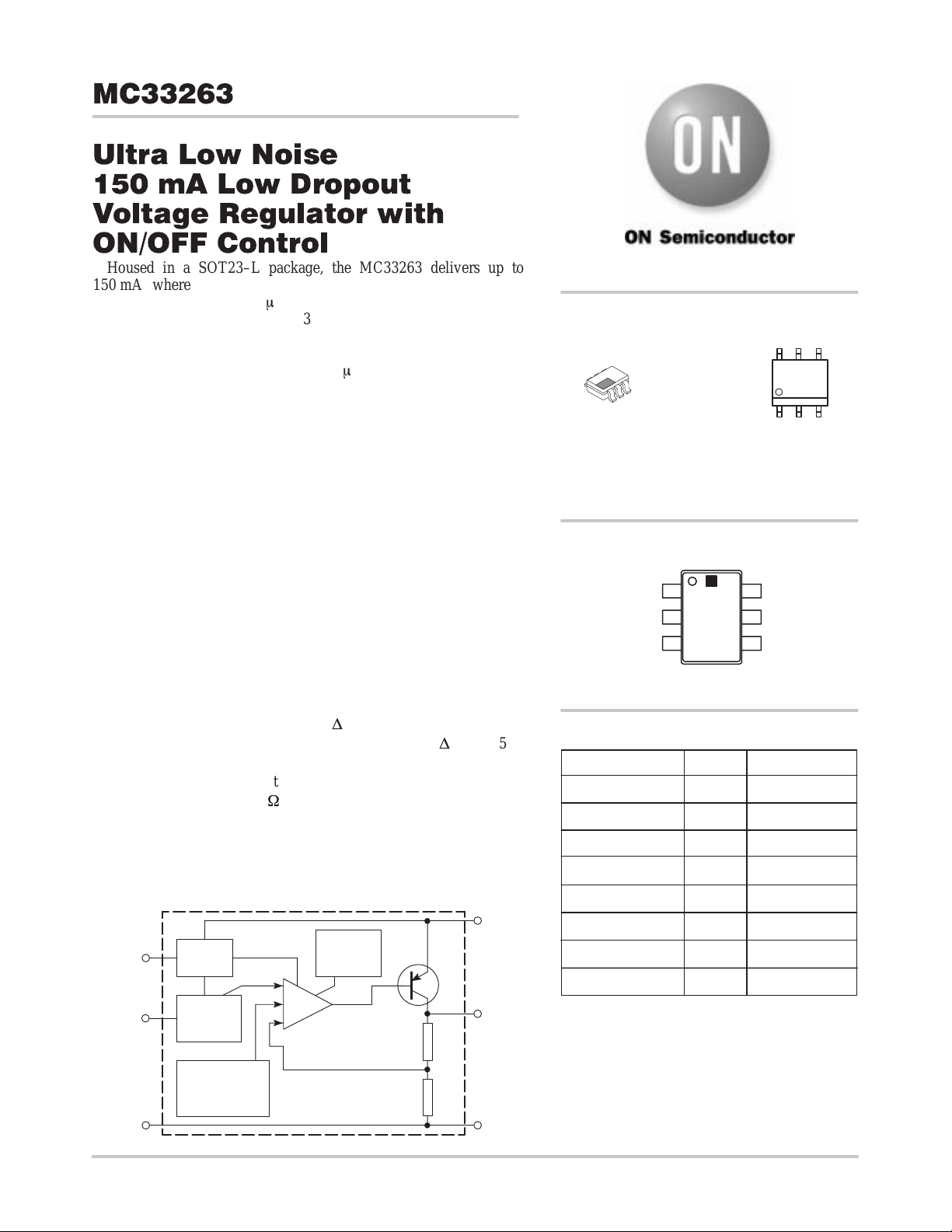
MC33263 Block Diagram
Bypass
1
ON/OFF
3
Band Gap
Reference
Shutdown
D
Vin = 3 V
Thermal
Shutdown
D
I
out
= 150 mA
6
Input
4
Output
http://onsemi.com
MARKING
DIAGRAMS
6
SOT–23L
6
1
Device Version Shipping
MC33263NW–28R2 2.8 V 2500 Tape & Reel
MC33263NW–30R2 3.0 V 2500 Tape & Reel
MC33263NW–32R2 3.2 V
MC33263NW–33R2 3.3 V
MC33263NW–38R2 3.8 V 2500 Tape & Reel
MC33263NW–40R2 4.0 V 2500 Tape & Reel
MC33263NW–47R2 4.75 V 2500 Tape & Reel
MC33263NW–50R2 5.0 V 2500 Tape & Reel
All Devices Available in SOT–23L 6 Lead Package
NW SUFFIX
CASE 318J
x = Voltage Option Code
A = Assembly Location
WL, L = Wafer Lot
YY, Y = Year
WW, W= Work Week
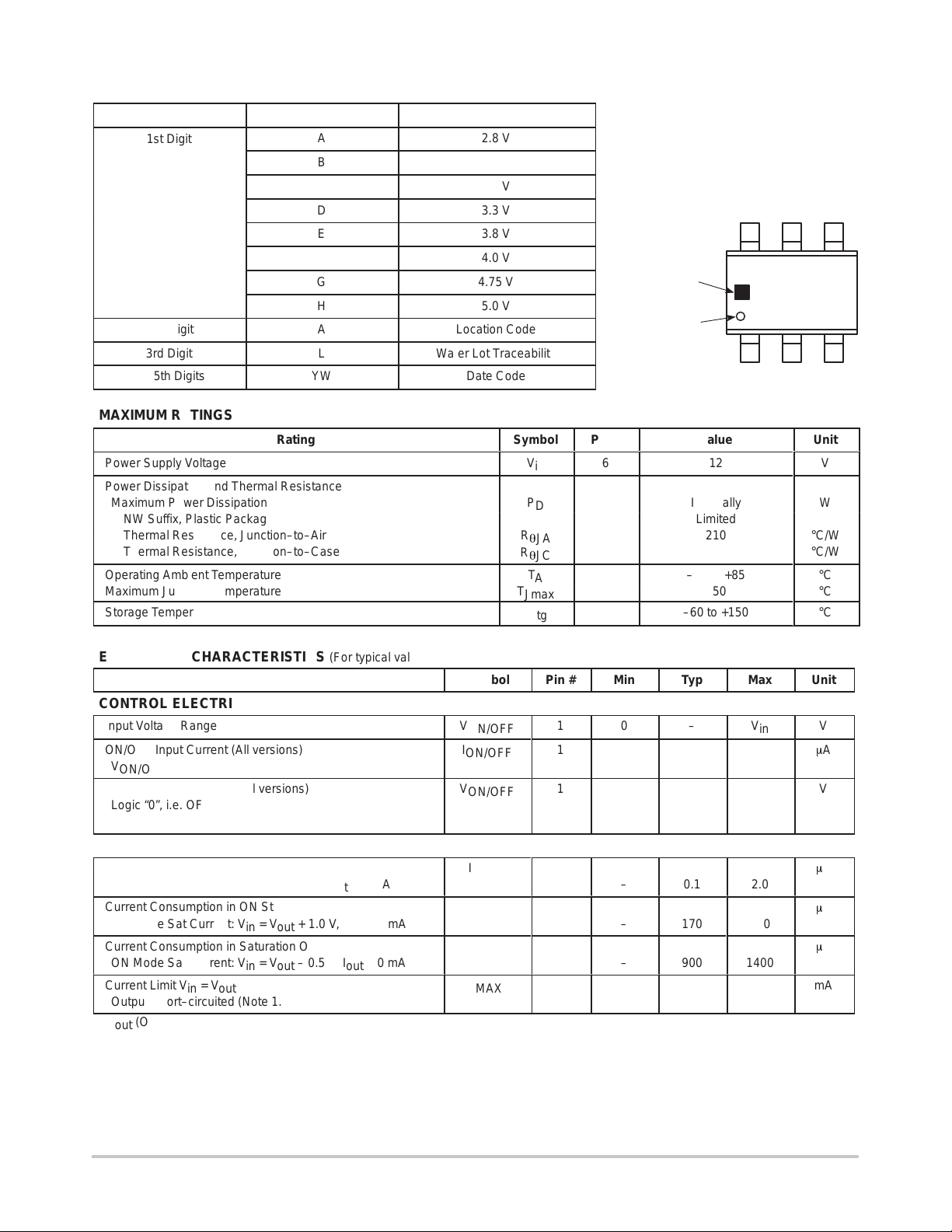
PIN CONNECTIONS
ON/OFF
BYPASS
ORDERING INFORMATION
1
GND
3
(Top View)
xAYLW
1
6
V
IN
52
GND
4
V
OUT
2500 Tape & Reel
2500 Tape & Reel
* Current Limit
* Antisaturation
* Protection
2
GND
Semiconductor Components Industries, LLC, 2000
April, 2000 – Rev. 2
5
GND
1 Publication Order Number:
MC33263/D
Page 2
MC33263
ÁÁÁ
ÁÁÁ
ÁÁÁ
ÁÁÁ
ÁÁÁ
DEVICE MARKING
XALYW Marking Version
1st Digit
A
B
C
D
E
F
G
H
2nd Digit
3rd Digit
A
L
4th/5th Digits YW Date Code
MAXIMUM RATINGS
Rating Symbol Pin # Value Unit
Power Supply Voltage
Power Dissipation and Thermal Resistance
Maximum Power Dissipation P
NW Suffix, Plastic Package Limited
Thermal Resistance, Junction–to–Air
Thermal Resistance, Junction–to–Case
Operating Ambient Temperature
Maximum Junction Temperature
Storage Temperature Range
2.8 V
3.0 V
3.2 V
3.3 V
3.8 V
4.0 V
4.75 V
5.0 V
Location Code
Wafer Lot Traceability
V
in
D
R
q
JA
R
q
JC
T
A
T
Jmax
T
stg
Pin 1 Ink
Mark Identifier
Solid Pin 1 Dot
or Dimple
6
65 4
or
XALYW
12 3
SOT–23L
12
Internally W
210 °C/W
–40 to +85
150
–60 to +150
V
°C/W
°C
°C
°C
ELECTRICAL CHARACTERISTICS (For typical values T
Characteristics
= 25°C, for min/max values TA = –40°C to +85°C, Max TJ = 150°C)
A
Symbol Pin # Min Typ Max Unit
CONTROL ELECTRICAL CHARACTERISTICS
Input Voltage Range V
ON/OFF Input Current (All versions)
V
ON/OFF
= 2.4 V – 2.5 –
ON/OFF Input Voltages (All versions)
ON/OFF
I
ON/OFF
V
ON/OFF
Logic “0”, i.e. OFF State – – 0.3
Logic “1”, i.e. ON State 2.2 – –
1 0 – V
1
1
CURRENTS PARAMETERS
Current Consumption in OFF State (All versions)
OFF Mode Current: Vin = V
+ 1.0 V, I
out
= 0 mA – 0.1 2.0
out
Current Consumption in ON State (All versions)
ON Mode Sat Current: Vin = V
+ 1.0 V, I
out
= 0 mA – 170 200
out
Current Consumption in Saturation ON State (All versions)
ON Mode Sat Current: Vin = V
Current Limit Vin = V
+ 1.0 V, (All versions)
out
– 0.5 V, I
out
= 0 mA – 900 1400
out
Output Short–circuited (Note 1.) 175 210 –
1. I
(Output Current) is the measured current when the output voltage drops below 0.3 V with respect to V
out
IQ
IQ
IQ
I
MAX
OFF
ON
SAT
out
at I
= 30 mA.
out
in
V
m
A
V
m
A
m
A
m
A
mA
http://onsemi.com
2
Page 3
MC33263
ELECTRICAL CHARACTERISTICS (For typical values T
Characteristics
Vin = V
2.8 Suffix 2.74 2.8 2.86
3.0 Suffix 2.94 3.0 3.06
3.2 Suffix 3.13 3.2 3.27
3.3 Suffix 3.23 3.3 3.37
3.8 Suffix 3.72 3.8 3.88
4.0 Suffix 3.92 4.0 4.08
4.75 Suffix 4.66 4.75 4.85
5.0 Suffix 4.90 5.0 5.1
Vin = V
1.0 mA < I
2.8 Suffix 2.7 2.8 2.9
3.0 Suffix 2.9 3.0 3.1
3.2 Suffix 3.09 3.2 3.31
3.3 Suffix 3.18 3.3 3.42
3.8 Suffix 3.67 3.8 3.93
4.0 Suffix 3.86 4.0 4.14
4.75 Suffix 4.58 4.75 4.92
5.0 Suffix 4.83 5.0 5.17
+ 1.0 V, TA = 25°C, 1.0 mA < I
out
+ 1.0 V, –40°C < TA < 80°C, V
out
< 150 mA
out
< 150 mA
out
= 25°C, for min/max values TA = –40°C to +85°C, Max TJ = 150°C)
A
Symbol Pin # Min Typ Max Unit
V
out
out
4
4 V
LINE AND LOAD REGULATION, DROPOUT VOLTAGES
Line Regulation (All versions)
V
+ 1.0 V < Vin < 12 V, I
out
Load Regulation (All versions) Vin = V
Dropout Voltage (All versions)
= 60 mA – 2.0 10
out
I
= 1.0 to 60 mA
out
I
= 1.0 to 100 mA
out
I
= 1.0 to 150 mA
out
I
= 10 mA – 30 90
out
I
= 100 mA – 137 230
out
I
= 150 mA – 180 260
out
out
+ 1.0 V
Reg
Reg
Vin – V
line
load
out
4/6
1
4, 6
–
–
–
8.0
15
20
DYNAMIC PARAMETERS
Ripple Rejection (All versions)
Vin = V
Line Transient Response
Vin = V
d(Vin)/dt = 15 mV/ms
Output Noise Voltage (All versions)
C
out
Output Noise Density
C
out
Output Rise Time (All versions)
C
out
1% of ON/OFF Signal to 99% of Nominal Output Voltage
+ 1.0 V, Vpp = 1.0 V, f = 1.0 kHz, I
out
+ 1.0 V to V
out
= 1.0 µF, I
= 1.0 µF, I
= 1.0 µF, I
out
out
out
+ 4.0 V, I
out
= 60 mA, f = 100 Hz to 100 kHz
= 60 mA, f = 1.0 kHz – 230 –
= 30 mA, V
ON/OFF
= 60 mA 60 70 –
out
= 60 mA, – 1.0 –
out
C
C
C
Without Bypass Capacitor – 40 – µs
With C
= 10 nF – 25 –
bypass
= 1.0 nF – 40 –
bypass
= 0 nF – 65 –
bypass
= 0 to 2.4 V
= 10 nF – 1.1 – ms
bypass
V
RMS
V
N
t
r
4, 6
4, 6
4, 6
4
4
THERMAL SHUTDOWN
Thermal Shutdown (All versions)
–
150
25
35
45
V
mV
mV
mV
dB
mV
µVrms
nV/ √Hz
–
°C
http://onsemi.com
3
Page 4

MC33263
DEFINITIONS
Load Regulation – The change in output voltage for a
change in load current at constant chip temperature.
Dropout V oltage – The input/output differential at which
the regulator output no longer maintains regulation against
further reductions in input voltage. Measured when the
output drops 100 mV below its nominal value (which is
measured at 1.0 V differential), dropout voltage is affected
by junction temperature, load current and minimum input
supply requirements.
Output Noise Voltage – The RMS AC voltage at the
output with a constant load and no input ripple, measured
over a specified frequency range.
Maximum Power Dissipation – The maximum total
dissipation for which the regulator will operate within
specifications.
Quiescent Current – Current which is used to operate the
regulator chip and is not delivered to the load.
Line Regulation – The change in input voltage for a
change in the input voltage. The measurement is made under
conditions of low dissipation or by using pulse techniques
such that the average chip temperature is not significantly
affected.
Line Transient Response – Typical over– and
undershoot response when input voltage is excited with a
given slope.
Thermal Protection – Internal thermal shutdown
circuitry is provided to protect the integrated circuit in the
event that the maximum junction temperature is exceeded.
When activated, typically 150°C, the regulator turns off.
This feature is provided to prevent catastrophic failures from
accidental overheating.
Maximum Package Power Dissipation – The maximum
package power dissipation is the power dissipation level at
which the junction temperature reaches its maximum value
i.e. 125°C. The junction temperature is rising while the
difference between the input power (VCC X ICC) and the
output power (V
out
X I
out
) is increasing.
Depending on ambient temperature, it is possible to
calculate the maximum power dissipation, maximum load
current or maximum input voltage (see Application Hints:
Protection).
The maximum power dissipation supported by the device
is a lot increased when using appropriate application design.
Mounting pad configuration on the PCB, the board material
and also the ambient temperature are affected the rate of
temperature rise. It means that when the IC has good thermal
conductivity through PCB, the junction temperature will be
“low” even if the power dissipation is great.
The thermal resistance of the whole circuit can be
evaluated by deliberately activating the thermal shutdown
of the circuit (by increasing the output current or raising the
input voltage for example).
Then you can calculate the power dissipation by
subtracting the output power from the input power. All
variables are then well known: power dissipation, thermal
shutdown temperature (150°C for MC33263) and ambient
temperature.
APPLICATION HINTS
Input Decoupling – As with any regulator, it is necessary
to reduce the dynamic impedance of the supply rail that
feeds the component. A 1 mF capacitor either ceramic or
tantalum is recommended and should be connected close to
the MC33263 package. Higher values will correspondingly
improve the overall line transient response.
Output Decoupling – Thanks to a novel concept, the
MC33263 is a stable component and does not require any
Equivalent Series Resistance (ESR) neither a minimum
output current. Capacitors exhibiting ESRs ranging from a
few mW up to 3W can thus safely be used. The minimum
decoupling value is 1 mF and can be augmented to fulfill
stringent load transient requirements. The regulator accepts
ceramic chip capacitors as well as tantalum devices.
Noise Performances – Unlike other LDOs, the MC33263
is a true low–noise regulator. W ith a 10 nF bypass capacitor ,
it typically reaches the incredible level of 25 mVRMS overall
noise between 100 Hz and 100 kHz. To give maximum
insight on noise specifications, ON Semiconductor includes
spectral density graphics as well as noise dependency versus
bypass capacitor .
The bypass capacitor impacts the start–up phase of the
MC33263 as depicted by the data–sheet curves. A typical
1 ms settling time is achieved with a 10 nF bypass capacitor.
However, thanks to its low–noise architecture, the
MC33263 can operate without bypass and thus offers a
typical 20 ms start–up phase. In that case, the typical output
noise stays lower than 65 mVRMS between 100 Hz –
100 kHz.
Protections – The MC33263 hosts several protections,
conferring natural ruggedness and reliability to the products
implementing the component. The output current is
internally limited to a minimum of 175 mA while
temperature shutdown occurs if the die heats up beyond
150°C. These value lets you assess the maximum
differential voltage the device can sustain at a given output
current before its protections come into play.
The maximum dissipation the package can handle is given
by:
T
P
max
Jmax–TA
+
R
q
JA
http://onsemi.com
4
Page 5

MC33263
Inp
Outp
Diff
–
)
If T
is internally limited to 150°C, then the MC33263
Jmax
can dissipate up to 595 mW @ 25°C.
The power dissipated by the MC33263 can be calculated
from the following formula:
Ptot
+ǀVin@
I
gnd
(I
)
ǁ ) ǀ
Vin*
V
ǁ @
out
out
I
out
or
Vin
max
Ptot)V
+
I
gnd
out
)
I
@
out
I
out
If a 150 mA output current is needed, the ground current
is extracted from the data–sheet curves: 6.5 mA @ 150 mA.
For a MC33263NW28R2 (2.8 V), the maximum input
voltage will then be 6.48 V, a rather comfortable margin.
T ypical Application – The following figure portraits the
typical application for the MC33263 where both
input/output decoupling capacitors appear.
ut
654
ut
Figure 2. Printed Circuit Board
erential (V
V
in
out
C3
1.0 mF
On/Off
Figure 1. A T ypical MC33263 Application with
Recommended Capacitor Values
MC33263
123
C1
10 nF
C2
1.0 mF
As for any low noise designs, particular care has to be
taken when tackling Printed Circuit Board (PCB) layout.
The following figure gives an example of a layout where
stray inductances/capacitances are minimized.
MC33263
Input Output
Figure 3. Copper Side Component Layout
C3
++
Rpull–up
ON/OFF
C2
C1
This layout is the basis for an MC33263 performance
evaluation board where the BNC connectors give the user an
easy and quick evaluation mean.
http://onsemi.com
5
Page 6

MC33263
MC33263 Wake–up Improvement – In portable
applications, an immediate response to an enable signal is
vital. If noise is not of concern, the MC33263 without a
bypass capacitor settles in nearly 20 ms and typically delivers
65 mVRMS between 100 Hz and 100 kHz.
In ultra low–noise systems, the designer needs a 10 nF
bypass capacitor to decrease the noise down to 25 mVRMS
between 100 Hz and 100 kHz. With the adjunction of the
10 nF capacitor, the wake–up time expands up to 1 ms as
shown on the data–sheet curves. If an immediate response
is wanted, following figure’s circuit gives a solution to
charge the bypass capacitor with the enable signal without
degrading the noise response of the MC33263.
At power–on, C4 is discharged. When the control logic
sends its wake–up signal by going to a high level, the PNP
base is momentarily tight to ground. The PNP switch closes
and immediately charges the bypass capacitor C1 toward its
operating value. After a few ms, the PNP opens and becomes
totally transparent to the regulator.
This circuit improves the response time of the regulator
which drops from 1 ms down to 30 ms. The value of C4 needs
to be tweaked in order to avoid any bypass capacitor
overload during the wake–up transient.
Input Output
654
++
C3
1.0 mF
On/Off
R2
220 k
C4
470 pF
MC33263
123
MMBT2902LT1
Q1
C1
10 nF
C2
1.0 mF
Figure 4. A PNP Transistor Drives the
Bypass Pin when Enable Goes High
MC33263 Without
Wake–up Improvement
(Typical Response)
1 ms
MC33263 With
Wake–up Improvement
(Typical Response)
30 ms
Figure 5. MC33263 Wake–up Improvement with Small PNP Transistor
http://onsemi.com
6
Page 7

MC33263
The PNP being wired upon the bypass pin, it shall not
degrade the noise response of the MC33263. Figure 6
confirms the good behavior of the integrated circuit in this
350
300
250
200
C
= 10 nF
150
nV/sqrt (Hz)
100
50
byp
Vin = 26 mVrms C = 10 nF
@ 100 Hz – 100 kHz
0
100 1,000
Figure 6. Noise Density of the MC33263 with a
10 nF Bypass Capacitor and a Wake–up
Improvement Network
area which reaches a typical noise level of 26 mVRMS
(100 Hz to 100 kHz) at I
10,000
Frequency (Hz)
Vin = 3.8 V
V
= 2.8 V
out
Co = 1.0 mF
I
= 60 mA
out
T
amb
100,000
= 25°C
out
1,000,000
= 60 mA.
http://onsemi.com
7
Page 8

MC33263
TYPICAL PERFORMANCE CHARACTERISTICS
Ground Current Performances
7.0
Vin = 3.8 V
6.0
V
= 2.8 V
out
CO = 1.0 mF
5.0
T
= 25°C
amb
4.0
3.0
2.0
GROUND CURRENT (mA)
1.0
0
0
20 40 100 –20 0 20 40 60 80
60 80 120 140 200160 180
OUTPUT CURRENT (mA)
Figure 7. Ground Current versus Output Current
Line Transient Response and Output Voltage
200
m
190
180
170
160
150
140
130
120
110
QUIESCENT CURRENT ON MODE ( A)
100
–40
–20
0204060 10080
TEMPERATURE (°C)
GROUND CURRENT (mA)
2.1
2.05
2.0
1.95
1.9
1.85
1.8
–40
AMBIENT TEMPERATURE (°C)
Figure 8. Ground Current versus Ambient
Temperature
Vin = 3.8 to 7.0 V
Y1 = 1.0 mV/div
Y2 = 1.0 V/div
X = 1.0 ms
I
= 60 mA
out
T
= 25°C
amb
dVin = 3.2 V
Vin = 3.8 V
V
= 2.8 V
out
CO = 1.0 mF
I
= 60 mA
out
Y1
Y2
Figure 9. Quiescent Current versus T emperature Figure 10. Line Transient Response
http://onsemi.com
8
Page 9

Vin = 3.8 V
Y1 = 100 mV/div
Y2 = 20 mV/div
X = 200 ms/div
T
= 25°C
amb
MC33263
TYPICAL PERFORMANCE CHARACTERISTICS
Load Transient Response versus Load Current Slope
Y2
Vin = 3.8 V
Y1 = 50 mA/div
Y2 = 20 mV/div
X = 20 ms
T
= 25°C
Y1
amb
Y1: OUTPUT CURRENT, Y2: OUTPUT VOLTAGEY1: OUTPUT CURRENT, Y2: OUTPUT VOLTAGE
Y1
Y2
Figure 11. I
Vin = 3.8 V
Y1 = 50 mA/div
Y2 = 20 mV/div
X = 100 ms
T
= 25°C
amb
Figure 13. I
= 3.0 mA to 150 mA
out
= 6.0 mA/ms (Large Scale)
Slope
I
= 3.0 mA to 150 mA
out
Y1
Y2
Figure 12. I
Vin = 3.8 V
Y1 = 50 mA/div
Y2 = 20 mV/div
X = 200 ms
T
= 25°C
amb
Y1: OUTPUT CURRENT, Y2: OUTPUT VOLTAGEY1: OUTPUT CURRENT, Y2: OUTPUT VOLTAGE
Figure 14. I
= 100 mA/ms (Large Scale)
Slope
I
= 3.0 mA to 150 mA
out
= 2.0 mA/ms (Large Scale)
Slope
I
= 3.0 mA to 150 mA
out
Y1
Y2
http://onsemi.com
9
Page 10

MC33263
TYPICAL PERFORMANCE CHARACTERISTICS
Noise Performances
350
300
250
200
nV/Hz
150
100
Vn = 65 mVrms @ C
Vn = 30 mVrms @ C
50
Vn = 25 mVrms @ C
over 100 Hz to 100 kHz
0
100
1200
1000
m
800
600
400
SETTLING TIME ( S)
200
0
0
100,000
Vin = 3.8 V
V
= 2.8 V
out
CO = 1.0 mF
I
= 60 mA
out
T
= 23°C
amb
1,000,000
C
= 10 nF
byp
1000 10,000
3.3 nF
= 0
bypass
= 3.3 nF
bypass
= 10 nF
bypass
FREQUENCY (Hz)
0 nF
Figure 15. Noise Density versus Bypass
Capacitor
Settling Time Performances
Vin = 3.8 V
V
= 2.8 V
out
CO = 1.0 mF
I
= 60 mA
out
T
= 25°C
amb
1.0 2.0 3.0 4.0 6.0 10
BYPASS CAPACITOR (nF)
5.0 7.0 9.08.0
70
60
50
m
40
30
20
10
0
Vin = 3.8 V
V
out
CO = 1.0 mF
I
out
T
amb
0
1.0
= 2.8 V
= 60 mA
= 25°C
2.0 3.0 4.0 5.0
BYPASS CAPACITOR (nF)
6.0 7.0 8.0 9.0
RMS NOISE ( V)
Figure 16. RMS Noise versus Bypass Capacitor
(100 Hz – 100 kHz)
200 ms/div
500 mV/div
C
= 10 nF
byp
Vin = 3.8 V
V
= 2.8 V
out
C
= 1.0 mF
out
I
= 50 mA
out
T
= 25°C
amb
10
Figure 17. Output Voltage Settling Time versus
Bypass Capacitor
Vin = 3.8 V
V
= 2.8 V
out
C
100 ms/div
500 mV/div
C
= 3.3 nF
byp
I
T
out
out
amb
= 1.0 mF
= 50 mA
= 25°C
Figure 19. Output Voltage Settling Shape
C
bypass
= 3.3 nF
http://onsemi.com
10
Figure 18. Output V oltage Settling Shape
C
bypass
= 10 nF
10 ms/div
500 mV/div
C
= 0 nF
byp
Vin = 3.8 V
V
= 2.8 V
out
C
= 1.0 mF
out
I
= 50 mA
out
T
= 25°C
amb
Figure 20. Output Voltage Settling Shape without
Bypass Capacitor
Page 11

MC33263
TYPICAL PERFORMANCE CHARACTERISTICS
Dropout Voltage
250
200
150
100
DROPOUT (mV)
50
0
10 60
Figure 21. Dropout V oltage versus I
IO (mA)
100
85°C
25°C
–40°C
150
out
250
200
150
100
DROPOUT (mV)
50
0
–40
–20 0 20
TEMPERATURE (°C)
Figure 22. Dropout V oltage versus Temperature
Output Voltage
2.805
2.800
2.795
2.790
2.785
2.780
OUTPUT VOLTAGE (V)
2.775
2.770
–20 0 40 100
–40
20 8060
TEMPERATURE (°C)
1 mA
60 mA
100 mA
150 mA
2.860
2.840
2.820
2.800
2.780
OUTPUT VOLTAGE (V)
2.760
2.740
0
20 40 80 160
60 120100
OUTPUT CURRENT (mA)
Figure 23. Output V oltage versus Temperature Figure 24. Output V oltage versus I
10 mA
60 mA
100 mA
150 mA
40 60 80
25°C
85°C
out
100
–40°C
140
Ripple Rejection Performances
0
–10
Vin = 3.8 V
V
= 2.8 V
CO = 1.0 mF
I
T
100
out
= 60 mA
out
amb
= 25°C
1000 100,000
FREQUENCY (Hz)
10,000
(dB)
–20
–30
–40
–50
–60
–70
–80
–90
–100
Figure 25. Ripple Rejection versus Frequency with
10 nF Bypass Capacitor
0
–20
–40
–60
(dB)
–80
–100
–120
10
http://onsemi.com
11
Vin = 3.8 V
V
= 2.8 V
out
CO = 1.0 mF
I
= 60 mA
out
T
= 25°C
amb
100
1000 100,000
FREQUENCY (Hz)
10,000
1,000,000
Figure 26. Ripple Rejection versus Frequency
without Bypass Capacitor
Page 12

PIN 1 IDENTIFIER
IN THIS ZONE
D
A
MC33263
P ACKAGE DIMENSIONS
SOT–23L
NW SUFFIX
CASE 318J–01
ISSUE B
NOTES:
1. DIMENSIONS ARE IN MILLIMETERS.
0.05
E
M
0.20 C
M
B
C
S
B
E1
A
6
e
5
A
4
e1
B
1
2
3
A1
A
S
A
M
b
0.10 C
(b)
q
c1
H
L
c
b1
SECTION A–A
2. INTERPRET DIMENSIONS AND TOLERANCES
PER ASME Y14.5M, 1994.
3. DIMENSION E1 DOES NOT INCLUDE INTERLEAD
FLASH OR PROTRUSION. INTERLEAD FLASH OR
PROTRUSION SHALL NOT EXCEED 0.23 PER
SIDE.
4. DIMENSIONS b AND b2 DO NOT INCLUDE
DAMBAR PROTRUSION. ALLOWABLE DAMBAR
PROTRUSION SHALL BE 0.08 TOTAL IN EXCESS
OF THE b AND b2 DIMENSIONS AT MAXIMUM
MATERIAL CONDITION.
5. TERMINAL NUMBERS ARE SHOWN FOR
REFERENCE ONLY.
6. DIMENSIONS D AND E1 ARE TO BE DETERMINED
AT DATUM PLANE H.
MILLIMETERS
DIM MIN MAX
A 1.25 1.40
A1 0.00 0.10
b 0.35 0.50
b1 0.35 0.45
c 0.10
c1 0.10
D 3.20
E 3.00 3.60
E1 2.00 2.40
e
e1
L 0.25
q
0.25
0.20
3.60
0.95
1.90
0.55
0 10
__
ON Semiconductor and are trademarks of Semiconductor Components Industries, LLC (SCILLC). SCILLC reserves the right to make changes
without further notice to any products herein. SCILLC makes no warranty , representation or guarantee regarding the suitability of its products for any particular
purpose, nor does SCILLC assume any liability arising out of the application or use of any product or circuit, and specifically disclaims any and all liability ,
including without limitation special, consequential or incidental damages. “Typical” parameters which may be provided in SCILLC data sheets and/or
specifications can and do vary in different applications and actual performance may vary over time. All operating parameters, including “Typicals” must be
validated for each customer application by customer’s technical experts. SCILLC does not convey any license under its patent rights nor the rights of others.
SCILLC products are not designed, intended, or authorized for use as components in systems intended for surgical implant into the body, or other applications
intended to support or sustain life, or for any other application in which the failure of the SCILLC product could create a situation where personal injury or
death may occur. Should Buyer purchase or use SCILLC products for any such unintended or unauthorized application, Buyer shall indemnify and hold
SCILLC and its officers, employees, subsidiaries, affiliates, and distributors harmless against all claims, costs, damages, and expenses, and reasonable
attorney fees arising out of, directly or indirectly , any claim of personal injury or death associated with such unintended or unauthorized use, even if such claim
alleges that SCILLC was negligent regarding the design or manufacture of the part. SCILLC is an Equal Opportunity/Affirmative Action Employer .
PUBLICATION ORDERING INFORMATION
NORTH AMERICA Literature Fulfillment:
Literature Distribution Center for ON Semiconductor
P.O. Box 5163, Denver, Colorado 80217 USA
Phone: 303–675–2175 or 800–344–3860 Toll Free USA/Canada
Fax: 303–675–2176 or 800–344–3867 Toll Free USA/Canada
Email: ONlit@hibbertco.com
Fax Response Line: 303–675–2167 or 800–344–3810 T oll Free USA/Canada
N. American Technical Support: 800–282–9855 Toll Free USA/Canada
EUROPE: LDC for ON Semiconductor – European Support
German Phone: (+1) 303–308–7140 (M–F 1:00pm to 5:00pm Munich Time)
Email: ONlit–german@hibbertco.com
French Phone: (+1) 303–308–7141 (M–F 1:00pm to 5:00pm Toulouse T ime)
Email: ONlit–french@hibbertco.com
English Phone: (+1) 303–308–7142 (M–F 12:00pm to 5:00pm UK Time)
Email: ONlit@hibbertco.com
EUROPEAN TOLL–FREE ACCESS*: 00–800–4422–3781
*Available from Germany, France, Italy, England, Ireland
CENTRAL/SOUTH AMERICA:
Spanish Phone: 303–308–7143 (Mon–Fri 8:00am to 5:00pm MST)
Email: ONlit–spanish@hibbertco.com
ASIA/PACIFIC : LDC for ON Semiconductor – Asia Support
Phone: 303–675–2121 (Tue–Fri 9:00am to 1:00pm, Hong Kong Time)
T oll Free from Hong Kong & Singapore:
001–800–4422–3781
Email: ONlit–asia@hibbertco.com
JAPAN: ON Semiconductor, Japan Customer Focus Center
4–32–1 Nishi–Gotanda, Shinagawa–ku, T okyo, Japan 141–8549
Phone: 81–3–5740–2745
Email: r14525@onsemi.com
ON Semiconductor Website: http://onsemi.com
For additional information, please contact your local
Sales Representative.
http://onsemi.com
12
MC33263/D
 Loading...