

Page 1
MC33260
Product Preview
GreenLine
Compact
Power Factor Controller:
Innovative Circuit for
Cost Effective Solutions
The MC33260 is a controller for Power Factor Correction
preconverters meeting international standard requirements in
electronic ballast and off–line power conversion applications.
Designed to drive a free frequency discontinuous mode, it can also be
synchronized and in any case, it features very effective protections that
ensure a safe and reliable operation.
This circuit is also optimized to offer extremely compact and cost
effective PFC solutions. While it requires a minimum number of
external components, the MC33260 can control the follower boost
operation that is an innovative mode allowing a drastic size reduction
of both the inductor and the power switch. Ultimately, the solution
system cost is significantly lowered.
Also able to function in a traditional way (constant output voltage
regulation level), any intermediary solutions can be easily
implemented. This flexibility makes it ideal to optimally cope with a
wide range of applications.
General Features
• Standard Constant Output Voltage or “Follower Boost” Mode
• Switch Mode Operation: Voltage Mode
• Latching PWM for Cycle–by–Cycle On–Time Control
• Constant On–Time Operation That Saves the Use of an Extra Multiplier
• Totem Pole Output Gate Drive
• Undervoltage Lockout with Hysteresis
• Low Start–Up and Operating Current
• Improved Regulation Block Dynamic Behavior
• Synchronization Capability
• Internally Trimmed Reference Current Source
Safety Features
• Overvoltage Protection: Output Overvoltage Detection
• Undervoltage Protection: Protection Against Open Loop
• Effective Zero Current Detection
• Accurate and Adjustable Maximum On–Time Limitation
• Overcurrent Protection
• ESD Protection on Each Pin
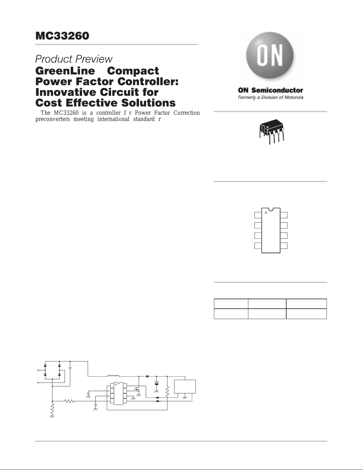
http://onsemi.com
8
1
DIP–8
P SUFFIX
CASE 626
PIN CONNECTIONS AND
MARKING DIAGRAM
AWL
YYWW
V
CC
Gate Drive
7
Gnd
6
Synchronization
5
Input
Feedback Input
V
control
Oscillator
Capacitor (CT)
Current Sense
Input
AWL = Manufacturing Code
18
2
3
MC33260
4
YYWW = Date Code
(Top View)
ORDERING INFORMATION
Device Package Shipping
MC33260P Plastic DIP–8 50 Units / Rail
TYPICAL APPLICATION
D1...D4
R
cs
This document contains information on a product under development. ON Semiconductor
reserves the right to change or discontinue this product without notice.
Semiconductor Components Industries, LLC, 1999
November, 1999 – Rev. 1
Filtering
Capacitor
V
control
R
OCP
L1
8
1
2
7
3
6
MC33260
4
CT
5
V
Sync
D1
C1
CC
+
M1
LOAD
(SMPS, Lamp
Ballast,...)
R
o
1 Publication Order Number:
MC33260/D
Page 2
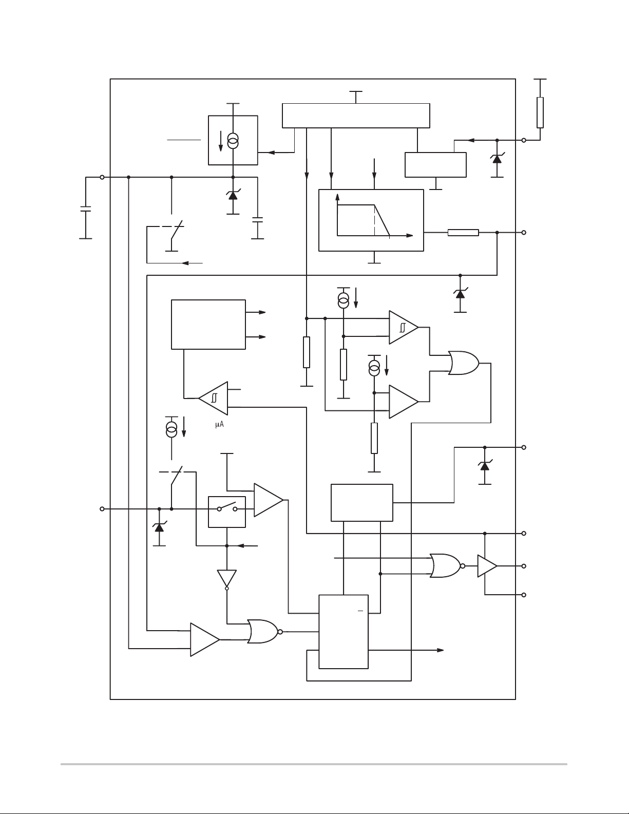
CT
MC33260
BLOCK DIAGRAM
V
o
Current Mirror
2 x IO x I
I
– ch =
OSC
3
O
I
ref
11 V
I
o
I
oIo
I
ref
V
ref
1.5 V
Current
Mirror
I
o
FB
1
Current
Sense
01
Output_Ctrl
REGULATOR
Enable
–
+
Ics (205 mA)
–60 mV
01
4
11 V
LEB
15 pF
V
ref
I
ref
11 V/8.5 V
+
–
Output_Ctrl
300 k
V
reg
I
o
97%I
r
r
Synchro
Arrangement
I
ref
ref
I
ovpH/IovpL
r
I
+
–
uvp
+
–
11 V
OVP
UVP
11 V
V
control
2
Synchro
5
V
CC
8
+
–
PWM Comparator
ThStdwn
S
R
PWM
R
Latch
RQ
http://onsemi.com
2
Drive
7
Gnd
6
Q
Output_Ctrl
MC33260
Page 3
MC33260
MAXIMUM RATINGS
Rating Pin # Symbol Value Unit
Gate Drive Current (Pin 7)*
Source
Sink
VCC (Pin 8) Maximum Voltage 8 (Vcc)
Input Voltage V
Power Dissipation and Thermal Characteristics
P Suffix, DIP Package
Maximum Power Dissipation @ TA = 85°C
Thermal Resistance Junction to Air
Operating Junction Temperature T
Operating Ambient Temperature T
*The maximum package power dissipation must be observed.
7
I
O(Source)
I
O(Sink)
max
in
P
D
R
θJA
J
A
–500
500
16 V
–0.3 to +10 V
600
100
150 °C
–40 to +105 °C
mA
mW
°C/W
ELECTRICAL CHARACTERISTICS (V
unless otherwise noted.)
Characteristic
GATE DRIVE SECTION
Gate Drive Resistor
Source Resistor @ I
Sink Resistor @ I
Gate Drive Voltage Rise Time (From 3 V Up to 9 V)
(Note 1)
Output Voltage Falling Time (From 9 V Down to 3 V)
(Note 1)
OSCILLATOR SECTION
Maximum Oscillator Swing 3 ∆V
Charge Current @ I
Charge Current @ I
Ratio Multiplier Gain Over Maximum Swing
@ I
=100 µA
pin1
Ratio Multiplier Gain Over Maximum Swing
@ I
=200 µA
pin1
Average Internal Pin 3 Capacitance Over Oscillator
Maximum Swing (V
(Note 2)
Discharge Time (CT = 1 nF) 3 T
REGULATION SECTION
Regulation High Current Reference 1 I
Ratio (Regulation Low Current Reference)/I
Pin 2 Impedance 1 Z
Pin 1 Clamp Voltage @ I
Pin 1 Clamp Voltage @ I
pin1
pin1
= 100 mA
pin7
= 100 mA
pin7
= 100 µA 3 I
= 200 µA 3 I
Varying From 0 Up to 1.5 V)
pin3
= 100 µA 1 V
pin1
= 200 µA 1 V
pin1
= 13 V, TJ = 25°C for typical values, TJ = –40 to 105°C for min/max values
CC
Pin # Symbol Min Typ Max Unit
7
7 t
7 t
3 K
3 K
3 C
reg–H
1 I
reg–L/Ireg–H
R
OL
R
OH
r
f
T
charge
charge
osc
osc
int
disch
reg–H
pin3
pin1–100
pin1–200
10
5
— 50 — ns
— 50 — ns
1.4 1.5 1.6 V
87.5 100 112.5 µA
350 400 450 µA
5600 6400 7200 1/(V.A)
5600 6400 7200 1/(V.A)
10 15 20 pF
— 0.5 1 µs
192 200 208 µA
0.965 0.97 0.98 —
— 300 — kΩ
1.5 2.1 2.5 V
2 2.6 3 V
20
10
35
25
Ω
http://onsemi.com
3
Page 4
MC33260
ELECTRICAL CHARACTERISTICS (V
unless otherwise noted.)
Characteristic UnitMaxTypMinSymbolPin #
CURRENT SENSE SECTION
Zero Current Detection Comparator Threshold 4 V
Negative Clamp Level (I
Bias Current @ V
Propagation Delay (V
Pin 4 Internal Current Source 4 I
Leading Edge Blanking Duration τ
OverCurrent Protection Propagation Delay
(Pin 4 < V
SYNCHRONIZATION SECTION
Synchronization Threshold 5 V
Negative Clamp Level (I
Minimum Off–Time 7 T
Minimum Required Synchronization Pulse Duration 5 T
OVERVOLTAGE PROTECTION SECTION
OverVoltage Protection High Current Threshold
and I
reg–H
OverVoltage Protection Low Current Threshold
and I
reg–H
Ratio (I
OVP–H/IOVP–L
Propagation Delay (I
UNDERVOLTAGE PROTECTION SECTION
Ratio (UnderVoltage Protection Current Threshold)/I
Propagation Delay (I
THERMAL SHUTDOWN SECTION
Thermal Shutdown Threshold 7 T
Hysteresis 7 ∆T
VCC UNDERVOLTAGE LOCKOUT SECTION
Start–Up Threshold 8 V
Disable Voltage After Threshold T urn–On 8 V
TOTAL DEVICE
Power Supply Current
Start–Up (VCC = 5 V with VCC Increasing)
Operating @ I
NOTES:
(1) 1 nF being connected between the pin 7 and ground.
(2) Guaranteed by design.
(3) No load is connected to the gate drive which is kept high during the test.
pin4
ZCD–th
Difference
Difference
pin1
= –1 mA) 4 Cl–neg — –0.7 — V
pin2
= V
ZCD–th
> V
pin4
ZCD–th
to Gate Drive Low)
= –1 mA) 5 Cl–neg — –0.7 — V
pin5
) 1 I
pin1
pin1
= 200 µA
> 110% I
< 12% I
to Gate Drive Low) 7 T
ref
to Gate Drive Low) 7 T
ref
= 13 V, TJ = 25°C for typical values, TJ = –40 to 105°C for min/max values
CC
4 I
) to Gate Drive High 7 T
7 T
reg–H
1 I
1 I
1 I
8 I
OVP–H–Ireg–H
OVP–L–Ireg–H
OVP–H/IOVP–L
ZCD–th
b–cs
ZCD
OCP
LEB
OCP
sync–th
off
sync
OVP
UVP/Ireg–H
UVP
stdwn
stdwn
stup–th
disable
CC
–90 –60 –30 mV
–0.2 — — µA
— 500 — ns
192 205 218 µA
— 400 — ns
100 160 240 ns
0.8 1 1.2 V
1.5 2.1 2.7 µs
— — 0.5 µs
8 13 18 µA
0 — — —
1.02 — — —
— 500 — ns
12 14 16 %
— 500 — ns
— 150 — °C
— 30 — °C
9.7 11 12.3 V
7.4 8.5 9.6 V
—
—
0.1
4
0.25
8
mA
http://onsemi.com
4
Page 5
MC33260
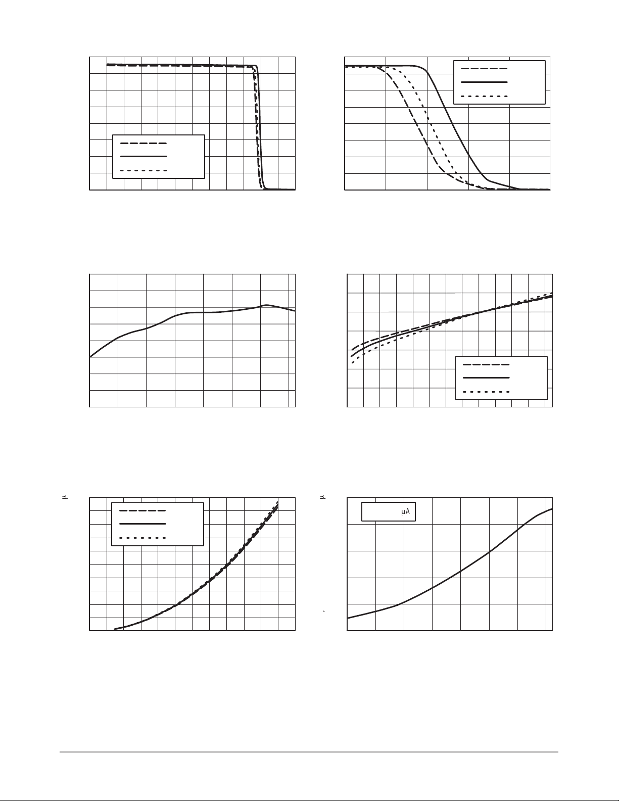
1.6
1.4
1.2
1.0
0.8
control
V : REGULATION BLOCK OUTPUT (V)
0.6
0.4
0.2
0
20
0
60
40
I
pin1
–40°C
25°C
105°C
100
80
: FEEDBACK CURRENT (µA)
120
140
Figure 1. Regulation Block Output versus
Feedback Current
1.340
1.335
1.330
1.325
1.320
1.315
1.310
MAXIMUM OSCILLAT OR SWING (V)I , OSCILLATOR CHARGE CURRENT ( A)
1.305
1.300
–40
–20 0
20
40 60
JUNCTION TEMPERATURE (°C)
160
180
200
80
220
100
240
1.6
1.4
1.2
1.0
0.8
0.6
0.4
0.2
control
V : REGULATION BLOCK OUTPUT (V)
0
185
190 195 200 205 210
I
: FEEDBACK CURRENT (µA)
pin1
Figure 2. Regulation Block Output versus
Feedback Current
3.5
3.0
2.5
2.0
1.5
1.0
FEEDBACK INPUT VOLTAGE (V)
0.5
0
0
20 40 60 80 100 120 140 160 180 200 220 240
I
: FEEDBACK CURRENT (µA)
pin1
–40°C
25°C
105°C
–40°C
25°C
105°C
Figure 3. Maximum Oscillator Swing versus
Temperature
m
500
450
400
350
300
250
200
150
100
50
osc–ch
0
0
20 40 60 80 100 120 140 160 180 200 220 240
I
pin1
–40°C
25°C
105°C
: FEEDBACK CURRENT (µA)
Figure 5. Oscillator Charge Current versus
Feedback Current
Figure 4. Feedback Input Voltage versus
Feedback Current
m
410
I
= 200 mA
pin1
405
400
395
390
385
osc–ch
I , OSCILLATOR CHARGE CURRENT ( A)
–40
–20 0
20
40 60
JUNCTION TEMPERATURE (°C)
Figure 6. Oscillator Charge Current versus
Temperature
80
100
http://onsemi.com
5
Page 6
MC33260
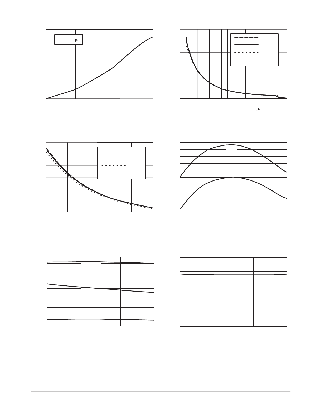
104
103
102
101
100
99
98
OSCILLATOR CHARGE CURRENT ( A)µ
97
I
= 100 mA
pin1
–40
–20 0 20 40 60 80 100
TJ, JUNCTION TEMPERATURE (°C)
Figure 7. Oscillator Charge Current versus
T emperature
75
65
55
45
ON–TIME ( s)µ
35
25
15
50
60 70 80 90 100
I
: FEEDBACK CURRENT (µA)
pin1
1 nF Connected to Pin 3
–40°C
25°C
105°C
120
100
80
60
ON–TIME ( s)µ
40
20
0
30
50 70 90 110 130 150 170 190 210
I
: FEEDBACK CURRENT (mA)
pin1
1 nF Connected to Pin 3
Figure 8. On–Time versus Feedback Current
207
I
206
205
204
203
202
201
200
199
198
197
REGULATION AND CS CURRENT SOURCE ( A)µ
–20 0 20 40 60 80 100
–40
TJ, JUNCTION TEMPERATURE (°C)
OCP
I
regH
–40°C
25°C
105°C
Figure 9. On–Time versus Feedback Current Figure 10. Internal Current Sources versus
T emperature
1.07
)
1.06
ref
/I
1.05
regL
1.04
), (I
1.03
ref
/I
1.02
1.01
ovpL
1.00
), (I
ref
0.99
/I
0.98
ovpH
(I
0.97
0.96
–40
Figure 11. (I
(I
(I
–20 0 20 40 60 80 100
TJ, JUNCTION TEMPERATURE (°C)
ovpH/Iref
ovpH/Iref
ovpL/Iref
(I
regL/Iref
)
)
)
), (I
ovpL/Iref
), (I
regL/Iref
)
versus T emperature
0.150
0.148
ref
/I )
0.146
uvp
0.144
0.142
0.140
0.138
0.136
0.134
UNDERVOLTAGE RATIO (I
0.132
0.130
–20 0 20 40 60 80 100
–40
TJ, JUNCTION TEMPERATURE (°C)
Figure 12. Undervoltage Ratio versus
T emperature
http://onsemi.com
6
Page 7

MC33260
–54.8
–55
–55.2
–55.4
–55.6
–55.8
–56
–56.2
–56.4
–56.6
–20 0 20 40 60 80 100
–40
TJ, JUNCTION TEMPERATURE (°C)
Figure 13. Current Sense Threshold versus
T emperature
20
15
10
–40°C
25°C
4.5
4.0
3.5
3.0
2.5
2.0
1.5
1.0
, CIRCUIT CONSUMPTION (mA)I
CC
0.5
0
2 4 6 8 10 12 14 16
0
–40°C
25°C
105°C
VCC: SUPPLY VOLTAGE (V)
Figure 14. Circuit Consumption versus
Supply V oltage
Vgate
1
25°C
VCC = 12 V
C
I
cross–cond
= 1 nF
gate
(50 mA/div)
105°C
Ch1
10.0 V Ch2210.0 mVWM 1.00ms Ch1 600 mV
OSCILLATOR PIN INTERNAL CAPACITANCE (pF) CURRENT SENSE THRESHOLD (mV)
5
0
0
0.2 0.4 0.6 0.8 1.0 1.2 1.4
V
: PIN 2 VOLTAGE (V)
control
Figure 15. Oscillator Pin Internal Capacitance Figure 16. Gate Drive Cross Conduction
Vgate
–40°C
VCC = 12 V
C
= 1 nF
gate
I
cross–cond
Ch1110.0 V Ch2210.0 mVWM 1.00ms Ch1 600 mV Ch1110.0 V Ch2210.0 mVWM 1.00ms Ch1 600 mV
(50 mA/div)
Vgate
105°C
VCC = 12 V
C
I
cross–cond
gate
= 1 nF
(50 mA/div)
Figure 17. Gate Drive Cross Conduction Figure 18. Gate Drive Cross Conduction
http://onsemi.com
7
Page 8

MC33260
PIN FUNCTION DESCRIPTION
Pin No.
1 Feedback Input This pin is designed to receive a current that is proportional to the preconverter output voltage. This
2 V
3 Oscillator Capacitor
4 Zero Current
5 Synchronization
6 Ground This pin must be connected to the preregulator ground.
7 Gate Drive The gate drive current capability is suited to drive an IGBT or a power MOSFET.
8 V
Function Description
information is used for both the regulation and the overvoltage and undervoltage protections. The
current drawn by this pin is internally squared to be used as oscillator capacitor charge current.
control
(CT)
Detection Input
Input
CC
This pin makes available the regulation block output. The capacitor connected between this pin and
ground, adjusts the control bandwidth. It is typically set below 20 Hz to obtain a nondistorted input
current.
The circuit uses an on–time control mode. This on–time is controlled by comparing the CT voltage to
the V
This pin is designed to receive a negative voltage signal proportional to the current flowing through
the inductor. This information is generally built using a sense resistor. The Zero Current Detection
prevents any restart as long as the pin 4 voltage is below (–60 mV). This pin is also used to perform
the peak current limitation. The overcurrent threshold is programmed by the resistor connected
between the pin and the external current sense resistor.
This pin is designed to receive a synchronization signal. For instance, it enables to synchronize the
PFC preconverter to the associated SMPS. If not used, this pin must be grounded.
This pin is the positive supply of the IC. The circuit turns on when VCC becomes higher than 11 V, the
operating range after start–up being 8.5 V up to 16 V.
voltage. CT is charged by the squared feedback current.
control
R
cs
D1...D4
R
OCP
V
control
CT
APPLICATION SCHEMATIC
Filtering
Capacitor
18
2
3
MC33260
4
L1
D1
C1
+
V
CC
7
6
5
Sync
M1
R
o
Load
(SMPS, Lamp
Ballast,...)
http://onsemi.com
8
Page 9

MC33260
ConverterRectifiers
Load
PFC Preconverter
FUNCTIONAL DESCRIPTION
INTRODUCTION
The need of meeting the requirements of legislation on
line current harmonic content, results in an increasing
demand for cost effective solutions to comply with the
Power Factor regulations. This data sheet describes a
monolithic controller specially designed for this purpose.
Most off–line appliances use a bridge rectifier associated
to a huge bulk capacitor to derive raw dc voltage from the
utility ac line.
ConverterRectifiers
AC
Line
Figure 19. T ypical Circuit Without PFC
+
Bulk
Storage
Capacitor
Load
This technique results in a high harmonic content and in
poor power factor ratios. In effect, the simple rectification
technique draws power from the mains when the
instantaneous ac voltage exceeds the capacitor voltage. This
occurs near the line voltage peak and results in a high charge
current spike. Consequently, a poor power factor (in the
range of 0.5 – 0.7) is generated, resulting in an apparent input
power that is much higher than the real power.
V
pk
Rectified DC
0
Line Sag
AC Line Voltage
AC Line Current
Figure 20. Line Waveforms Without PFC
0
Active solutions are the most popular way to meet the
legislation requirements. They consist of inserting a PFC
pre–regulator between the rectifier bridge and the bulk
capacitor. This interface is, in fact, a step–up SMPS that
outputs a constant voltage while drawing a sinusoidal
current from the line.
OPERATION DESCRIPTION
The MC33260 is optimized to just as well drive a free
running as a synchronized discontinuous voltage mode.
It also features valuable protections (overvoltage and
undervoltage protection, overcurrent limitation, ...) that
make the PFC preregulator very safe and reliable while
requiring very few external components. In particular, it is
able to safely face any uncontrolled direct charges of the
output capacitor from the mains which occur when the
output voltage is lower than the input voltage (start–up,
overload, ...).
In addition to the low count of elements, the circuit can
control an innovative mode named “Follower Boost” that
permits to significantly reduce the size of the preconverter
inductor and power MOSFET. With this technique, the
output regulation level is not forced to a constant value, but
can vary according to the a.c. line amplitude and to the
power. The gap between the output voltage and the ac line
is then lowered, what allows the preconverter inductor and
power MOSFET size reduction. Finally, this method brings
a significant cost reduction.
A description of the functional blocks is given below.
REGULATION SECTION
Connecting a resistor between the output voltage to be
regulated and the pin 1, a feedback current is obtained.
Typically, this current is built by connecting a resistor
between the output voltage and the pin 1. Its value is then
given by the following equation:
Vo*
V
I
pin1
+
pin1
R
o
where:
Ro is the feedback resistor,
Vo is the output voltage,
V
is the pin 1 clamp value.
pin1
The feedback current is compared to the reference current
so that the regulation block outputs a signal following the
characteristic depicted in Figure 22. According to the power
and the input voltage, the output voltage regulation level
varies between two values (Vo)
corresponding to the I
Regulation Block Output
1.5 V
regL
and I
regH
and (Vo)
regL
levels.
regH
AC
Line
High Frequency
Bypass Capacitor
Figure 21. PFC Preconverter
The MC33260 was developed to control an active solution
MC33260
+
Capacitor
Bulk Storage
with the goal of increasing its robustness while lowering its
global cost.
http://onsemi.com
I
reg–L
(97%I
)
ref
Figure 22. Regulation Characteristic
I
reg–H
(I
ref
)
The feedback resistor must be chosen so that the feedback
current should equal the internal current source I
9
regH
I
o
when
Page 10

MC33260
the output voltage exceeds the chosen upper regulation
voltage [(Vo)
In practice, V
equation can be simplified as follows (I
]. Consequently:
regH
ǒ
Ǔ
V
o
Ro+
is small compared to (Vo)
pin1
regH
I
*
regH
V
pin1
regH
regH
and this
being also
replaced by its typical value 200 µA):
Ǔ
<
Ro[5 ǒV
o
regH
>
k
W
The regulation block output is connected to the pin 2
through a 300 kΩ resistor. The pin 2 voltage (V
control
) is
compared to the oscillator sawtooth for PWM control.
An external capacitor must be connected between pin 2
and ground, for external loop compensation. The bandwidth
is typically set below 20 Hz so that the regulation block
output should be relatively constant over a given ac line
cycle. This integration that results in a constant on–time over
the ac line period, prevents the mains frequency output
ripple from distorting the ac line current.
OSCILLATOR SECTION
The oscillator consists of three phases:
• Charge Phase: The oscillator capacitor voltage grows
up linearly from its bottom value (ground) until it
exceeds V
(regulation block output voltage). At
control
that moment, the PWM latch output gets low and the
oscillator discharge sequence is set.
• Discharge Phase: The oscillator capacitor is abruptly
discharged down to its valley value (0 V).
• Waiting Phase: At the end of the discharge sequence,
the oscillator voltage is maintained in a low state until
the PWM latch is set again.
I
= 2 Io Io / I
charge
01
CT
3
15 pF
Figure 23. Oscillator
ref
Output_Ctrl
01
The oscillator charge current is dependent on the feedback
current (Io). In effect
2
I
I
charge
+2
o
I
ref
where:
I
is the oscillator charge current,
charge
Io is the feedback current (drawn by pin 1),
I
is the internal reference current (200 µA).
ref
So, the oscillator charge current is linked to the output
voltage level as follows:
2
I
charge
+
ǂ
Vo*
2
2
R
o
I
V
ref
pin1
ǃ
where:
Vo is the output voltage,
Ro is the feedback resistor,
V
is the pin 1 clamp voltage.
pin1
In practice, V
that is in the range of 2.5 V , is very small
pin1
compared to Vo. The equation can then be simplified by
neglecting V
pin1
:
I
charge
[
2 V
2
R
o
2
o
I
ref
It must be noticed that the oscillator terminal (pin 3) has
an internal capacitance (C
) that varies versus the pin 3
int
voltage. Over the oscillator swing, its average value
typically equals 15 pF (min 10 pF, max 20 pF).
The total oscillator capacitor is then the sum of the internal
and external capacitors.
C
+
CT)
pin3
PWM LATCH SECTION
C
int
The MC33260 operates in voltage mode: the regulation
block output (V
– pin 2 voltage) is compared to the
control
oscillator sawtooth so that the gate drive signal (pin 7) is
high until the oscillator ramp exceeds V
control
.
The on–time is then given by the following equation:
C
V
ton+
pin3
I
ch
control
where:
ton is the on–time,
C
is the total oscillator capacitor (sum of the
pin3
internal and external capacitor),
I
is the oscillator charge current (pin 3 current),
charge
V
Consequently, replacing I
is the pin 2 voltage (regulation block output).
control
by the expression given in
charge
the Oscillator Section:
2
R
I
C
V
control
2
o
ton+
o
ref
pin3
2 V
One can notice that the on–time depends on V
(preconverter output voltage) and that the on–time is
maximum when Vcontrol is maximum (1.5 V typically).
At a given Vo, the maximum on–time is then expressed by
the following equation:
2
R
o
C
ǂ
ǃ
t
max
on
+
pin3
I
ref
2 V
2
o
ǂ
V
control
ǃ
max
This equation can be simplified replacing
NJ
2 / [(V
control)max
* I
ref
]Nj by K
osc
Refer to Electrical Characteristics, Oscillator Section.
Then:
o
http://onsemi.com
10
Page 11

MC33260
2
R
o
2
V
o
C
ǂ
ǃ
t
max
on
+
K
pin3
osc
This equation shows that the maximum on–time is
inversely proportional to the squared output voltage. This
property is used for follower boost operation (refer to
Follower Boost section).
CURRENT SENSE BLOCK
The inductor current is converted into a voltage by
inserting a ground referenced resistor (Rcs) in series with the
input diodes bridge (and the input filtering capacitor).
Therefore a negative voltage proportional to the inductor
current is built:
Vcs+*ǂRcs
ǃ
I
L
where:
IL is the inductor current,
Rcs is the current sense resistor,
Vcs is the measured Rcs voltage.
V
OCP
–60 mV
Time
Power Switch DriveInductor CurrentRcs VoltagePin 4 Voltage
V
An overcurrent is detected if V
OCP
during the Power Switch on state
Figure 24. Current Sensing
Zero Current Detection
= R
I
OCP
OCP
crosses the threshold (–60 mV)
pin4
The negative signal Vcs is applied to the current sense
through a resistor R
. The pin is internally protected by a
OCP
negative clamp (–0.7 V) that prevents substrate injection.
As long as the pin 4 voltage is lower than (–60 mV), the
Current Sense comparator resets the PWM latch to force the
gate drive signal low state. In that condition, the power
MOSFET cannot be on.
During the on–time, the pin 4 information is used for the
overcurrent limitation while it serves the zero current
detection during the off time.
Zero Current Detection
The Zero Current Detection function guarantees that the
MOSFET cannot turn on as long as the inductor current
hasn’t reached zero (discontinuous mode).
The pin 4 voltage is simply compared to the (–60 mV)
threshold so that as long as Vcs is lower than this threshold,
the circuit gate drive signal is kept in low state.
Consequently, no power MOSFET turn on is possible until
the inductor current is measured as smaller than (60 mV/Rcs)
that is, the inductor current nearly equals zero.
I
(205 mA)
D1...D4
R
OCP
4
V
OCP
R
cs
Figure 25. Current Sense Block
Overcurrent Protection
ocp
Output_Ctrl
1 0
(Output_Ctrl Low <=> Gate Drive in Low State)
–60 mV
LEB
T o Output Buffer
S
R
+
R
–
PWM
Latch
Output_Ctrl
Q
During the power switch conduction (i.e. when the Gate
Drive pin voltage is high), a current source is applied to the
pin 4. A voltage drop V
resistor R
that is connected between the sense resistor
OCP
is then generated across the
OCP
and the Current Sense pin (refer to Figure 25). So, instead of
Vcs, the sum (Vcs + V
) is compared to (–60 mV) and the
OCP
maximum permissible current is the solution of the
following equation:
*ǂRcs
Ipk
max
ǃ
)
V
+*
OCP
60 mV
where:
Ipk
is maximum allowed current,
max
Rcs is the sensing resistor.
The overcurrent threshold is then:
*
10
3
Ipk
max
+
ǂ
R
OCP
I
OCP
ǃ
R
cs
)60
where:
R
is the resistor connected between the pin and the
OCP
sensing resistor (Rcs),
I
is the current supplied by the Current Sense pin
OCP
when the gate drive signal is high (power switch
conduction phase). I
Practically, the V
offset is high compared to 60 mV
OCP
equals 205 µA typically.
OCP
and the precedent equation can be simplified. The maximum
current is then given by the following equation:
<
Ipk
max
[
Consequently, the R
R
OCP
R
OCP
>
k
cs
<W>
W
0.205<A
>
resistor can program the OCP
level whatever the Rcs value is. This gives a high freedom in
the choice of Rcs. In particular, the inrush resistor can be
utilized.
http://onsemi.com
11
Page 12

MC33260
Synchronization
–
+
Arrangement
ZCD & OCP
OVP, UVP
&
PWM Latch
Comparator
–
+
Figure 26. PWM Latch
5
Current Sense
Comparator
–60 mV
Oscillator Sawtooth
A LEB (Leading Edge Blanking) has been implemented.
This circuitry disconnects the Current Sense comparator
from pin 4 and disables it during the 400 first ns of the power
switch conduction. This prevents the block from reacting on
the current spikes that generally occur at power switch turn
on. Consequently, proper operation does not require any
filtering capacitor on pin 4.
PROTECTIONS
OCP (Overcurrent Protection)
Refer to Current Sense Block.
OVP (Overvoltage Protection)
The feedback current (Io) is compared to a threshold
current (I
). If it exceeds this value, the gate drive signal
ovpH
is maintained low until this current gets lower than a second
level (I
Drive
Enable
V
control
).
ovpL
Gate
I
uvp
Figure 27. Internal Current Thresholds
I
regL
I
regH
I
ovpL
I
ovpH
I
o
So, the OVP upper threshold is:
V
Output
Buffer
CC
7
PWM
Latch
RSQ
Output_Ctrl
V
(V
control
pin2
Practically, V
Th–Stdwn
Q
– Regulation Output)
that is in the range of 2.5 V, can be
pin1
neglected. The equation can then be simplified:
V
ovpH
+
<
R
M
W>
o
I
ovpH
<
m
A><V
>
On the other hand, the OVP low threshold is:
V
ovpL
where I
is the internal low OVP current threshold.
ovp–L
Consequently, V
V
ovpL
+
V
pin1
being neglected:
pin1
<
+
R
M
W>
o
)ǒRo
I
ovpL
I
<
m
ovpL
A><V
Ǔ
>
The OVP hysteresis prevents erratic behavior.
I
is guaranteed to be higher than IregH (refer to
ovpL
parameters specification). This ensures that the OVP
function doesn’t interfere with the regulation one.
UVP (Undervoltage Protection)
This function detects when the feedback current is lower
than 14% of I
. In this case, the PWM latch is reset and the
ref
power switch is kept off.
This protection is useful to:
• Protect the preregulator from working in too low
mains conditions.
• To detect the feedback current absence (in case of a
nonproper connection for instance).
The UVP threshold is:
V
[
uvp
Practically (V
V
V
)ǒR
pin1
being neglected),
pin1
+
R
uvp
o
<
M
<
M
o
W>
W>
I
uvp
<
I
uvp
m
A><V
Ǔ
<
>
(V)
m
A
>
V
ovpH
+
V
pin1
)ǒRo
I
ovpH
Ǔ
where:
Ro is the feedback resistor that is connected between
pin 1 and the output voltage,
I
V
is the internal upper OVP current threshold,
ovp–H
is the pin 1 clamp voltage.
pin1
Maximum On–Time Limitation
As explained in PWM Latch, the maximum on–time is
accurately controlled.
Pin Protection
All the pins are ESD protected.
http://onsemi.com
12
Page 13

MC33260
In particular, a 11 V zener diode is internally connected
between the terminal and ground on the following pins:
R
sync
1 V
SYNCHRONIZATION BLOCK
Sync
5
+
–
1 V
2 ms
Figure 28. Synchronization Arrangement
The MC33260 features two modes of operation:
• Free Running Discontinuous Mode: The power switch
is turned on as soon as there is no current left in the
inductor (Zero Current Detection). This mode is
simply obtained by grounding the synchronization
terminal (pin 5).
• Synchronization Mode: This mode is set as soon as a
signal crossing the 1 V threshold, is applied to the pin
5. In this case, operation in free running can only be
recovered after a new circuit start–up. In this mode, the
power switch cannot turn on before the two following
conditions are fulfilled.
— Still, the zero current must have been detected.
— The precedent turn on must have been followed by
(at least) one synchronization raising edge
crossing the 1 V threshold.
In other words, the synchronization acts to prolong the
power switch off time.
Consequently, a proper synchronized operation requires
that the current cycle (on–time + inductor demagnetization)
is shorter than the synchronization period. Practically, the
inductor must be chosen accordingly. Otherwise, the system
will keep working in free running discontinuous mode.
Figure 33 illustrates this behavior.
It must be noticed that whatever the mode is, a 2 µs
minimum off–time is forced. This delay limits the switching
frequency in light load conditions.
OUTPUT SECTION
The output stage contains a totem pole optimized to
minimize the cross conduction current during high speed
operation. The gate drive is kept in a sinking mode whenever
the Undervoltage Lockout is active. The rise and fall times
Feedback, V
, Oscillator, Current Sense, and
control
Synchronization.
UVLO
S1
Q1
R2
S2
Q2
R2
Q1 High <=>
Synchronization Mode
&
Output_Ctrl
PWM
Latch
Set
have been controlled to typically equal 50 ns while loaded
by 1 nF.
REFERENCE SECTION
An internal reference current source (I
) is trimmed to be
ref
±4% accurate over the temperature range (the typical value
is 200 µA). I
= I
).
ref
UNDERVOLTAGE LOCKOUT SECTION
is the reference used for the regulation (I
ref
regH
An Undervoltage Lockout comparator has been
implemented to guarantee that the integrated circuit is
operating only if its supply voltage (VCC) is high enough to
enable a proper working. The UVLO comparator monitors
the pin 8 voltage and when it exceeds 11 V, the device gets
active. To prevent erratic operation as the threshold is
crossed, 2.5 V of hysteresis is provided.
The circuit off state consumption is very low: in the range
of 100 µA @ VCC = 5 V. This consumption varies versus
VCC as the circuit presents a resistive load in this mode.
THERMAL SHUTDOWN
An internal thermal circuitry is provided to disable the
circuit gate drive and then to prevent it from oscillating, if
the junction temperature exceeds 150°C typically .
The output stage is again enabled when the temperature
drops below 120°C typically (30°C hysteresis).
FOLLOWER BOOST
Traditional PFC preconverters provide the load with a fixed
and regulated voltage that generally equals 230 V or 400 V
according to the mains type (U.S., European, or universal).
In the “Follower Boost” operation, the preconverter
output regulation level is not fixed but varies linearly versus
the ac line amplitude at a given input power.
http://onsemi.com
13
Page 14

MC33260
Traditional Output
Vo (Follower Boost)
V
ac
Load
Figure 29. Follower Boost Characteristics
This technique aims at reducing the gap between the
output and the input voltages to minimize the boost
efficiency degradation.
Follower Boost Benefits
The boost presents two phases:
• The on–time during which the power switch is on. The
inductor current grows up linearly according to a slope
(Vin/Lp), where Vin is the instantaneous input voltage
and Lp the inductor value.
• The off–time during which the power switch is off.
The inductor current decreases linearly according the
slope (Vo – Vin)/Lp, where Vo is the output voltage.
This sequence that terminates when the current equals
zero, has a duration that is inversely proportional to the
gap between the output and input voltages.
Consequently, the off–time duration becomes longer
in follower boost.
Consequently, for a given peak inductor current, the
longer the off time, the smaller power switch duty cycle and
then its conduction dissipation. This is the first benefit of this
technique: the MOSFET on–time losses are reduced.
The increase of the off time duration also results in a
switching frequency diminution (for a given inductor
value). Given that in practise, the boost inductor is selected
big enough to limit the switching frequency down to an
acceptable level, one can immediately see the second benefit
of the follower boost: it allows the use of smaller, lighter and
cheaper inductors compared to traditional systems.
Finally, this technique utilization brings a drastic system
cost reduction by lowering the size and then the cost of both
the inductor and the power switch.
traditional preconverter
IL
Vin
the power switch is on
Follower Boost Implementation
Ipk
Vin
IL
Figure 30. Off–Time Duration Increase
follower boost preconverter
Vin
Vin
the power switch is off
IL
time
Vout
In the MC33260, the on–time is differently controlled
according to the feedback current level. Two areas can be
defined:
• When the feedback current is higher than I
regL
(refer
to regulation section), the regulation block output
(V
) is modulated to force the output voltage to a
control
desired value.
• On the other hand, when the feedback current is lower
than I
, the regulation block output and therefore,
regL
the on–time are maximum. As explained in PWM
Latch Section, the on–time is then inversely
proportional to the output voltage square. The
Follower Boost is active in these conditions in which
the on–time is simply limited by the output voltage
level. Note: In this equation, the feedback pin voltage
(V
) is neglected compared to the output voltage
pin1
(refer to the PWM Latch Section).
ton+ǂt
on
ǃ
max
+
C
pin3
K
osc
2
R
o
2
V
o
where:
C
is the total oscillator capacitor (sum of the
pin3
internal and external capacitors – C
K
is the ratio (oscillator swing over oscillator gain),
osc
int
+ CT),
Vo is the output voltage,
Ro is the feedback resistor.
http://onsemi.com
14
Page 15

MC33260
On the other hand, the boost topology has its own rule that
dictates the on–time necessary to deliver the required power:
4 Lp
ton+
P
in
2
V
pk
where:
Vpk is the peak ac line voltage,
Lp is the inductor value,
Pin is the input power.
Combining the two equations, one can obtain the
Follower Boost equation:
C
pin3
K
Lp
osc
V
P
pk
in
Vo+
R
o
Ǹ
2
Consequently, a linear dependency links the output
voltage to the ac line amplitude at a given input power.
The Regulation Block is Active
(Vac)max
Output Voltage
Input Power
P
in
V
o
Figure 31. Follower Boost Characteristics
V
ac
(Vac)min
t
on
Output Voltage
Input Power
ton = k/V
on–time
2
o
The behavior of the output voltage is depicted in Figures
31 and 32. In particular, Figure 31 illustrates how the output
voltage converges to a stable equilibrium level. First, at a
given ac line voltage, the on–time is dictated by the power
demand. Then, the follower boost characteristic makes
correspond one output voltage level to this on–time.
Combining these two laws, it appears that the power level
forces the output voltage.
One can notice that the system is fully stable:
• If an output voltage increase makes it move away from
its equilibrium value, the on–time will immediately
diminish according to the follower boost law . This will
result in a delivered power decrease. Consequently,
the supplied power being too low, the output voltage
will decrease back,
• In the same way, if the output voltage decreases, more
power will be transferred and then the output voltage
will increase back.
V
o
(Pin)min
Figure 32. Follower Boost Output Voltage
Mode Selection
Regulation Block is Active Vo = V
P
in
(Pin)max
V
acLL
V
ac
non usable area
V
acHL
pk
V
ac
The operation mode is simply selected by adjusting the
oscillator capacitor value. As shown in Figure 32, the output
voltage first has an increasing linear characteristic versus the
ac line magnitude and then is clamped down to the
regulation value. In the traditional mode, the linear area
must be rejected. This is achieved by dimensioning the
oscillator capacitor so that the boost can deliver the
maximum power while the output voltage equals its
regulation level and this, whatever the given input voltage.
Practically, that means that whatever the power and input
voltage conditions are, the follower boost would generate
output voltages values higher than the regulation level, if
there was no regulation block.
In other words, if (Vo)
is the low output regulation
regL
level:
CT)
Lp
C
int
ǂ
P
V
ǃ
max
in
pk
R
ǂ
ǃ
V
o
regL
v
o
Ǹ
2
K
osc
Consequently,
2
ǂV
o
ǃ
regL
CTw*
Using I
ǂ
ǃ
P
4 K
C
)
int
(regulation block current reference), this
regL
osc
Lp
R
max
in
2
2
V
o
pk
equation can be simplified as follows:
2
regL
CTw*
4 K
C
)
int
osc
Lp ǂP
ǃ
max I
in
2
V
pk
In the Follower Boost case, the oscillator capacitor must
be chosen so that the wished characteristics are obtained.
Consequently, the simple choice of the oscillator
capacitor enables the mode selection.
http://onsemi.com
15
Page 16

Synchronization
Signal
Zero Current
Detection
2 ms
Delay
MC33260
Oscillator
Circuit
Output
I
2 ms
cs
2 ms 2 ms
205 mA
V
control
2 ms
Inductor
Current
3 41 2
case no. 1: the turn on is delayed by the Zero Current Detection
cases no. 2 and no. 3: the turn on is delayed by the synchronization signal
case no. 4: the turn on is delayed by the minimum off–time (2 ms)
Figure 33. T ypical Waveforms
http://onsemi.com
16
Page 17

MC33260
MAIN DESIGN EQUATIONS (Note 1)
rms Input Current (Iac)
Iac+
Maximum Inductor Peak Current ((Ipk)max):
(Ipk)max
Output Voltage Peak to Peak 100Hz (120Hz) Ripple ((∆Vo)pk–pk):
(DVo)
pk–pk
Inductor Value (Lp):
Maximum Power MOSFET Conduction Losses ((pon)max):
(Pon)max
Maximum Average Diode Current (Id):
Current Sense Resistor Losses (pRcs):
Over Current Protection Resistor (R
Oscillator External Capacitor Value (CT):
–Traditional Operation
CTw*
– Follower Boost:
Feedback Resistor (Ro):
Note 1. The preconverter design requires the following characteristics specification:
– (Vo)
– (∆Vo)
– Po: desired output power
– Vac: ac rms operating line voltage
– V
: desired output voltage regulation level
reg
: admissible output peak to peak ripple voltage
pk–pk
: minimum ac rms operating line voltage
acLL
2 t
Lp+
1
[
(Rds)on (Ipk)max
3
(Id)max
pRcs+
R
OCP
C
)
int
R
o
Vo+
Ro+
2
(Vo)
Vo
1
6
OCP
2 K
Ǹ
reg
I
P
o
h V
ac
Ǹ
h V
fac
*
V
(Po)max
(Vo)min
0.205
CT)
pin1
(Po)max
acLL
P
o
Co
Ǔ
acLL
(Ipk)max
2
ƪ
(Ipk)max
Lp
V
C
int
Lp
V
o
[
200
2
ac
P
2 2
+
+
2p
V
o
ǒ
Ǹ
2
V
acLL
+
(Rds)on (Ipk)2max
):
Rcs
[
osc
K
osc
*
V
regH
V
o
V
1
acLL
1.2 V
*
V
pk
2
(Pin)max I
in
V
2
regL
acLL
o
ƫ
(kW)
(MW)
η (preconverter efficiency) is generally in the
range of 90 – 95%.
(Ipk)max is the maximum inductor current.
fac is the ac line frequency (50 or 60Hz)
t is the maximum switching period.
(t=40µs) for universal mains operation and
(t=20µs) for narrow range are generally used.
(Rds)on is the MOSFET drain source on–time
resistor.
In Follower Boost, the ratio (V
higher. The on–time MOSFET losses are then
reduced
The Average Diode Current depends on the
power and on the output voltage.
This formula indicates the required dissipation
capability for Rcs (current sense resistor).
The overcurrent threshold is adjusted by R
at a given Rcs.
Rcs can be a preconverter inrush resistor
The Follower Boost characteristic is adjusted
by the CT choice.
The Traditional Mode is also selected by CT.
C
is the oscillator pin internal capacitor.
int
The output voltage regulation level is adjusted
by Ro.
acLL/Vo
) is
OCP
http://onsemi.com
17
Page 18

90 to
270 Vac
680 nF
C3
V
control
EMI
Filter
R4
15 kW/0.25 W
Feedback
1
2
300 k
1N4007
Block
MC33260
L1
320 mH
D1
D2
Q1
MTP4N50E
D4D3
C1
330 nF
500 Vdc
R3
1 W/2 W
I
I
o
o
I
ref
Regulation
Block
I
ref
I
o
I
V
reg
V
reg
1.5 V
97%.I
ref
o
I
uvp
V
prot
(– – –)
I
ovpLIovpH
D5
I
UVP, OVP
MUR460E
ref
I
o
R1
1 M
0.25 W
R2
1 M
0.25 W
22 W/0.25 W
V
ref
REGULATOR
V
prot
ThStdwn
W
W
R5
Enable
80 W Load
(SMPS, Lamp
+
C2
Ballast,...)
47 mF
450 V
I
ref
MC33260
11 V/8.5 V
–
+
V
CC
8
Output
Buffer
Drive
7
PWM Comp
C4
330 pF
CT
Oscillator
2x|0x|0
I
+
osc–ch
I
ref
3
15 pF
Output
+
–
I
ocp
(205 mA)
Current
Sense
PWM
Latch
SRQ
Q
Output
Block
0110
–60 mV
+
Synchronization
Block
LEB
–
4
L1: Coilcraft N2881 – A (primary: 62 turns of # 22 AWG – Secondary: 5 turns of # 22 AWG Core: Coilcraft PT2510, EE 25
L1: Gap: 0.072″ total for a primary inductance (Lp) of 320 mH)
Figure 34. 80 W Wide Mains Power Factor Corrector
POWER FACTOR CONTROLLER TEST DATA*
AC Line Input
V
rms
(V)
P
(W)
Current Harmonic Distortion (% I
PF
(–)
I
fund
(mA)
THD H2 H3 H5 H7 H9
in
fund
)
V
o
(V)
90 88.2 0.991 990 8.1 0.07 5.9 4.3 1.5 1.7 181 31.2 440 79.6 90.2
110 86.3 0.996 782 7.0 0.05 2.7 5.7 1.1 0.8 222 26.4 360 79.9 92.6
135 85.2 0.995 642 8.2 0.03 1.5 6.8 1.1 1.5 265 20.8 300 79.5 93.3
180 87.0 0.994 480 9.5 0.16 4.0 6.5 3.1 4.0 360 16.0 225 81.0 93.1
220 84.7 0.982 385 15 0.5 8.4 7.8 5.3 1.9 379 14.0 210 79.6 94.4
240 85.3 0.975 359 16.5 0.7 9.0 7.8 7.4 3.8 384 14.0 210 80.6 94.5
260 84.0 0.967 330 18.8 0.7 11.0 7.0 9.0 4.0 392 13.2 205 80.4 95.7
*Measurements performed using Voltech PM1200 ac power analysis.
∆V
(V)
o
DC Output
I
o
(mA)
P
o
(W)η(%)
Gnd
6
Synchro
5
http://onsemi.com
18
Page 19

D1...D4
MC33260
15 V
V
18
CC
R
stup
r
+
C
pin8
+
2
3
4
7
6
MC33260
5
Figure 35. Circuit Supply V oltage
MC33260 VCC SUPPLY VOLTAGE
In some applications, the arrangement shown in Figure 35
must be implemented to supply the circuit. A start–up
resistor is connected between the rectified voltage (or
one–half wave) to charge the MC33260 VCC up to its
start–up threshold (11 V typically). The MC33260 turns on
and the VCC capacitor (C
) starts to be charged by the PFC
pin8
transformer auxiliary winding. A resistor, r (in the range of
22 Ω) and a 15 V zener should be added to protect the circuit
from excessive voltages.
Preconverter Output
When the PFC preconverter is loaded by an SMPS, the
MC33260 should preferably be supplied by the SMPS itself.
In this configuration, the SMPS starts first and the PFC gets
active when the MC33260 VCC supplied by the power
supply, exceeds the device start–up level. With this
configuration, the PFC preconverter doesn’t require any
auxiliary winding and finally a simple coil can be used.
PCB LAYOUT
The connections of the oscillator and V
control
capacitors
should be as short as possible.
++
18
2
3
4
7
6
MC33260
5
Figure 36. Preconverter loaded by a Flyback SMPS: MC33260 VCC Supply
V
CC
+
+
SMPS Driver
++
+
http://onsemi.com
19
Page 20

NOTE 2
–T–
SEATING
PLANE
H
58
–B–
14
F
–A–
C
N
D
G
0.13 (0.005) B
MC33260
P ACKAGE DIMENSIONS
DIP–8
P SUFFIX
PLASTIC P ACKAGE
CASE 626–05
ISSUE K
L
J
K
M
A
T
M
M
M
NOTES:
1. DIMENSION L TO CENTER OF LEAD WHEN
FORMED PARALLEL.
2. PACKAGE CONTOUR OPTIONAL (ROUND OR
SQUARE CORNERS).
3. DIMENSIONING AND TOLERANCING PER ANSI
Y14.5M, 1982.
DIM MIN MAX MIN MAX
A 9.40 10.16 0.370 0.400
B 6.10 6.60 0.240 0.260
C 3.94 4.45 0.155 0.175
D 0.38 0.51 0.015 0.020
F 1.02 1.78 0.040 0.070
G 2.54 BSC 0.100 BSC
H 0.76 1.27 0.030 0.050
J 0.20 0.30 0.008 0.012
K 2.92 3.43 0.115 0.135
L 7.62 BSC 0.300 BSC
M ––– 10 ––– 10
N 0.76 1.01 0.030 0.040
STYLE 1:
PIN 1. AC IN
2. DC + IN
3. DC – IN
4. AC IN
5. GROUND
6. OUTPUT
7. AUXILIARY
8. V
CC
INCHESMILLIMETERS
__
ON Semiconductor and are trademarks of Semiconductor Components Industries, LLC (SCILLC). SCILLC reserves the right to make changes
without further notice to any products herein. SCILLC makes no warranty , representation or guarantee regarding the suitability of its products for any particular
purpose, nor does SCILLC assume any liability arising out of the application or use of any product or circuit, and specifically disclaims any and all liability ,
including without limitation special, consequential or incidental damages. “Typical” parameters which may be provided in SCILLC data sheets and/or
specifications can and do vary in different applications and actual performance may vary over time. All operating parameters, including “Typicals” must be
validated for each customer application by customer’s technical experts. SCILLC does not convey any license under its patent rights nor the rights of others.
SCILLC products are not designed, intended, or authorized for use as components in systems intended for surgical implant into the body, or other applications
intended to support or sustain life, or for any other application in which the failure of the SCILLC product could create a situation where personal injury or
death may occur. Should Buyer purchase or use SCILLC products for any such unintended or unauthorized application, Buyer shall indemnify and hold
SCILLC and its officers, employees, subsidiaries, affiliates, and distributors harmless against all claims, costs, damages, and expenses, and reasonable
attorney fees arising out of, directly or indirectly , any claim of personal injury or death associated with such unintended or unauthorized use, even if such claim
alleges that SCILLC was negligent regarding the design or manufacture of the part. SCILLC is an Equal Opportunity/Affirmative Action Employer .
PUBLICATION ORDERING INFORMATION
USA/EUROPE Literature Fulfillment:
Literature Distribution Center for ON Semiconductor
P.O. Box 5163, Denver, Colorado 80217 USA
Phone: 303–675–2175 or 800–344–3860 Toll Free USA/Canada
Fax: 303–675–2176 or 800–344–3867 Toll Free USA/Canada
Email: ONlit@hibbertco.com
Fax Response Line*: 303–675–2167
800–344–3810 Toll Free USA/Canada
*To receive a Fax of our publications
N. America Technical Support: 800–282–9855 Toll Free USA/Canada
http://onsemi.com
ASIA/PACIFIC: LDC for ON Semiconductor – Asia Support
Phone: 303–675–2121 (Tue–Fri 9:00am to 1:00pm, Hong Kong Time)
Email: ONlit–asia@hibbertco.com
JAPAN: ON Semiconductor, Japan Customer Focus Center
4–32–1 Nishi–Gotanda, Shinagawa–ku, T okyo, Japan 141–8549
Phone: 81–3–5487–8345
Email: r14153@onsemi.com
ON Semiconductor Website: http://onsemi.com
For additional information, please contact your local Sales Representative.
MC33260/D
20
 Loading...