

Page 1

Order this document by MC33218A/D
Device
Operating
Temperature Range
Package
SEMICONDUCTOR
TECHNICAL DATA
DW SUFFIX
PLASTIC PACKAGE
CASE 751E
VOICE SWITCHED
SPEAKERPHONE WITH
µPROCESSOR INTERFACE
PIN CONNECTIONS
ORDERING INFORMATION
MC33218ADW
MC33218AP
TA = – 40° to +85°C
SO–24L
Plastic DIP
24
1
P SUFFIX
PLASTIC PACKAGE
CASE 724
24
1
CP2 1 24
(Top View)
V
CC
2
3
4
5
6
7
8
9
10
11
12
23
22
21
20
19
18
17
16
15
14
13
XDI
CPT
TLI
TLO
V
B
C
T
CD
NC
CPR
RLI
RLO
TAO
MCO
MCI
POR
DR
DATA
CLK
RXI
RXO
RAO
GND
1
MOTOROLA ANALOG IC DEVICE DATA
The Motorola MC33218A Voice Switched Speakerphone Circuit
incorporates the necessary amplifiers, attenuators, level detectors, and
control algorithm to form the heart of a high quality hands–free
speakerphone system. Included are a microphone amplifier with mute,
transmit and receive attenuators, a background monitoring system for both
the transmit and receive paths, and level detectors for each path. An AGC
system reduces the receive gain on long lines where loop current and power
are in short supply. A dial tone detector prevents fading of dial tone. A Chip
Disable pin permits conserving power when the circuit is not in use.
Additionally, the MC33218A has a serial data port which permits
microprocessor control of the receive volume level, microphone mute,
attenuator range, and selection of transmit, receive, idle or normal modes.
The data port can be operated at up to 1.0 MHz.
The MC33218A can be operated from a power supply, or from the
telephone line, requiring typically 4.6 mA. It can be used in conjunction with a
variety of speech networks. Applications include not only speakerphones,
but intercoms and other voice switched devices.
• Supply Voltage Range: 2.7 to 6.5 V
• Attenuator Range: 53 or 27 dB (Selectable)
• 2 Point Sensing with Background Noise Monitor in Each Path
• Microprocessor Port for Control of:
Volume Control (40 dB Range over 16 Levels)
Mute Microphone Amplifier
Force to Receive, Transmit, or Idle Modes
Attenuator Range Selection (27 or 53 dB)
• Chip Disable Pin Powers Down the Entire IC
• 24 Pin Narrow Body (300 mil) DIP and 24 Pin SOIC
This document contains information on a new product. Specifications and information herein are
subject to change without notice.
Motorola, Inc. 1995
Simplified Block Diagram
This device contains 610 active transistors.
Microphone
Transmit
Out
V
B
V
B
V
B
V
B
V
B
BNM
Reg.
Rx Attenuator
MC33218A
V
CC
Tx Attenuator
Attenuator Control
DTD
Speaker
Amplifier
Speaker
CD
Receive
In
BNM
DR
DATA
POR
CLK
Serial
Port
Page 2
MC33218A
2
MOTOROLA ANALOG IC DEVICE DATA
MAXIMUM RATINGS
Rating Symbol Min Max Unit
Supply Voltage V
CC
–0.5 7.0 Vdc
Any Input V
in
–0.4 VCC + 0.4 Vdc
Maximum Junction Temperature T
J
– +150 °C
Storage Temperature Range T
stg
–65 +150 °C
NOTE: Devices should not be operated at or outside these values. The “Recommended Operating Limits”
provide for actual device operation.
RECOMMENDED OPERATING LIMITS
Characteristic Symbol Min Typ Max Unit
Supply Voltage (Non–AGC Range) V
CC
3.5 – 6.5 Vdc
(AGC Range) 2.7 – 3.5
Maximum Attenuator Input Signal V
in(max)
– – 300 mVrms
Logic Input Voltage (Pins 8, 17–19) V
INL
Vdc
Low 0 – 0.8
High 2.0 – V
CC
Clock and Data Rate (Serial Port) F
DATA
0 – 1.0 MHz
VB Output Current I
VB
– See
Figure 14
– mA
Operating Ambient Temperature Range T
A
–40 – +85 °C
ELECTRICAL CHARACTERISTICS (T
A
= +25°C, VCC = 5.0 V, CD ≤ 0.8 V, unless noted, see Figure 3.)
Characteristic
Symbol Min Typ Max Unit
POWER SUPPLY
Supply Current (Enabled, CD ≤ 0.8, VB Open, See Figure 13) I
CCE
mA
Idle Mode 3.0 4.6 6.0
Tx Mode – 4.6 –
Rx Mode – 5.3 –
Supply Current (Disabled, CD = 2.0 V , VB Open) I
CCD
µA
VCC = 3.0 V – 67 –
VCC = 5.0 V 50 110 170
VCC = 6.5 V – 150 –
VB Output Voltage (IVB = 0, CD = 0) V
B
Vdc
VCC = 2.7 V – 0.9 –
VCC = 5.0 V 2.1 2.2 2.3
VCC = 6.5 V – 3.0 –
VB Output Resistance (IVB ≤ –1.0 mA) R
OVB
– 600 – Ω
PSRR @ VB versus VCC, f = 1.0 KHz, CVB = 100 µF PSRR – 57 – dB
ATTENUATOR CONTROL
CT Voltage (with Respect to VB) VCT – V
B
mV
(Full Range, B5 = 0) Rx Mode (Maximum Volume) – +150 –
(Full Range, B5 = 0) Idle Mode – 0 –
(Full Range, B5 = 0) Tx Mode – –100 –
(Half Range, B5 = 1) Rx Mode (Maximum Volume – +85 –
(Half Range, B5 = 1) Idle Mode – 0 –
(Half Range, B5 = 1) Tx Mode – –35 –
CT Source Current (Switching to Rx Mode) I
CTR
–55 –42 –33 µA
CT Sink Current (Switching to Tx Mode) I
CTT
33 42 55 µA
CT Idle Current I
CTI
–3.0 0 3.0 µA
Dial Tone Detector Threshold (with Respect to VB at RXO) V
DT
–40 –20 –8.0 mV
Page 3
MC33218A
3
MOTOROLA ANALOG IC DEVICE DATA
ELECTRICAL CHARACTERISTICS (continued) (T
A
= +25°C, VCC = 5.0 V, CD ≤ 0.8 V, unless noted, see Figure 3.)
Characteristic UnitMaxTypMinSymbol
ATTENUATORS
Receive Attenuator Gain (f = 1.0 kHz, Maximum Volume) dB
Full Attenuation Range (B5 = 0)
Rx Mode
G
RXF
3.0 6.7 9.0
Tx Mode G
RXTF
–49 –47 –43
Idle Mode G
RXIF
–28 –25 –22
Range (Rx to Tx Mode) ∆G
RXF
50 53 56
Half Attenuation Range (B5 = 1)
Rx Mode
G
RXH
–10 –7.0 –4.0
Tx Mode G
RXTH
–37 –34 –31
Idle Mode G
RXIH
–28 –25 –22
Range (Rx to Tx Mode) ∆G
RXH
23 27 29
Volume Control Range
(Rx Mode Only, B3–B0 Changed from 0000 to 1111, See Figures 6, 7)
V
CR
dB
Full Range 34 40 46
Half Range – 25 –
AGC Attenuation Range
(VCC = 3.5 to 2.7 V , Receive Mode Only, B3–B0 = 0000, See Figure 8)
G
AGC
dB
Full Range 12 21 28
Half Range – 19 –
Transmit Attenuator Gain (f = 1.0 kHz, Maximum V olume) dB
Full Attenuation Range (B5 = 0)
Tx Mode G
TXF
3.0 6.7 9.0
Rx Mode G
TXRF
–49 –47 –43
Idle Mode G
TXIF
–19 –16 –13
Range (Tx to Rx Mode) ∆G
TXF
50 53 56
Half Attenuation Range (B5 = 1)
Tx Mode G
TXH
–9.0 –6.5 –3.0
Rx Mode G
TXRH
–36 –34 –30
Idle Mode G
TXIH
–19 –16 –13
Range (Tx to Rx Mode) ∆G
TXH
23 27 29
RAO, TAO Output Current Capability I
OATT
– 2.0 – mA
RAO Offset Voltage with Respect to V
B
V
RAO
mVdc
Rx Mode – –50 –
Idle Mode – 0 –
Tx Mode – –2.0 –
TAO Offset Voltage with Respect to V
B
V
TAO
mVdc
Rx Mode – –2.0 –
Idle Mode – –5.0 –
Tx Mode – –50 –
MICROPHONE AMPLIFIER (Pins 21, 22)
Output Offset with Respect to VB (RF = 300 kΩ) MCO
VOS
– –10 – mVdc
Input Bias Current (Pin 21) I
MBIAS
– –30 – nA
Open Loop Gain (f < 100 Hz) A
VOLM
– 80 – dB
Gain Bandwidth GBW
M
– 1.5 – MHz
Maximum Output Voltage Swing (Note 1) V
OMAX
– 350 – mVrms
Maximum Output Current Capability I
OMCO
– 2.0 – mA
MUTING (∆ Gain)
Microphone Amplifier Only (Measured at Pin 22) AMT dB
RF = 300 kΩ – 73 –
RF = 100 kΩ – 64 –
Microphone Amplifier + Transmit Attenuator in Receive Mode
(Measured at Pin 23) RF = 300 kΩ
TMT
95 113 –
dB
NOTE: 1. Output swing is limited by the capability of the transmit attenuator input. See Figure 16.
Page 4
MC33218A
4
MOTOROLA ANALOG IC DEVICE DATA
ELECTRICAL CHARACTERISTICS (continued)
(TA = +25°C, VCC = 5.0 V, CD ≤ 0.8 V, unless noted, see Figure 3.)
Characteristic UnitMaxTypMinSymbol
MUTING (∆ Gain)
Timing from Data Ready Lo–to–Hi (See Figure 27) µs
To Mute t
MM
– 2.0 –
To Enable t
ENM
– 1.0 –
RECEIVE AMPLIFIER (Pins 15, 16)
Output Offset with Respect to VB (RF = 10 kΩ) RXO
VOS
– –1.3 – mVdc
Input Bias Current (Pin 16) I
RBIAS
– –30 – nA
Open Loop Gain (f < 100 Hz) A
VOLR
– 80 – dB
Gain Bandwidth G
BWR
– 1.5 – MHz
Maximum Output Voltage Swing (Note 2) V
OMAX
– 350 – mVrms
Maximum Output Current Capability I
ORXO
– 2.0 – mA
LEVEL DETECTORS AND BACKGROUND NOISE MONITORS
Tx–Rx Switching Threshold (Pins 4, 11) I
TH
0.8 1.0 1.2 µA/µA
CPR, CPT Output Resistance (for Pulldown) R
CP
– 5.0 – Ω
CPR, CPT Leakage Current I
CPLK
– –0.2 – µA
CPR, CPT Nominal DC Voltage (No Signal) V
CP
– 1.9 – Vdc
TLO, RLO, CP2 Source Current (@ VB – 1.0 V) I
LDOH
– –2.0 – mA
TLO, RLO, CP2 Output Resistance R
LD
– 500 – Ω
TLO, RLO, CP2 Sink Current (@ VB + 1.0 V) I
LDOL
– 2.0 – µA
CD INPUT (Pin 8)
Switching Threshold V
THCD
– 1.5 – Vdc
Input Resistance (Vin = 0.8 V) R
CD
170 235 300 kΩ
Input Current (Vin = 5.0 V) I
CD
– 40 – µA
Timing µs
To Disable t
CD
– 3.0 –
To Enable t
ENC
– See
Figure 26
–
POR INPUT (Pin 20)
Switching Threshold (2.7 V ≤ VCC ≤ 6.5 V) V
THPOR
– 1.2 – Vdc
Nominal DC Voltage (2.7 V ≤ VCC ≤ 6.5 V) V
POR
– 1.5 – Vdc
Effective Resistance (0 V < Vin < 0.5 V) R
POR
70 115 160 kΩ
Input Current I
POR
µA
Vin = 0 V – –40 –
Vin = 5.0 V – 630 –
Timing to Reset (Pin 20 Taken to < 1.2 V) t
POR
– 30 – µs
Minimum Power On Reset Time (See Figure 20) T
MPOR
ms
C = 0.1 µF VCC = 6.5 V – 2.7 –
C = 0.1 µF VCC = 5.0 V – 3.7 –
C = 0.1 µF VCC = 2.7 V – 10.6 –
NOTE: 2. Output swing is limited by the capability of the receive attenuator input. See Figure 16.
Page 5
MC33218A
5
MOTOROLA ANALOG IC DEVICE DATA
ELECTRICAL CHARACTERISTICS (continued) (T
A
= +25°C, VCC = 5.0 V, CD ≤ 0.8 V, unless noted, see Figure 3.)
Characteristic UnitMaxTypMinSymbol
SERIAL PORT (Pins 17–19)
Switching Threshold V
THSP
– 1.3 – Vdc
Clock Input Current (Pin 17) I
INCK
µA
DR ≤ 0.8 V Vin = 0.9 V 5.6 7.5 12.8
DR ≤ 0.8 V Vin = 5.0 V – 75 –
DR ≥ 2.0 V Vin = 0.6 V 5.2 7.9 13.3
DR ≥ 2.0 V Vin = 5.0 V – 84 –
Data Input Current (Pin 18)
Vin = 0.9 V
Vin = 5.0 V
I
INDA
5.6
–
7.5
75
12.8
–
µA
Data Ready Input Current (Pin 19)
Vin = 0.9 V
Vin = 5.0 V
I
INDR
13.8
–
20
200
36
–
µA
Timing (Minimum Requirements) (See Figure 2) ns
Data Ready Falling Edge to Clock t
1
– 200 –
8th Clock Rising Edge to DR Rising Edge t
2
– 100 –
Data Setup Time t
3
– 100 –
Data Hold Time t
4
– 100 –
Clock High Time t
5
– 200 –
SYSTEM DISTORTION (See Figure 1)
Microphone Amplifier + Tx Attenuator Distortion THD
T
– 0.2 3.0 %
Receive Amplifier + Rx Attenuator Distortion THD
R
– 0.2 3.0 %
Figure 1. System Distortion Test
V
out
V
in
3.5 mV
1.0 kHz
V
B
Tx Attenuator
23
TAO
2221
MCI MCO
3.0 k 300 k
NOTE: Rx Attenuator forced to receive mode.
NOTE: Tx Attenuator forced to transmit mode.
V
out
V
in
350 mV
1.0 kHz
V
B
Rx Attenuator
14
RAO
1516
RXI RXO
10 k 10 k
Page 6
MC33218A
6
MOTOROLA ANALOG IC DEVICE DATA
TYPICAL TEMPERATURE PERFORMANCE
Characteristics –40°C 0°C +25°C +85°C Unit
Power Supply Current
Enabled, VB Open 5.4 4.9 4.6 4.2 mA
Disabled, VB Open 129 118 110 125 µA
VB Output Voltage (IVB = 0) 2.0 2.15 2.2 2.3 Vdc
CT Source Current (Switching to Rx Mode) –37 –41 –42 –42 µA
CT Sink Current (Switching to Tx Mode) 36 41 42 43 µA
Attenuator “On” Gain (Full Range) 6.7 6.7 6.7 6.4 dB
Attenuator Range (Full Range) 53 53 53 53 dB
Volume Control Range (Rx Mode Only, B3–B0
Changed from 0000 to 1111)
36 39 40 42 dB
AGC Attenuation Range 38 20 21 22 dB
NOTE: Temperature data is typical performance only, based on sample characterization, and does not provide guaranteed limits over temperature.
PIN FUNCTION DESCRIPTION
Pin Symbol
Description
1 CP2 A capacitor at this pin stores voltage representing the transmit background noise and speech levels for the
background noise monitor.
2 XDI Input to the transmit background noise monitor .
3 CPT An RC sets the time constant for the transmit background noise monitor.
4 TLI Input to the transmit level detector.
5 TLO Output of the transmit level detector.
6 V
B
A mid–supply reference voltage, and analog ground for the amplifiers. This must be well bypassed for proper
power supply rejection.
7 C
T
An RC sets the switching time between transmit, receive and idle modes.
8 CD Chip Disable (Logic Input). When low, the IC is active. When high, the entire IC is powered down and
non–functional, except for VB. Input impedance is nominally 235 kΩ.
9 NC No internal connection.
10 CPR An RC sets the time constant for the receive background noise monitor.
11 RLI Input to the receive level detector.
12 RLO Output of the receive level detector.
13 GND Ground pin for the entire IC.
14 RAO Output of the receive attenuator.
15 RXO Output of the receive path input amplifier, and input of the receive attenuator and the dial tone detector.
16 RXI Inverting input of the receive amplifier. Bias current flows out of the pin.
17 CLK Serial Port Clock. 1.0 MHz maximum. Data is entered on clock’s rising edge.
18 DATA Serial Port Data Input. Data consists of an 8 bit word, B7 first, B0 last.
19 DR Serial Port Data Ready. Taking this line high latches new data into the registers.
20 POR Power On Reset for the serial port. Upon power up, or when CD is active, all internal registers are set to logic 0.
This logic input may be taken low to reset the registers.
21 MCI Inverting input of the microphone amplifier. Bias current flows out of the pin.
22 MCO Output of the microphone amplifier, and input of the transmit attenuator.
23 TAO Output of the transmit attenuator.
24 V
CC
Power Supply Pin. Operating Range is 2.7 V to 6.5 Vdc. Bypassing is requried.
Page 7
MC33218A
7
MOTOROLA ANALOG IC DEVICE DATA
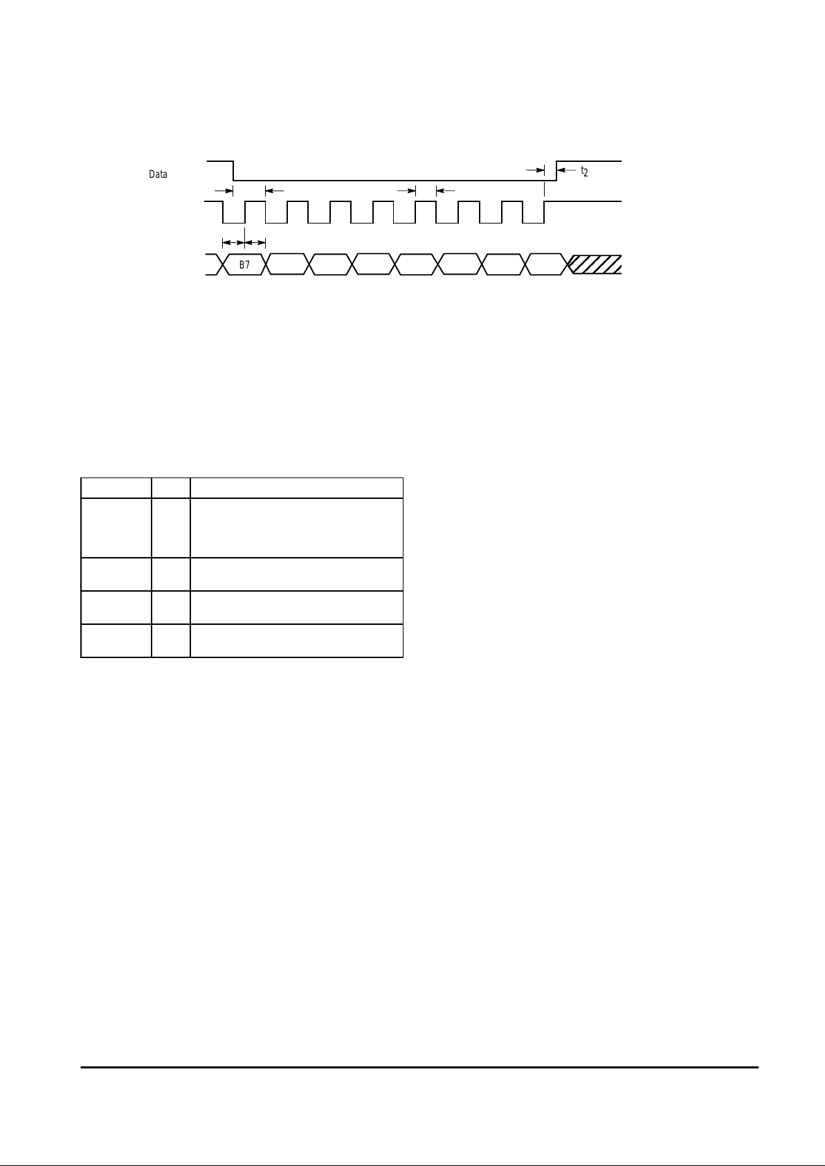
Figure 2. Serial Port Timing Diagram
NOTES: 1. Maximum clock and data rate is 1.0 MHz. There is no required minimum rate.
2.B7 is to be entered first, B0 last.
3.Data is entered on the clock rising edge.
4.Clock can continue to toggle after B0 is entered if Data Ready goes high before the clock’s next rising edge.
This is not recommended due to possible noise problems.
5.Upon power up, all bits are internally set to logic 0, by the POR pin.
6.Data Ready must go low before the first falling clock edge after the clock rising edge associated with B7.
See text for additional information.
B7
t
2
Data Ready
Clock
Data In
t
5
B6 B5 B4 B3 B2 B1 B0
t
1
t3t
4
SERIAL PORT CONTROL BITS
Bits Code Function
B7, B6 00
01
10
11
Normal voice switched operation
Force to receive mode
Force to idle mode
Force to transmit mode
B5 01Attenuator range is 53 dB
Attenuator range is 27 dB
B4 01Microphone amplifier is active
Microphone amplifier is muted
B3–B0
(Note 1)
0000
1111
Maximum receive volume
Minimum receive volume
NOTE: 1. Bit B0 is the LSB for the volume control.
Page 8
MC33218A
8
MOTOROLA ANALOG IC DEVICE DATA
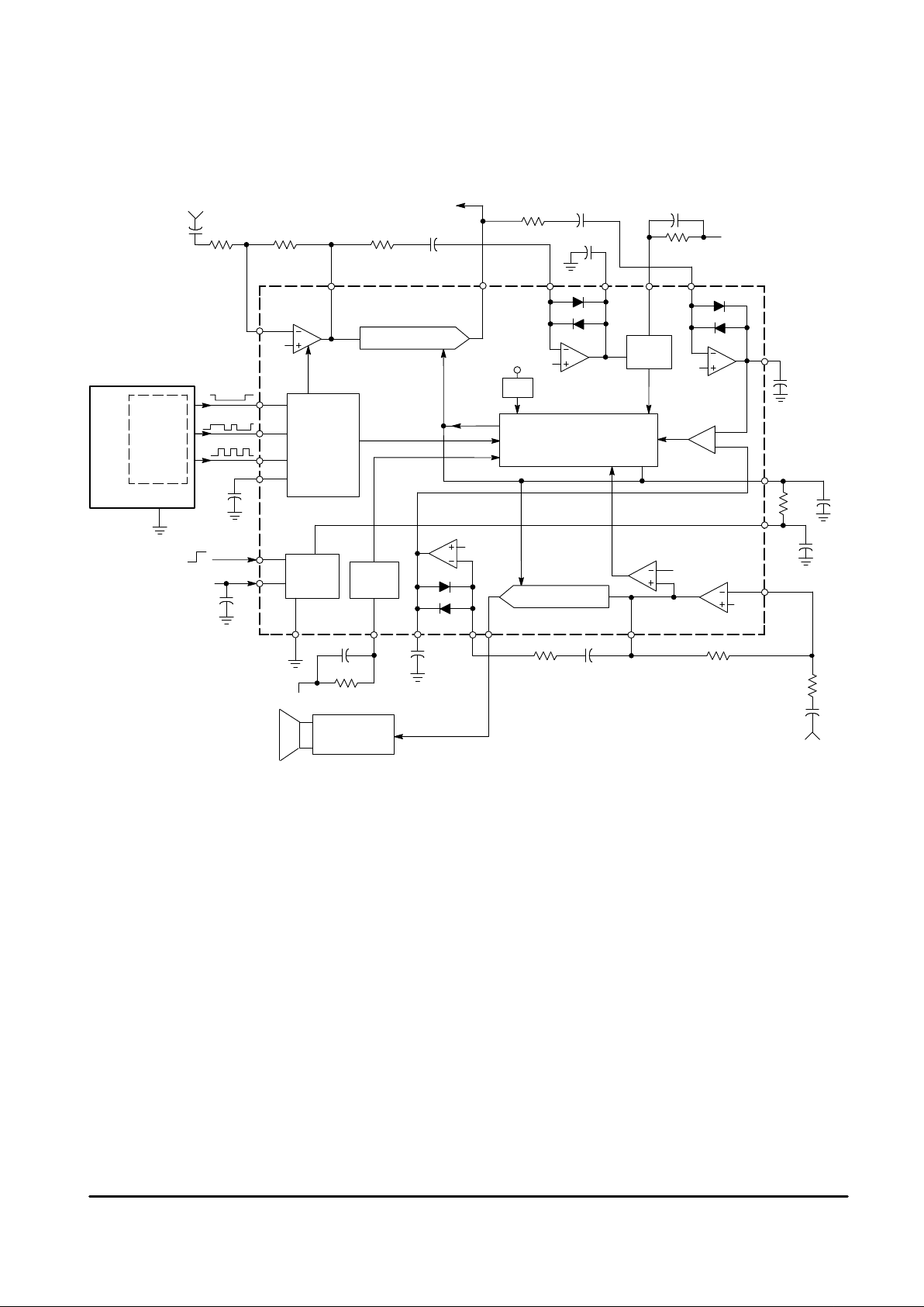
Figure 3. MC33218A Block Diagram and Test Circuit
NOTES: 1. All capacitors are in µF unless otherwise noted.
2.Values shown are suggested initial values only . See Applications Information for circuit adjustments.
MC341 19
Speaker
Amplifier
Receive Input
From 2–4 Wire
Converter
Rx Attenuator
Attenuator Control Circuit
Tx Attenuator
Bias
AGC
T
x
BNM
Dial Tone
Detector
R
x
BNM
0.1
5.1 k
R
2
10 k
10 k
0.1
1.0
47
100 k
V
CC
100
15
15 k
1.0
100
V
B
V
B
V
TH
Microprocessor
DR
Disable
CD
V
CC
0.22
From
Microphone
Transmit Output
To 2–4 Wire Converter
470.14.7 k
0.1
5.1 k
300 k
1.0
100 k
V
CC
VB6
7
5
16
15
14111210
13
24
8
18
21
22
3.0 k
V
B
34
223
1
Tx–Rx Comp.
V
B
V
CC
V
B
Clock
Data
Data
Register
and
Decode
Logic
17
20
19
SPI
Normal
0.1
GND CPR RLO RLI RAO RXO
RXI
CT
TLO
TLICPTCP2TAOMCO XDI
R
1
POR
CK
DIN
DR
MCI
Page 9
MC33218A
9
MOTOROLA ANALOG IC DEVICE DATA
–35
0
–100
10
ATTENUATOR GAIN (dB)
VCT – VB (mV)
ATTENUATOR GAIN (dB)
0–50
50
150100
5.0
8545
0
–10
–20
–30
–40
–10
–20
–30
–40–50
Transmit
Attenuator
Receive
Attenuator
Transmit
Attenuator
Receive
Attenuator
VCT – VB (mV)
0
10
4
8F
C
0
–10
–20
–30
–50
–40
RECEIVE ATTENUATOR GAIN (dB)
VOLUME SETTING (BITS B3–B0, HEX VALUE)
0
10
4
8F
C
0
–10
–20
–30
–50
–40
RECEIVE ATTENUATOR GAIN (dB)
VOLUME SETTING (BITS B3–B0, HEX VALUE)
V
out – B
, OUTPUT VOL TAGE (mV)V
0
100
Vin, INPUT SIGNAL (mVrms)
60
20
0
–60
–20
–100
2.0 µA
V
out
1.0 µF
500
TLI
RLI
XDI
TLO
RLO
CP2
V
in
@ 1.0 kHz
40 80 120 160 200
C
R
2.7
10
2.9
3.1 3.5
3.3
0
–10
–20
–30
–50
–40
RECEIVE ATTENUATOR GAIN (dB)
VCC (Vdc)
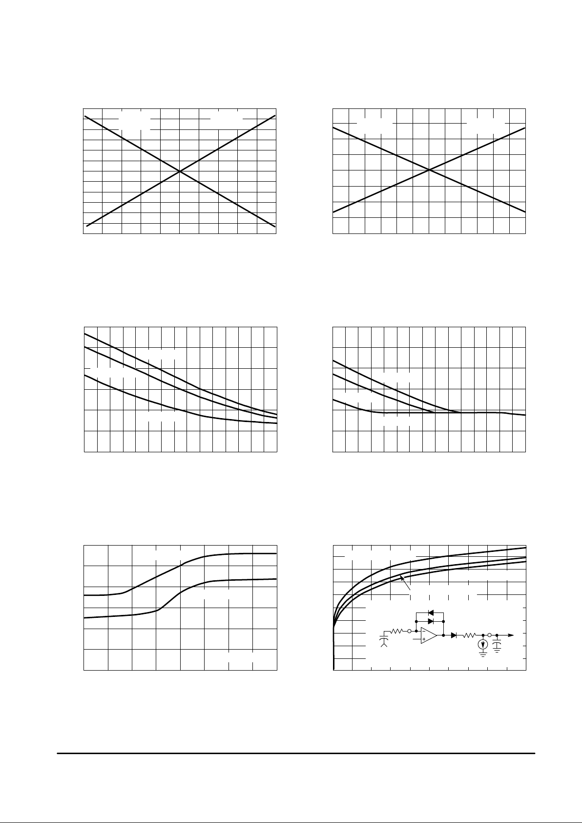
Figure 4. Attenuator Gain versus VCT (Pin 7)
(Full Attenuator Range)
Figure 5. Attenuator Gain versus V
CT
(Half Attenuation Range)
Figure 6. Receive Gain versus Volume Control
Levels (Full Attenuation Range)
Figure 7. Receive Gain versus Volume Control
Levels (Half Attenuation Range)
Figure 8. Receive Gain versus V
CC
Figure 9. Level Detector AC
Transfer Characteristics
–15 25
65
VCC ≥ 3.5 V
VCC = 3.1 V
VCC = 2.7 V
VCC ≥ 3.5 V
VCC = 3.1 V
VCC = 2.7 V
Full Range
Half Range
B3–B0 = 0000
R = 5.1 k, C = 0.1 µF
R = 10 k, C = 0.047 µF
R = 10 k, C = 0.1 µF
V
B
Page 10

MC33218A
10
MOTOROLA ANALOG IC DEVICE DATA
V
out – B
, OUTPUT VOL TAGE (mV)V
100
100
f, FREQUENCY (Hz)
Figure 10. Level Detector AC Transfer
Characteristics versus Frequency
300 1.0 k 10 k
20
–20
60
0
0
200
V
out – B
, OUTPUT VOL TAGE (mV)
Figure 11. Level Detector DC
Transfer Characteristics
100
0
–100
150
50
Iin, DC INPUT CURRENT (
µ
A)
–40 –80 –120 –160 –200
V
INPUT CURRENT ( A)
µ
INPUT VOLTAGE (V)
60
Figure 12. CD Input Characteristics (Pin 8)
40
20
0
0 1.0 2.0 3.0 5.0 7.04.0 6.0
Valid for Vin ≤ V
CC
2.0 µA
V
out
1.0 µF
500
TLI
RLI
XDI
TLO
RLO
CP2
I
in
Figure 13. Power Supply Current
V
B
(V)
0
4.0
0
6.0
IB, OUTPUT CURRENT (mA)
I
CC
(mA)
VCC (V)
Figure 14. VB Output Characteristics
3.0
2.0
1.0
5.0
3.0
2.0
0
– 0.5 –1.0 –1.5
1.0 2.0 3.0 4.0 5.0 6.0
1.0
0
4.0
7.0
200
100
PSRR (dB)
f, FREQUENCY (Hz) at V
CC
Figure 15. VB Power Supply Rejection versus
Frequency and VB Capacitor
80
60
20
0
1.0 k 10 k 20 k
40
2.0 µA
V
out
1.0 µF
500
TLI
RLI
XDI
TLO
RLO
CP2
V
in
@ 1.0 kHz
C
5.1 k
Vin = 100 mVrms
V
B
0.1 µF
–50
V
B
CD ≤ 0.8 V
Idle Mode
2.0 V ≤ CD ≤ V
CC
VCC = 6.5 V
150 µA
VCC = 5.0 V
VCC = 4.0 V
VCC = 3.0 V
–2.0
CVB = 1000 µF
CVB = 100 µF
CVB = 33 µF
Page 11

MC33218A
11
MOTOROLA ANALOG IC DEVICE DATA
2.7 V ≤ VCC ≤6.5 V
2.5
VCC (V)
Figure 16. Receive Amp and Microphone
Amp Output Swing
1.0
0.5
0
3.5 4.5 5.5 6.5
OUTPUT SWING (Vrms)INPUT CURRENT ( A)
µ
0
300
1.0 k
100
INPUT VOLTAGE (V)
∆
GAIN, MUTING (dB)
Figure 17. Microphone Amplifier Muting
versus Feedback Resistor
RF, FEEDBACK RESISTOR (Ω)
Figure 18. Serial Port Input
Characteristics (Pins 17, 18, 19)
80
60
40
20
0
200
100
0
10 k 100 k 300 k
1.0 2.0 3.0 7.05.0 6.04.0
INPUT CURRENT ( A)
µ
0
1000
INPUT VOLTAGE (V)
Figure 19. POR Input Characteristics (Pin 20)
800
600
400
200
–100
1.0 2.0 3.0 7.05.0 6.04.0
RESET TIME (ms)
2.5
80
VCC (V)
Figure 20. Minimum Reset Time versus
VCC and Pin 20 Capacitor
60
40
20
0
3.5 4.5 5.5 6.5
THD = 5%
THD ≤ 1%
THD measured at TAO, RAO
DR
Clk (DR = Hi)
Data & Clk
(DR = Lo)
Valid for Vin ≤ V
CC
VCC = 3.0 V
VCC = 6.5 V
Valid for Vin ≤ V
CC
0
C = 0.68 µF
C = 0.022 µF
C = 0.1 µF
Time for Pin 20 to reach
1.2 V from Ground.
Page 12

MC33218A
12
MOTOROLA ANALOG IC DEVICE DATA
Figure 21. Idle Transmit Timing
MCO
TAO
Output
CPT
C
T
TLO
1.0 s 1.0 s
36 ms
420 mVrms
36 mV
200 mV
140 mV
84 mV
100 mV
240 ms
32 mVrms
85 ms
14 mVrms
200 mVrms, 1.0 kHz
225 ms Time Constant
Idle
T
x
Figure 22. Idle Receive Timing
NOTE: Refer to Figure 3 for component values. Timing and output amplitudes shown are nominal, and are for the indicated input
signal and component values. Actual timing and outputs will vary with the application. Bits B7, B6 = 00.
610 ms
55 ms
360 mV
1.0 s 1.0 s
2.0 mVrms
200 mVrms, 1.0 kHz
225 ms Time Constant
85 ms
150 mV
140 mV
75 ms
RXO
RAO
Output
CPR
C
T
RLO
420 mVrms
Idle
R
x
Page 13
MC33218A
13
MOTOROLA ANALOG IC DEVICE DATA
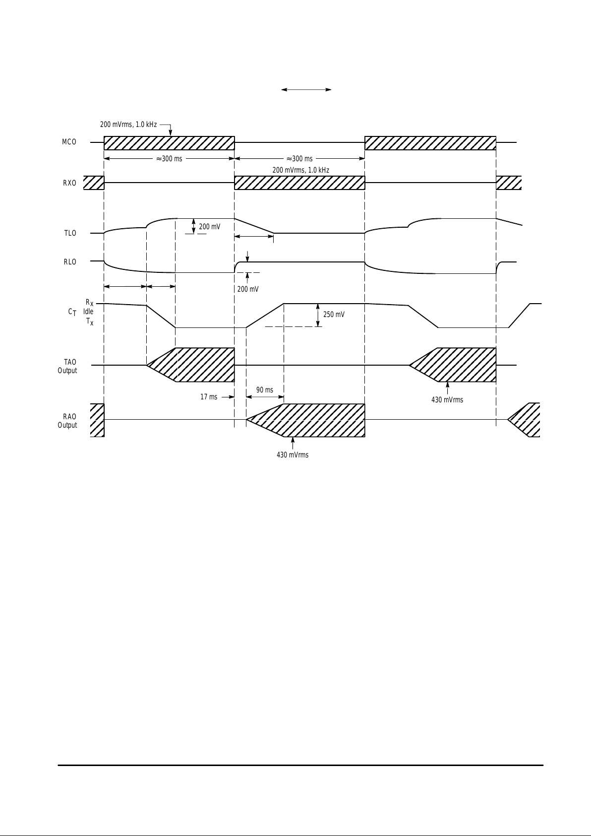
Figure 23. Transmit Receive Timing
(Short Cycle Timing)
NOTE: External component values are those shown in Figure 3. Timing and output amplitudes shown are nominal, and are for the
indicated input signal and component values. Actual timing and outputs will vary with the application. Bits B7, B6 = 00.
80 ms 75 ms
100 ms
≈
300 ms
200 mVrms, 1.0 kHz
≈
300 ms
200 mVrms, 1.0 kHz
200 mV
200 mV
250 mV
430 mVrms
430 mVrms
90 ms
17 ms
MCO
TAO
Output
Idle
T
x
RXO
TLO
RLO
C
T
RAO
Output
R
x
Page 14

MC33218A
14
MOTOROLA ANALOG IC DEVICE DATA
Figure 24. Transmit Receive Timing
(Long Cycle Timing)
ÎÎÎÎ
ÎÎÎÎ
≈
1.0 s
200 mVrms, 1.0 kHz
≈
1.0 s
200 mVrms, 1.0 kHz
200 mV
200 mV
250 mV
85 ms
75 ms
145 ms
80 ms
430 mVrms
430 mVrms
67 mVrms
t1
225 ms Time Constant
MCO
TAO
Output
Idle
T
x
RXO
TLO
RLO
C
T
RAO
Output
R
x
NOTE: External component values are those shown in Figure 3. Timing and output amplitudes shown are nominal, and are for the
indicated input signal and component values. Actual timing and outputs will vary with the application. Time t1 depends on
the ratio of the “on”/“off” amplitude of the signal at MCO. Bits B7, B6 = 00.
Page 15

MC33218A
15
MOTOROLA ANALOG IC DEVICE DATA
Figure 25. Transmit Receive Timing
(Long Cycle Timing)
NOTE: External component values are those shown in Figure 3, except the capacitor at CT is 6.8 µF . Timing and output amplitudes
shown are nominal, and are for the indicated input signal and component values. Actual timing and outputs will vary with the
application. Time t1 depends on the ratio of the “on”/“off” amplitude of the signal at MCO. Bits B7, B6 = 00.
ÎÎÎÎ
ÎÎÎÎ
≈
1.0 s
200 mVrms, 1.0 kHz
≈
1.0 s
200 mVrms, 1.0 kHz
200 mV
200 mV
250 mV
85 ms
27 ms
83 ms
29 ms
430 mVrms
430 mVrms
40 mVrms
t1
100 ms Time Constant
MCO
TAO
Output
Idle
T
x
RXO
TLO
RLO
C
T
RAO
Output
R
x
Page 16

MC33218A
16
MOTOROLA ANALOG IC DEVICE DATA
Figure 26. Chip Disable Timing
Figure 27. Mute Timing
Figure 28. POR Timing
NOTE: Above time established by first muting the microphone amplifier (B4 = 1). Then the POR pin is taken low. The 30 µs is representative
if the internal delay for the internal registers to be reset to 0, and the associated function change. The registers will remain set to 0
when POR goes high, until new data is written.
t1
t
off
3.0 µs
5.0 µs
CD Input
(Pin 8)
Output at
RAO, TAO
t
off
10 ms
20 ms
≥
50 ms
t1
25 ms
45 ms
60 ms
2.0 µs 1.0 µs
B4 = 1 B4 = 0
Data Ready
(Pin 19)
Output at
MCO
1.2 V
MCO
30 µs
POR
(Pin 20)
NOTE: Enable time t1 depends on the length of t
off
according to the following chart:
Page 17

MC33218A
17
MOTOROLA ANALOG IC DEVICE DATA
FUNCTIONAL DESCRIPTION
Introduction
The fundamental difference between the operation of a
speakerphone and a telephone handset is that of half–duplex
versus full–duplex. The handset is full duplex, meaning
conversation can occur in both directions (transmit and
receive) simultaneously. This is possible due to both the low
sound level at the receiver, and the fact that the acoustic
coupling from the earpiece to the mouthpiece is almost
non–existent (the receiver is normally held against a person’s
ear). The loop gain from the receiver to the microphone and
through the circuit is well below that needed to sustain
oscillations.
A speakerphone, on the other hand, has higher gain levels
in both the transmit and receive paths, and attempting to
converse full duplex results in oscillatory problems due to the
loop that exists within the speakerphone circuit. The loop is
formed by the hybrid, the acoustic coupling (speaker to
microphone), and the transmit and receive paths (between
the hybrid and the speaker/microphone). The only practical
and economical method used to date is to design the
speakerphone to function in a half duplex mode –
i.e., only
one person speaks at a time, while the other listens. To
achieve this requires a circuit which can detect who is talking
(in reality, who is talking louder), switch “on” the appropriate
path (transmit or receive), and switch “off” (attenuate) the
other path. In this way, the loop gain is maintained less than
unity. When the talkers exchange function, the circuit must
quickly detect this, and switch the circuit appropriately. By
providing speech level detectors, the circuit operates in a
“hands–free” mode, eliminating the need for a “push–to–talk”
switch.
The MC33218A provides the necessary circuitry to perform
a voice switched, half duplex, speakerphone function. The IC
includes transmit and receive attenuators, pre–amplifiers, and
level detectors and background noise monitors for each path.
An attenuator control circuit automatically adjusts the gain of
the transmit and receive attenuators based on the relative
strengths of the voice signals present, the volume control, and
the supply voltage (when low). The detection sensitivity and
timing are externally controllable.
The MC33218A is unique compared to most
speakerphone integrated circuits in that it has a
microprocessor serial port for control of various functions.
Those functions are:
– Volume level (15 steps of ≈ 3.0 dB each)
– Microphone amplifier mute
– Attenuator range selection (53 dB or 27 dB)
– Force to receive, idle, or transmit to override the
automatic switching.
Please refer to the Block Diagram (Figure 3) when reading
the following sections.
Transmit and Receive Attenuators (Full Range B5 = 0)
The transmit and receive attenuators are complementary,
performing a log–antilog function. When one is at maximum
gain (≈ 6.7 dB), the other is at maximum attenuation
(– 47 dB) – they are never both fully “on” or fully “off”. Both
attenuators are controlled by a single output from the
Attenuator Control Circuit which ensures the sum of their
gains will remain constant at a typical value of –40 dB. Their
purpose is to provide the half–duplex operation required in a
speakerphone.
The attenuators are non–inverting, and have a usable
bandwidth of 50 kHz. Their input signal (at MCO and RXO)
should be limited to 300 mVrms (850 mVp–p) to prevent
distortion. That maximum recommended input signal is
independent of the volume control setting. Both the inputs and
outputs are biased at ≈ VB. The output impedance is <10 Ω
until the output current limit (typically 2.0 mA peak) is reached.
The attenuators are controlled by the single output of the
Attenuator Control Circuit, which is measurable at CT (Pin 7).
When the circuit detects speech signals directing it to the
receive mode (by means of the level detectors described
below), an internal current source of 42 µA will charge the C
T
capacitor to a voltage positive with respect to VB (see
Figure 29). At the maximum volume control setting, this
voltage will be approximately +150 mV, and the receive
attenuator will have a gain of +6.7 dB. When the circuit
detects speech signals directing it to the transmit mode, an
internal current source of 42 µA will take the capacitor to
approximately –100 mV with respect to VB (the transmit
attenuator will have a gain of + 6.7 dB). When there is no
speech present in either path, the current sources are shut
off, and the voltage at CT will decay to be equal to VB. This is
the idle mode, and the attenuators’ gains are nearly half–way
between their fully “on” and fully “off” positions (– 25 dB for
the Rx attenuator, –16 dB for the Tx attenuator). Monitoring
the CT voltage (with respect to VB) is the most direct method
of monitoring the circuit’s mode, and its response.
Transmit and Receive Attenuators (Half Range B5 = 1)
With the attenuators set to the half range, the attenuator
which is “on” will have a gain of ≈ –7.0 dB, while the “off”
attenuator will have a gain of ≈ –34 dB. The idle mode is the
same as for the full range (– 25 dB for the Rx attenuator,
–16 dB for the Tx attenuator). The voltage at the CT pin, with
respect to VB, will be – 35 mV for the transmit mode, and
+85 mV for the receive mode.
Attenuator Control Circuit
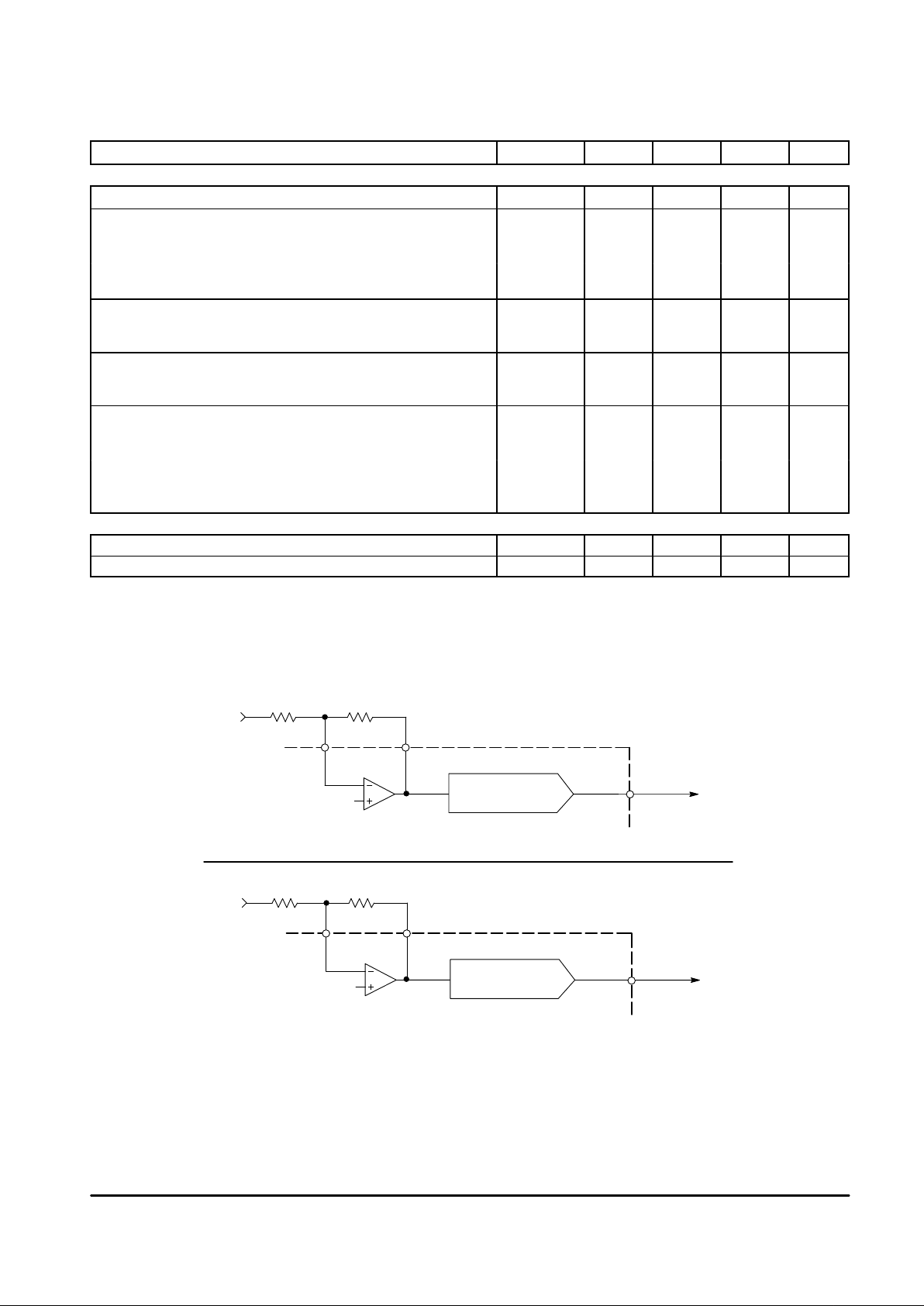
The inputs to the Attenuator Control Section (Figure 29)
are six: The T
x
–R
x
comparator operated by the level
detectors, two background noise monitors, the AGC circuit,
the dial–tone detector, and the microprocessor interface.
These six functions are described as follows.
Level Detectors, T
x
–R
x
Comparator
There are two identical level detectors – one on the
receive side and one on the transmit side (refer to Figure 30).
Each level detector is a high gain amplifier with
back–to–back diodes in the feedback path, resulting in
non–linear gain, which permits operation over a wide
dynamic range of speech levels. Refer to the graphs of
Figures 9, 10, and 11 for their DC and AC transfer
characteristics. The sensitivity of each level detector is
determined by the external resistor and capacitor at their
input (TLI and RLI). The output charges an external capacitor
through a diode and limiting resistor, thus providing a DC
representation of the input AC signal level. The outputs have
a quick rise time (determined by the capacitor and an internal
500 Ω resistor), and a slow decay time set by an internal
current source and the capacitor. The capacitors at RLO and
TLO should have the same value (±10%) to prevent timing
problems.
Page 18

MC33218A
18
MOTOROLA ANALOG IC DEVICE DATA
Figure 29. CT Attenuator Control Circuit
V
B
I
1
42
µ
A
To
Attenuators
R
T
C
T
Background
Monitors
T
x
–
Rx Comp
µ
P Interface
Dial Tone Det.
Voltage Clamps
Control Circuit
I
2
42
µ
A
C
T
MC33218A
AGC
T
x
R
x
R
x
T
x
Referring to Figure 3, the outputs of the two level detectors
drive the T
x
–R
x
comparator. The comparator’s output state
depends on whether the transmit or receive speech signal is
stronger, as sensed by the level detectors. The Attenuator
Control Circuit uses this signal, along with the background
noise monitors, to determine which mode to set.
Figure 30. Level Detector
TLO
(RLO)
1.0
µ
F
500
Ω
2.0 µA
TLI
(RLI)
V
B
R
C
Signal
Input
External Component Values are
Application Dependent.
Background Noise Monitors
The purpose of a background noise monitor is to
distinguish speech (which consists of bursts) from
background noise (a relatively constant signal). There are
two background noise monitors
– one for the receive path and
one for the transmit path. Referring to Figure 32, each is
operated on by a level detector, which provides a dc voltage
representative of the combined speech and noise level. The
peaks, valleys, and bursts, which are characteristic of
speech, will cause that DC voltage (at CP2 or RLO) to
increase relatively quickly, causing the output of the next
amplifier to also rise quickly. If that increase exceeds the
36 mV offset, at a speed faster than the time constant at CPT
(CPR), the output of the last comparator will change,
indicating the presence of speech to the attenuator control
circuit. This will keep the circuit in either the transmit or the
receive mode, depending on which side has the stronger
signals. Whenever a new continuous signal is applied, the
time constant at CPT (CPR) determines how long it takes the
circuit to decide that the new sound is continuous, and
therefore background noise. The system requires that the
average speech signal be stronger than the background
noise level (by 6.0–7.0 dB) for proper speech detection to
occur.
When only background noise is present in both paths, the
output of the monitors will indicate the absence of speech,
allowing the circuit to go to the idle mode.
AGC Circuit
In the receive mode only, the AGC circuit decreases the
gain of the receive attenuator when the supply voltage at V
CC
falls below 3.5 V , according to the graph of Figure 8. The gain
of the transmit path changes in a complementary manner.
The purpose of this feature is to reduce the power (and
current) used by the speaker when the speakerphone is
powered by the phone line, and is connected to a long
telephone line, where the available power is limited.
Reducing the speaker power controls the voltage sag at V
CC,
reduces clipping and distortion at the speaker output, and
prevents possible erratic operation.
Dial Tone Detector
When a speakerphone is initially taken off–hook, the dial
tone signal will switch the circuit to the receive mode.
However, since the dial tone is a continuous signal, the
MC33218A will consider it as background noise, rather than
speech, and would switch from receive to idle, causing the
dial tone sound to fade. The dial tone detector prevents the
fading by disabling the receive background noise monitor.
The dial tone detector is a comparator with one side
connected to the receive attenuator input (RXO), and the other
input connected to VB with a –20 mV offset (see Figure 31). If
the circuit is in the receive mode, and the incoming signal has
peaks greater than 20 mV (14 mV rms), the comparator’s
output will change, keeping the circuit from switching to the
idle mode. The receive attenuator will then be at a gain
determined solely by the volume control. NOTE: The dial tone
detector is not a frequency discriminating circuit.
Figure 31. Dial Tone Detector
T o Attenuator
Control Circuit
To Rx
Attenuator
V
B
20 mV
RXO
Page 19

MC33218A
19
MOTOROLA ANALOG IC DEVICE DATA
Figure 32. Background Noise Monitor
18.6 k
500
Ω
XDI
(RLI)
V
B
R
C
Signal
Input
31.7 k
V
B
CP2
(RLO)
CPT
(CPR)
2.0
µ
A
36 mV
47
µ
F
100 k
T o Attenuator
Control Circuit
Background
Noise Monitor
V
CC
1.0
µ
F
External Component Values are
Application Dependent.
Microprocessor Interface
The three line SPI port (Pins 17–19) is used for setting
various functions with a single 8 bit word. The functions are
as follows:
– Volume Control: Bits B0–B3 control the gain of the
attenuators only when in the receive mode. Setting
B3–B0 = 0000 sets the receive attenuator to its maximum gain
(+ 6.7 dB in full range, –7.0 dB in half range), and therefore
maximum volume at the speaker. Setting B3–B0 = 1111 sets
the receive attenuator to a minimum gain level (≈ –32 dB), and
is the minimum volume setting. B0 is the LSB for this function,
and each step changes the gain by ≈ 3.0 dB at the high
volume end (see Figure 6 and 7). The transmit attenuator gain
is varied in a complementary manner. These bits have no
effect in the idle or transmit modes.
– Muting of the Microphone Amplifier: Bit B4 is used to set
the microphone amplifier to the normal or the muted mode.
When this bit is a 1, the amplifier is muted. See the paragraph
entitled “Microphone Amplifier, Mute” elsewhere in this
document.
– Attenuator Range: Bit B5 is used to select the attenuator
range. When it is a 0, the range is 53 dB (from full “on” to full
“off”). When it is a 1, the range is 27 dB. The 53 dB range is
used for the majority of applications, such as desktop
speakerphones (home or office use), intercom units, and any
application where the speaker and microphone are in close
proximity. The 27 dB range is commonly used in European
speakerphone applications, where the typical design
involves using the handset for the microphone function, and
is therefore somewhat separated from the speaker.
– Operating Mode: Bits B7 and B6 set the circuit operating
mode. When 00, the normal voice activated switching is
enabled, and the circuit responds to the speech levels as
described elsewhere in this document. When 01, the circuit is
forced to the receive mode in that the receive attenuator is
“on” and the transmit attenuator is “off”. The volume control
(Bits B3–B0) is effective in this mode. When 10, the circuit is
forced to the idle mode. When 11, the circuit is forced to the
transmit mode. The volume control bits have no effect in the
idle or transmit modes.
The eight bits are entered serially, B7 first and B0 last.
Each bit is entered on a clock rising edge. The maximum
clock and data rate is 1.0 MHz, and there is no minimum
required speed. Data Ready, which is normally high, is to be
held low while the eight bits are clocked in. The eight bits take
effect when Data Ready is taken high. There is no chip
address, or other protocol or handshaking required. See
Figure 2 for a timing diagram. Note that Data Ready need not
be taken low before the first clock rising edge. It must be
taken low before the first clock falling edge which follows the
first clock rising edge. This allows Data Ready to be taken
low coincident with the first clock rising edge, if desired, as
well as before that.
It is recommended that DR be kept high when not entering
data, to prevent disruption of the circuit by transients or
glitches on the clock or data lines. This is not required, and
DR may be taken low after latching in data, if desired.
The clock input can be stopped after B0 is entered, or it
may continue to run as long as Data Ready is taken high
before the next clock rising edge. It is recommended that the
clock not be continued to prevent possible noise problems.
The three inputs must be kept within the range of VCC and
GND. If an input is taken more than 0.5 V above VCC or below
GND excessive currents will flow, and the device’s operation
will be distorted. See Figure 18 for input current requirements
at these pins.
Power On Reset
The Power On Reset, when at a logic low (below its
threshold of 1.2 V) resets the internal registers to a logic 0,
independent of the Clock, Data, or Data Ready position. A
capacitor on this pin provides a power up time delay to allow
VCC to stabilize before the registers can accept data.
Alternately, Pin 20 can be driven directly from a logic source
if desired. The POR input must be kept within the range of
VCC and GND. If the input is taken more than 0.5 V above
VCC or below GND excessive currents will flow, and the
device’s operation will be distorted. The configuration of this
pin is shown in Figure 33.
When VCC is applied to the MC33218A, the registers will
be enabled when the voltage at POR exceeds 1.2 V . The time
to reach this level depends on the capacitor at POR, and
VCC, and will not be less than the time shown in Figure 20.
The actual reset time is affected by the rise time of VCC. Any
data written to the registers while POR is below 1.2 V will not
be stored or effective.
The nominal DC voltage at POR is ≈ 1.5 V.
The registers may be intentionally reset by external control
by pulling POR to ground with (for example) an open collector
NPN transistor. The time to reset is shown in Figure 28. When
POR once again goes high, the registers’ data will remain at 0
until new data is entered. Old data is not retained. The time
required to release the registers after releasing POR (by
turning “off” the NPN transistor) is shown in Figure 20.
Page 20

MC33218A
20
MOTOROLA ANALOG IC DEVICE DATA
If POR is driven by an external logic output, its input
current requirement is shown in Figure 19.
Figure 33. Power On Reset Pin
V
CC
5.0 k
POR
CD
96 k
Microphone Amplifier, Mute
The microphone amplifier (Pins 21, 22) has the
non–inverting input internally connected to VB, while the
inverting input and the output are pinned out. Unlike most
op–amps, the amplifier has an all–NPN output stage, which
maximizes phase margin and gain–bandwidth. This feature
ensures stability at gains less than unity, as well as with a
wide range of reactive loads. The open loop gain is typically
80 dB (f <100 Hz), and the gain–bandwidth is typically
1.5 MHz. The maximum output swing, for 1.0% or less
distortion, is determined by the input capability of the transmit
attenuator (300–350 mVrms), and by VCC at low supply
voltages (see Figure 16). The output impedance is <10 Ω
until current limiting is reached (typically 2.0 mA peak). The
input bias current at MCI is typically 30 nA out of the pin.
The mute function, when activated, will reduce the gain of
the amplifier by shorting the external feedback resistor (RMF
Figure 34). The amplifier is not disabled in this mode – MCO
remains a low impedance output, and MCI remains a virtual
ground at VB. The amount of muting (the change in gain)
depends on the value of the external feedback resistor,
according to the graph of Figure 17. Muting is enabled by
setting bit B4 to a logic 1.
Figure 34. Microphone Amplifier and Mute
V
B
R
MI
From
Microphone
From
µ
P
R
MF
MCO
MCI
µ
P Interface
B4
Receive Amplifier
The receive amplifier (Pins 15, 16) has the non–inverting
input internally connected to VB, while the inverting input and
the output are pinned out. Unlike most op–amps, the
amplifier has an all–NPN output stage, which maximizes
phase margin and gain–bandwidth. This feature ensures
stability at gains less than unity, as well as with a wide range
of reactive loads. The open loop gain is typically 80 dB
(f <100 Hz), and the gain–bandwidth is typically 1.5 MHz.
The maximum p–p output swing, for 1.0% or less distortion, is
determined by the input capability of the receive attenuator
(300–350 mVrms), and by VCC at low supply voltages (see
Figure 16). The output impedance is <10 Ω until current
limiting is reached (typically 2.0 mA peak). The input bias
current at RXI is typically 30 nA out of the pin.
Power Supply, VB and Chip Disable
The power supply voltage at Pin 24 is to be between 3.5
and 6.5 V for normal operation, and down to 2.7 V with the
AGC in effect (see AGC section). The supply current required
is typically 4.6 mA in the idle and transmit modes (at 5.0 V),
and slightly more in the receive mode. Figure 13 shows the
supply current for both the normal and disabled modes.
The output voltage at VB (Pin 6) is approximately equal to
(VCC – 0.7)/2, and provides an ac ground for the internal
amplifiers, and the system. The output impedance at VB is
approximately 600 Ω, and in conjunction with the external
capacitor at VB, forms a low pass filter for power supply noise
rejection. The choice of the VB capacitor size is application
dependent based on whether the circuit is powered by the
telephone line or a regulated supply . See Figure 15 for PSRR
data from VCC to VB. Since VB biases the microphone and
receive amplifiers, the amount of supply rejection at their
outputs is a function of the rejection at VB, as well as the
gains of the amplifiers.
The amount of current which can be sourced out of the V
B
pin depends on the VCC voltage (see Figure 14). Drawing
current in excess of that shown in Figure 14 will cause VB to
drop low enough to disrupt the circuit’s operation. This pin
can sink ≈ 100 µA when enabled, and 0 µA when disabled.
The Chip Disable (Pin 8) permits powering down the IC for
power conservation. With CD between 0 and 0.8 V, normal
operation is in effect. With CD between 2.0 V and VCC, the IC
is powered down, and the supply current drops to ≈ 11 0 µA
(at VCC = 5.0 V, see Figure 13). When CD is high, the
microphone and receive amplifiers, the level detectors, and
the two attenuators are disabled (their outputs go to a high
impedance). The background noise monitors are disabled,
and Pins 3 and 10 will go to VCC. The VB output, however,
remains active, except that it cannot sink any current. The
serial port is disabled so that new data may not be entered.
Upon re–enabling the circuit, the 8 internal registers will be
set to 0, regardless of their previous contents. Figure 26
indicates the disable and enable timing.
The CD input must be kept within the range of VCC and
GND. See Figure 12 for input current requirements. If the
input is taken more than 0.5 V above VCC or below GND,
excessive currents will flow, and the device’s operation will
be distorted. If the disable function is not used, the pin should
be connected to ground.
Page 21

MC33218A
21
MOTOROLA ANALOG IC DEVICE DATA
APPLICATIONS INFORMATION
Switching and Response Time Theory
The switching time of the MC33218A circuit is dominated
by the components at CT (Pin 7, refer to Figure 3), and
second by the capacitors at the level detector outputs (RLO,
TLO).
The transition time to receive or to transmit mode from
idle, or from the other mode, is determined by the capacitor at
CT, together with the internal current sources (refer to
Figure 29). The switching time is:
DT+
DV
C
T
I
When switching from idle to receive, ∆V = 150 mV,
I = 42 µA, the CT capacitor is 15 µF, and ∆T calculates to
≈ 53 ms. When switching from idle to transmit, ∆V = 100 mV,
I = 42 µA, the CT capacitor is 15 µF, and ∆T calculates to
≈ 36 ms.
When the circuit switches to idle, the internal current
sources are shut “off”, and the time constant is determined by
the CT capacitor and RT, the external resistor (see
Figure 29). With CT = 15 µF, and RT = 15 kΩ, the time
constant is ≈ 225 ms, giving a total switching time of ≈ 0.68 s
(for 95% change). The switching period to idle begins when
both speakers have stopped talking. The switching time back
to the original mode will depend on how soon that speaker
begins speaking again. The sooner the speaking starts
during the “decay to idle” period, the quicker the switching
time since a smaller voltage excursion is required. That
switching time is determined by the internal current sources
as described above.
When the circuit switches directly from receive to transmit
(or vice–versa), the total switching time depends not only on
the components and currents at the CT pin, but also on the
response of the level detectors, the relative amplitude of the
two speech signals, and the mode of the circuit, since the two
level detectors are connected differently to the two
attenuators.
The rise time of the level detector’s outputs (RLO, TLO) is
not significant since it is so short. The decay time, however,
provides a significant part of the “hold time” necessary to hold
the circuit (in transmit or receive) during the normal pauses in
speech. The capacitors at the two outputs must be equal
value (±10%) to prevent problems in timing and signal
response.
The components at the inputs of the level detectors (RLI,
TLI) do not affect the switching time, but rather affect the
relative signal levels required to switch the circuit, as well as
the frequency response of the detectors. They must be
adjusted for proper switching response as described later in
this document.
Switching and Response Time Measurements
Using burst of 1.0 kHz sine waves to force the circuit to
switch among its modes, the timing results were measured
and are indicated in Figures 21–25.
a) In Figure 21, when a signal is applied to the transmit
attenuator only (normally via the microphone and the
microphone amplifier), the transmit background noise
monitor immediately indicates the “presence of speech” as
evidenced by the fact that CPT begins rising. The slope of the
rising CPT signal is determined by the external resistor and
capacitor on that pin. Even though the transmit attenuator is
initially in the idle mode (–16 dB), there is sufficient signal at
its output to cause TLO to increase. The attenuator control
circuit then forces the circuit to the transmit mode, evidenced
by the change at the CT pin. The attenuator output signal is
then 6.7 dB above the input.
With the steady sine wave applied to the transmit input,
the circuit will stay in the transmit mode until the CPT pin gets
to within 36 mV of its final value. At that point the internal
comparator (see Figure 32) switches, indicating to the
attenuator control circuit that the signal is not speech, but
rather it is background noise. The circuit now begins to decay
to idle, as evidenced by the change at CT and TLO, and the
change in amplitude at TAO.
When the transmit signal at MCO is removed (or reduced),
the CPT pin drops quickly, allowing the CPT to quickly
respond to any new speech which may appear afterwards.
The voltage at CT decays according to the time constant of its
external components, if not already at idle.
The voltage change at CP2, CPT, and TAO depend on the
input signal’s amplitude, and the components at XDI and TLI.
The change at CT is internally fixed at the level shown. The
timing numbers shown depend both on the signal amplitudes
and the components at the CT and CPT pins.
b) Figure 22 indicates what happens when the same
signal is applied to the receive side only. RLO and CPR react
similarly to TLO and CPT. However, the circuit does not
switch to idle when CPR finishes transitioning since the dial
tone detector disables the background noise monitor,
allowing the circuit to stay in the receive mode as long as
there is a signal present. If the input signal amplitude had
been less than the dial tone detector’s threshold, the circuit
response would have been similar to that shown in Figure 21.
The voltage change at CT depends on the setting of the
volume control (bits B3–B0). The +150 mV represent
maximum volume.
c) Figure 23 indicates the circuit response when transmit
and receive signals are alternately applied, with relatively
short cycle times (300 ms each) so that neither attenuator will
begin to go to idle during its “on” time. Figure 24 indicates the
circuit response with longer cycle times (1 s each), where the
transmit side is allowed to go to idle. Figure 25 is the same as
Figure 24, except the capacitor at CT has been reduced from
15 µF to 6.8 µF, providing a quicker switching time. The
reactions at the various pins are shown. The response times
at TAO and RAO are different, and typically slightly longer
than what is shown in Figures 21 and 22 due to:
– The larger transition required at CT pin,
– The greater difference in the levels at RLO and TLO due
to the positions of the attenuators, as well as their decay time,
and
– Response time of background noise monitors.
The timing responses shown in these three figures are
representative for those input signal amplitudes, and burst
durations. Actual response time will vary for different signal
conditions.
NOTE: While it may seem desirable to decrease the
switching time between modes by reducing the capacitor at
CT, this should be done with caution for two reasons:
1) If the switching time is too short, the circuit response
may appear to be “too quick” to the user, who may consider
its operation erratic. The recommended values in this data
sheet, along with the accompanying timings, provide what
Page 22

MC33218A
22
MOTOROLA ANALOG IC DEVICE DATA
experience has shown to be a “comfortable response“ by the
circuit.
2) The distortion in the receive attenuator will increase as
the CT capacitor value is decreased. The extra THD will be
most noticeable at the lower frequencies, and at the lower
amplitudes. Table 1 provides a guideline for this issue.
Table 1. THD versus CT Capacitor
CT
Capacitor
Idle–R
x
Transition
Input
@ RAI
Freq.
THD
@ RAO
15 µF 53 ms 20 mVrms
300 Hz 1.5%
1.0 kHz 0.3%
100 mVrms
300 Hz 0.6%
1.0 kHz 0.12%
6.8 µF 24 ms 20 mVrms
300 Hz 3.6%
1.0 kHz 1.0%
100 mVrms
300 Hz 1.4%
1.0 kHz 0.4%
3.3 µF 12 ms 20 mVrms
300 Hz 7.0%
1.0 kHz 1.9%
100 mVrms
300 Hz 2.8%
1.0 kHz 0.7%
Considerations in the Design of a Speakerphone
The design and adjustment of a speakerphone involves
human interfaces issues, as well as proper signal levels.
Because of this fact, it is not practical to do all of the design
mathematically. Certain parts of the design must be done by
trial and error, most notably the switching response and the
“How does it sound?” part of the testing. Among the
recommendations for a successful design are:
1) Design the enclosure concurrently with the
electronics. Do not leave the case design to the end as its
properties are just as important (just as
equally
important) as
the electronics. One of the major issues involved in a
speakerphone design is the acoustic coupling of the speaker
to the microphone, which must be minimized. This parameter
is dependent entirely on the design of the enclosure, the
mounting of the speaker and the microphone, and their
characteristics.
2) Ensure the speaker is optimally mounted. This fact
alone can make a difference of several dB in the sound level
from the speaker, as well as the sound quality. The speaker
manufacturer should be consulted for this information.
3) Do not breadboard the circuit with the microphone and
speaker hanging out in midair. It will not work. The speaker
and microphone must be in a suitable enclosure, preferably
one resembling the end product. If this is not feasible,
temporarily use some other properly designed enclosure,
such as one of the many speakerphones on the market.
4) Do not breadboard the circuit on a wirewrapped board
or a plug–in prototyping board. Use a PC board, preferably
with a ground plane. Proper filtering of the supply voltage, at
the VCC pin, is essential.
5) The speakerphone must be tested with the intended
hybrid, and connected to a phone line, or phone line
simulator. The performance of the hybrid is just as important
as the enclosure and the speakerphone IC.
6) When testing the speakerphone, be conscious of the
environment. If the speakerphone is in a room with large
windows and tile floors, it will sound different than if it is in a
carpeted room with drapes. Additionally, be conscious of the
background noise in a room.
7) When testing the speakerphone on a phone line, make
sure the person at the other end of the phone line is not in the
same room as the speakerphone.
Design and Adjustment Procedure
Assuming the end product enclosure is available, with the
intended production microphone and speaker installed, and
the PC boards installed (or temporary substitutes for the PC
boards) a recommended sequence is as follows (refer to
Figure 35):
1) Design the hybrid, ensuring it interfaces properly with
the phone line for both DC and AC characteristics. The return
loss must be adjusted so as to comply with the appropriate
regulatory agency. The sidetone should then be adjusted
according to the intent of the product. If the product is a
speakerphone only, without a handset, the sidetone gain
(GST) should be adjusted for maximum loss. If a handset is
part of the end product, the sidetone must be adjusted for the
minimum acceptable sidetone levels in the handset.
Generally, for the speakerphone, 10–20 dB sidetone loss is
preferred for GST.
2) Check the acoustic coupling of the enclosure (GAC in
Figure 35). With a steady sound coming out of the speaker,
measure the rms voltage on the speaker terminals, and the
rms voltage out of the microphone. Experience has shown
that the loss should be at least 40 dB, preferably 50 dB. This
should be checked over the frequency range of 20 Hz to
10 kHz.
3) Adjust the transmit path for proper signal levels, based
on the lowest speech levels as well as the loudest. Based on
the typical levels from commonly available microphones, a
gain of about 35–45 dB is required from the microphone
terminals to Tip and Ring. Most of that gain should be in the
microphone amplifier so as to make best use of the transmit
attenuator, but make sure the maximum attenuator input
level at MCO is not exceeded. If a signal generator is used
instead of a microphone for testing, the circuit can be locked
into the transmit mode by grounding CPT (Pin 3), or using
bits B7 and B6 (set to 11). Frequency response can generally
be tailored with capacitors at the microphone amplifier.
4) Adjust the receive path for proper signal levels, based
on the lowest speech levels as well as the loudest. A gain of
about 30 dB is required from Tip and Ring to the speaker
terminals for most applications (at max. volume). Most of that
gain should be in the receive amplifier (at RXI, RXO) so as to
make best use of the receive attenuator, but make sure the
max. attenuator input level at RXO is not exceeded. If a
signal generator is used for signal injection during testing, the
circuit can be locked into the receive mode by grounding
CPR (Pin 10), although this is usually not necessary since
the dial tone detector will keep the circuit in the receive mode.
As an alternate, bits B7 and B6 can be set to 01. Frequency
response can generally be tailored with capacitors at the
receive amplifier.
5) Check that the loop gain (i.e., the receive path gain +
acoustic coupling gain + transmit path gain + sidetone gain)
is less than 0 dB over all frequencies. If not, “singing” will
occur – a steady oscillation at some audible frequency.
6) a) The final step is to adjust the resistors at the level
detector inputs (RLI and TLI) for proper switching response
Page 23

MC33218A
23
MOTOROLA ANALOG IC DEVICE DATA
(the switchpoint occurs when I1 = I2). This has to be the last
step as the resistor values depend on all of the above
adjustments, which are based on the mechanical, as well as
the electrical, characteristics of the system. NOTE: An
extreme case of level detector misadjustment can result in
“motorboating”. In this condition, with a receive signal
applied, sound from the speaker enters the microphone, and
causes the circuit to switch to the transmit mode. This causes
the speaker sound to stop (as well as the sound into the
microphone), allowing the circuit to switch back to the receive
mode. This sequence is then repeated, usually , at a rate of a
few Hz. The first thing to check is the acoustic coupling, and
then the level detector input resistors.
b) Starting with the recommended values for R1 and R2 (in
Figure 3), hold a normal conversation with someone on
another phone. If the resistor values are not optimum, one of
the talkers will dominate, and the other will have difficulty
getting through. If, for example, the person at the
speakerphone is dominant, the transmit path is overly
sensitive, and the receive path is not sensitive enough. In this
case, R1 should be increased, or R2 decreased, or both.
Their exact value is not critical at this point, only their relative
value. Keeping R1 and R2 in the range of 2.0–20 K, adjust
them until a suitable switching response is obtained.
c) Then have the person at the other end of the phone line
speak continuously loudly, or connect to a recording which is
somewhat strong. Monitor the state of the circuit (by
measuring the CT versus VB pins, and by listening carefully to
the speaker) to check that the sound out of the speaker is not
attempting to switch the circuit to the transmit side (through
acoustic coupling). If it is, increase R1 (at TLI) in small steps
just enough to stop the switching (this de–sensitizes the
transmit side). If R1 has been changed a large amount, it may
be necessary to readjust R2. If this cannot be achieved in a
reasonable manner, the acoustic coupling is too strong.
d) Then have the person at the speakerphone speak
somewhat loudly, and again monitor the state of the circuit,
primarily by having the person at the other end listen carefully
for fading. If there is obvious fading of the sound, increase R
2
so as to de–sensitize the receive side. Increase R2 just
enough to stop the fading. If this cannot be achieved in a
reasonable manner, the sidetone coupling is too strong.
e) If necessary, readjust R1 and R2, relative to each other,
a small amount to further optimize the switching response.
Microprocessor Interface
The microprocessor interface (Pins 17–19) can be
controlled by any microprocessor with an SPI port, or from a
general purpose port which can be configured to provide the
correct signals. The MC33218A requires one 8–bit word to set
the various parameters – there is no chip address, or other
protocol or handshaking required. See Figure 2 for a timing
diagram. The function of each of the bits is described in the
Functional Description, as well as in a table near the beginning
of this document. The pin’s functions are as follows:
– DATA: Bit B7 is entered first, and B0 last, and each bit is
entered on a clock rising edge. The minimum setup and hold
times indicated in the Electrical Characteristics must be
adhered to. If more than 8 bits are entered, the last 8 bits to
be entered will be stored in the registers.
– CLOCK: The clock enters the data on each rising edge.
There is no minimum required frequency, and the maximum
frequency is 1.0 MHz. It is recommended that the clock be
stopped when data is not being entered to minimize the
possibility of creating audible noise in the speech paths. This
input is disabled when Data Ready is high.
– DATA READY: This input must be held low while data is
being entered, and then taken high to latch in the new data.
The new data will not affect the MC33218A until Data Ready
is taken high. It is recommended that Data Ready be kept
high at all times except when entering data, although this is
not required for the IC to function correctly.
Figure 35. Basic Block Diagram for Design Purposes
Acoustic
Coupling
Control
Hybrid
G
ST
(GAC)
V
1
Tip
Ring
R
1
V
2
R
2
Rx Attenuator
V
M
MCI
Mike
Amp
Speaker
Amp
RAO
MCO TAO
I
1
I
2
RXO RXI
TLI
RLI
Tx Attenuator
V
B
Page 24

MC33218A
24
MOTOROLA ANALOG IC DEVICE DATA
Upon powering up the MC33218A, or when the IC is
disabled by means of the CD pin (Pin 8), the eight registers
are internally set to a logic 0, regardless of their previous
contents. This default condition corresponds to normal voice
switched operation, 53 dB attenuator range, active
microphone amplifier, and maximum receive volume level.
The amplitude of the three inputs must be less than 0.8 V
for a logic 0, and between 2.0 V and VCC for a logic 1. The
three inputs must be kept within the range of VCC and GND.
If any input is taken more than 0.5 V above VCC or below
GND excessive currents will flow, and the device’s operation
will be distorted.
Power On Reset
The Power On Reset function sets the 8 internal registers
to logic 0’s whenever the MC33218A is powered up, or
whenever the Chip Disable pin (Pin 8) is taken high. A
capacitor on Pin 20 (POR) creates a time delay , allowing V
CC
to stabilize before the registers can accept data. The effective
resistance at this pin, for timing purposes, is ≈ 115 kΩ. A
0.1 µF capacitor, for example, provides a time delay of
≈ 3.7 ms (at VCC = 5.0 V).
Alternately, Pin 20 can be driven directly from a logic
source if desired, – the switching threshold is ≈ 1.2 V. When
taken low, the registers are reset to 0, independent of the
Clock or Data Ready position. The POR input must be kept
within the range of VCC and GND. If the input is taken more
than 0.5 V above VCC or below GND excessive currents will
flow, and the device’s operation will be distorted. See
Figure 33 for the circuit configuration.
Transmit/Receive Detection Priority
Although the MC33218A was designed to have an idle
mode such that the transmit side has a small priority (the idle
mode position is closer to the full transmit side than the
receive side), the idle mode position can be moved with
respect to the transmit or the receive side. With this done, the
ability to gain control of the circuit by each talker will be
changed.
By connecting a resistor from CT (Pin 7) to ground, the
circuit will be biased more towards the transmit side. The
resistor value is calculated from:
R+R
T
ƪ
V
B
D
V
*
1
ƫ
where R is the added resistor, RT is the resistor normally
between Pins 6 and 7 (typically 15 kΩ), and ∆V is the desired
change in the CT voltage at idle. VB is the voltage at Pin 6.
By connecting a resistor from CT (Pin 7) to VCC, the circuit
will be biased towards the receive side. The resistor value is
calculated from:
R+R
T
ƪ
VCC–V
B
D
V
*
1
ƫ
R, RT, ∆V, and VB are the same as above. Switching
response and the switching time will be somewhat affected in
each case due to the different voltage excursions required to
get to transmit and receive from idle. For practical
considerations, the ∆V shift should not exceed 50 mV.
Disabling the Idle Mode
In order to test the gain, and performance, of the transmit
path and the receive path, they can each be set to their full
“on” positions using bits B7 and B6 of the serial port.
However, if it is desired to tests these paths with the IC in the
normal voice switched mode (B7, 6 = 00), the transmit or
receive attenuator can be set to the “on” position, even with
steady signals applied, by disabling the background noise
monitors. Grounding the CPT pin will disable the transmit
background noise monitor, causing the circuit to stay in the
full transmit mode, even with a low level continuous signal
applied to the transmit path. Grounding CPR does the same
for the receive path. Additionally, the receive background
noise monitor is automatically disabled by the dial tone
detector whenever the receive signal exceeds that detector’s
threshold.
Dial Tone Detector Threshold
The threshold for the dial tone detector is internally set at
≈ 20 mV (14 mVrms) below VB (see Figure 31). That
threshold can be changed if desired by changing the DC bias
level at RXO.
Since the attenuator input is DC coupled to the receive
amplifier, the threshold is changed by forcing an offset
through the receive amplifier. As shown in Figure 36, connect
a resistor (RTO) from the summing node to either ground or
VCC, depending on whether the dial tone detector threshold
is to be increased or decreased. RF and RI are the resistors
normally used to set the receive audio gain.
Figure 36. Adjusting Dial Tone Detector Threshold
RI
Signal
Input
100 k
RXO
RTO
VCC
or GND
V
B
V
B
RXI
RF
T o Attenuator
Control Circuit
V
B
20 mV
Attenuator
Adding RTO, and connecting it to ground will shift RXO up,
thereby increasing the dial tone detector threshold. In this
case, RTO is calculated from:
RTO
+
VB
RF
D
V
VB is the voltage at Pin 6, and ∆V is the amount that the
detector’s threshold is to be increased. For example, if
VB = 2.2 V, RF = 10 K, and ∆V = 20 mV, RTO calculates to
1.1 MΩ.
Connecting RTO to VCC will shift RXO down, thereby
decreasing the dial tone detector threshold. In this case, RTO
is calculated from:
RTO
+
(
VCC–V
B
)
RF
D
V
For example, if VCC = 5.0 V, VB = 2.2 V, RF = 10 K, and
∆V = 10 mV, RTO calculates to 2.8 MΩ.
Page 25

MC33218A
25
MOTOROLA ANALOG IC DEVICE DATA
Board Layout, RFI Interference
Although the MC33218A is meant to be used at audio
frequencies, the various amplifiers within have bandwidths
exceeding 1.0 MHz, and can therefore oscillate due to stray
capacitance and other parasitics if care is not taken in the
board layout. A PC board, with a ground plane, is
recommended for breadboarding as well as production.
Factors to keep in mind are:
– The heavy current draw in a speakerphone type product
is in the speaker, and consequently, in the speaker amplifier.
The power supply and ground connection to the speaker
amplifier must be done with care so as to not create
significant ripple, or ground noise, for the remaining circuitry.
– The power supply bypass for the MC33218A should be
100 µF if powered by a regulated power supply, and 1000 µF
if powered by the phone line. The bypass capacitor must be
physically close to the IC – preferably within one inch. This is
particularly important in a circuit powered by the phone line.
Oscillations, or instabilities, can result if this guideline is not
followed.
– As with any circuit which involves mixing analog and
digital circuitry, care must be taken in the layout to prevent
digital noise from getting into the analog speech paths. As a
general rule, all the analog circuitry (phone line interface,
speech network, speakerphone, and speaker amplifier)
should be “in its own area”. Mixing of the analog and digital
circuits can result in the high speed logic transitions creating
frequencies in the audible range.
– Generally it is not necessary to have a separate analog
and digital ground. With many mixed mode devices (such as
the MC33218A), this is impractical since there is only one
ground pin on the IC. The significant factors here are that the
ground plane be continuous, the various circuit sections be
arranged logically, and that the VCC distribution be done so
as to not distribute noise to the analog circuits.
– Potential radio frequency interference (RFI) problems
should be addressed early in the electrical and mechanical
design of the speakerphone. RFI may enter the circuit
through Tip and Ring, through the microphone wiring to the
microphone amplifier (this wiring should be short), or through
any of the PC board traces. The most sensitive pins on the
MC33218A are the inputs to the level detectors (RLI, TLI,
XDI) since, when there is no speech present, the inputs are
high impedance and these op amps are in a near open loop
condition. The board traces to these pins should be kept
short, and the resistor and capacitor for each of these pins
should be physically close to the pins. All other input pins
should also be considered sensitive to RFI signals.
In The Final Analysis ...
Proper operation of a speakerphone is a combination of
proper mechanical (acoustic) design as well as proper
electronic design. The acoustics of the enclosure must be
considered early in the design of a speakerphone. In general,
electronics cannot compensate for poor acoustics, low
speaker quality, low microphone quality, or any combination
of these items. Proper acoustic separation of the speaker
and microphone is essential. The physical location of the
microphone, along with the characteristics of the selected
microphone, will play a large role in the quality of the
transmitted sound. The microphone and speaker vendors
can usually provide additional information on the use of their
products.
In the final analysis, the circuit will have to be fine tuned to
match the acoustics of the enclosure, the specific hybrid, and
the specific speaker and microphone selected. The
components shown in this data sheet should be considered
as starting points only. The gains of the transmit and receive
paths are easily adjusted at the microphone and receive
amplifiers, respectively. The switching response can then be
fine tuned by varying (in small steps) the components at the
level detector inputs (TLI, RLI) until satisfactory operation is
obtained for both long and short lines.
For additional information on speakerphone design please
refer to The Bell System Technical Journal, Volume XXXIX
(March 1960, No. 2).
Page 26

MC33218A
26
MOTOROLA ANALOG IC DEVICE DATA
DEFINITIONS
Attenuation – A decrease in magnitude of a
communication signal, usually expressed in dB.
Bandwidth – The range of information carrying
frequencies of a communication system.
Battery – The voltage which provides the loop current to
the telephone from the CO. The name derives from the fact
that COs have always used batteries, in conjunction with AC
power, to provide this voltage.
C–Message Filter – A frequency weighting which
evaluates the effects of noise on a typical subscriber’s
system.
Central Office – Abbreviated CO, it is a main telephone
office, usually within of a few miles of its subscribers, that
houses switching gear for interconnection within its
exchange area, and to the rest of the telephone system. A
CO can handle up to 10,000 subscriber numbers.
CO – See Central Office.
CODEC – Coder/Decoder – In the Central Office, it
converts the transmit signal to digital, and converts the digital
receive signal to analog.
dB – A power or voltage measurement unit, referred to
another power or voltage. It is generally computed as:
10 x log (P1/P2)
for power measurements, and
20 x log (V1/V2)
for voltage measurements.
dBm – An indication of signal power. 1.0 mW across
600 Ω, or 0.775 Vrms, is defined as 0 dBm. Any other voltage
level is converted to dBm by:
dBm = 20 x log (Vrms/0.775), or
dBm = [20 x log (Vrms)] + 2.22.
dBmp – Indicates dBm measurement using a
psophometric weighting filter.
dBrn – Indicates a dBm measurement relative to 1.0 pW
power level into 600 Ω. Generally used for noise
measurements, 0 dBrn = –90 dBm.
dBrnC – Indicates a dBrn measurement using a
C–message weighting filter.
DTMF – Dual Tone MultiFrequency. It is the “tone dialing”
system based on outputting two non–harmonic related
frequencies simultaneously to identify the number dialed.
Eight frequencies have been assigned to the four rows and
four columns of a keypad.
Four Wire Circuit – The portion of a telephone, or central
office, which operates on two pairs of wires. One pair is for
the Transmit path, and one pair is for the Receive path.
Full Duplex – A transmission system which permits
communication in both directions simultaneously. The
standard handset telephone system is full duplex.
Gain – The change in signal amplitude (increase or
decrease) after passing through an amplifier, or other circuit
stage. Usually expressed in dB, an increase is a positive
number, and a decrease is a negative number.
Half Duplex – A transmission system which permits
communication in one direction at a time. CB radios, with
“push–to–talk” switches, and voice activated
speakerphones, are half duplex.
Hookswitch – A switch, within the telephone, which
connects the telephone circuit to the subscriber loop. The
name derives from old telephones where the switch was
activated by lifting the receiver off and onto a hook on the side
of the phone.
Hybrid – A two–to–four wire converter.
Idle Channel Noise – Residual background noise when
transmit and receive signals are absent.
Line Card – The pc board, and circuitry , in the CO or PBX
which connects to the subscriber’s phone line. A line card
may hold circuitry for one subscriber, or a number of
subscribers.
Longitudinal Balance – The ability of the telephone
circuit to reject longitudinal signals on Tip and Ring.
Longitudinal Signals – Common mode signals.
Loop – The loop formed by the two subscriber wires (Tip
and Ring) connected to the telephone at one end, and the
central office (or PBX) at the other end. Generally it is a
floating system, not referred to ground, or AC power.
Loop Current – The DC current which flows through the
subscriber loop. It is typically provided by the central office or
PBX, and ranges from 20–120 mA.
Mute – Reducing the level of an audio signal, generally so
that it is inaudible. Partial muting is used in some
applications.
Off Hook – The condition when the telephone is
connected to the phone system, permitting the loop current to
flow. The central office detects the DC current as an
indication that the phone is busy.
On Hook – The condition when the telephone is
disconnected from the phone system, and no DC loop
current flows. The central office regards an on hook phone as
available for ringing.
PABX – Private Automatic Branch Exchange. In effect, a
miniature central office, it is a customer owned switching
system servicing the phones within a facility, such as an
office building. A portion of the PABX connects to the Bell (or
other local) telephone system.
Power Supply Rejection Ratio – The ability of a circuit to
reject outputting noise, or ripple, which is present on the
power supply lines. PSRR is usually expressed in dB.
Protection, Primary – Usually consisting of carbon
blocks or gas discharge tubes, it absorbs the bulk of a
lightning induced transient on the phone line by clamping the
voltages to less than ±1500 V.
Protection, Secondary – Usually located within the
telephone, it protects the phone circuit from transient surges.
Typically, it must be capable of clamping a ±1.5 kV surge of
1.0 ms duration.
Pulse Dialing – A dialing system whereby the loop current
is interrupted a number of times in quick succession. The
number of interruptions corresponds to the number dialed,
and the interruption rate is typically 10 per second. The old
rotary phones, and many new pushbutton phones, use pulse
dialing.
Receive Path – Within the telephone it is the speech path
from the phone line (Tip and Ring) towards the receiver or
speaker.
REN – Ringer Equivalence Number. An indication of the
impedance, or loading factor, of a telephone bell or ringer
circuit. An REN of 1.0 equals ≈ 8.0 kΩ. The Bell system
typically permits a maximum of 5.0 REN (1.6 kΩ) on an
individual subscriber line. A minimum REN of 0.2 (40 kΩ) is
required by the Bell system.
Page 27

MC33218A
27
MOTOROLA ANALOG IC DEVICE DATA
Return Loss – Expressed in dB, it is a measure of how
well the telephone’s AC impedance matches the line’s AC
characteristic impedance. With a perfect match, there is no
reflected signal, and therefore infinite return loss. It is
calculated from:
RL+20 log
(
Z
LINE
)
Z
CKT
)
(
Z
LINE
*
Z
CKT
)
Ring – One of the two wires connecting the central office
to a telephone. The name derives from the ring portion of the
plugs used by operators (in older equipment) to make the
connection. Ring is traditionally negative with respect to Tip.
SPI – Serial Port Interface. A three line microprocessor
interface port which is used to clock in data serially. The three
lines are clock, data, and a control line which enables entry of
the data. Some serial ports are bidirectional.
Sidetone Rejection – The rejection (in dB) of the reflected
signal in the receive path resulting from a transmit signal
applied to the phone, and phone line.
SLIC – Subscriber Line Interface Circuit. It is the circuitry
within the CO or PBX which connects to the user’s phone
line.
Subscriber – The customer at the telephone end of the
line.
Subscriber Line – The system consisting of the user’s
telephone, the interconnecting wires, and the central office
equipment dedicated to that subscriber (also referred to as a
loop).
Tip – One of the two wires connecting the central office to
a telephone. The name derives from the tip of the plugs used
by operators (in older equipment) to make the connection.
Tip is traditionally positive with respect to Ring.
Transmit Path – Within the telephone it is the speech path
from the microphone towards the phone line (Tip and Ring).
Two W ire Circuit – Refers to the two wires connecting the
central office to the subscriber’s telephone. Commonly
referred to as Tip and Ring, the two wires carry both transmit
and receive signals in a differential manner.
Two–to–Four Wire Converter – A circuit which has four
wires (on one side) – two (signal and ground) for the outgoing
signal, and two for the incoming signal. The outgoing signal is
sent out differentially on the two wire side, and incoming
differential signals received on the two wire side are directed
to the receive path of the four wire side. Additional circuit
within cancels the reflected outgoing signal to keep it
separate from the incoming signal.
Voiceband – That portion of the audio frequency range
used for transmission across the telephone system. Typically
it is 300–3400 Hz.
Suggested Vendors
Microphones
Primo Microphones Inc.
Bensenville, IL 60106
1–800–76–PRIMO
Telecom Transformers
Microtran Co., Inc. Stancor Products
Valley Stream, NY 11528 Logansport, IN 46947
516–561–6050 219–722–2244
(Ask for Application Bulletin F232)
PREM Magnetics, Inc.
McHenry, IL 60050
815–385–2700
Motorola does not endorse or warrant the suppliers referenced.
Motorola reserves the right to make changes without further notice to any products herein. Motorola makes no warranty , representation or guarantee regarding
the suitability of its products for any particular purpose, nor does Motorola assume any liability arising out of the application or use of any product or circuit, and
specifically disclaims any and all liability, including without limitation consequential or incidental damages. “T ypical” parameters which may be provided in Motorola
data sheets and/or specifications can and do vary in different applications and actual performance may vary over time. All operating parameters, including “Typicals”
must be validated for each customer application by customer’s technical experts. Motorola does not convey any license under its patent rights nor the rights of
others. Motorola products are not designed, intended, or authorized for use as components in systems intended for surgical implant into the body, or other
applications intended to support or sustain life, or for any other application in which the failure of the Motorola product could create a situation where personal injury
or death may occur. Should Buyer purchase or use Motorola products for any such unintended or unauthorized application, Buyer shall indemnify and hold Motorola
and its officers, employees, subsidiaries, affiliates, and distributors harmless against all claims, costs, damages, and expenses, and reasonable attorney fees
arising out of, directly or indirectly, any claim of personal injury or death associated with such unintended or unauthorized use, even if such claim alleges that
Motorola was negligent regarding the design or manufacture of the part. Motorola and are registered trademarks of Motorola, Inc. Motorola, Inc. is an Equal
Opportunity/Affirmative Action Employer.
Page 28

MC33218A
28
MOTOROLA ANALOG IC DEVICE DATA
DW SUFFIX
PLASTIC PACKAGE
CASE 751E–04
ISSUE E
OUTLINE DIMENSIONS
P SUFFIX
PLASTIC PACKAGE
CASE 724–03
ISSUE D
NOTES:
1. DIMENSIONING AND TOLERANCING PER ANSI
Y14.5M, 1982.
2. CONTROLLING DIMENSION: MILLIMETER.
3. DIMENSIONS A AND B DO NOT INCLUDE
MOLD PROTRUSION.
4. MAXIMUM MOLD PROTRUSION 0.15 (0.006)
PER SIDE.
5. DIMENSION D DOES NOT INCLUDE DAMBAR
PROTRUSION. ALLOWABLE DAMBAR
PROTRUSION SHALL BE 0.13 (0.005) TOTAL IN
EXCESS OF D DIMENSION AT MAXIMUM
MATERIAL CONDITION.
–A–
–B– P12X
D24X
12
1324
1
M
0.010 (0.25) B
M
S
A
M
0.010 (0.25) B
S
T
–T–
G22X
SEATING
PLANE
K
C
R
X 45
_
M
F
J
DIM MIN MAX MIN MAX
INCHESMILLIMETERS
A 15.25 15.54 0.601 0.612
B 7.40 7.60 0.292 0.299
C 2.35 2.65 0.093 0.104
D 0.35 0.49 0.014 0.019
F 0.41 0.90 0.016 0.035
G 1.27 BSC 0.050 BSC
J 0.23 0.32 0.009 0.013
K 0.13 0.29 0.005 0.011
M 0 8 0 8
P 10.05 10.55 0.395 0.415
R 0.25 0.75 0.010 0.029
____
NOTES:
1. CHAMFERED CONTOUR OPTIONAL.
2. DIMENSION L TO CENTER OF LEADS WHEN
FORMED PARALLEL.
3. DIMENSIONING AND TOLERANCING PER ANSI
Y14.5M, 1982.
4. CONTROLLING DIMENSION: INCH.
–A–
–B–
24 13
12
1
–T–
SEATING
PLANE
24 PL
K
E
F
N
C
D
G
M
A
M
0.25 (0.010) T
24 PLJ
M
B
M
0.25 (0.010) T
L
M
NOTE 1
DIM MIN MAX MIN MAX
MILLIMETERSINCHES
A 1.230 1.265 31.25 32.13
B 0.250 0.270 6.35 6.85
C 0.145 0.175 3.69 4.44
D 0.015 0.020 0.38 0.51
E 0.050 BSC 1.27 BSC
F 0.040 0.060 1.02 1.52
G 0.100 BSC 2.54 BSC
J 0.007 0.012 0.18 0.30
K 0.110 0.140 2.80 3.55
L 0.300 BSC 7.62 BSC
M 0 15 0 15
N 0.020 0.040 0.51 1.01
____
Mfax is a trademark of Motorola, Inc.
How to reach us:
USA/EUROPE/Locations Not Listed: Motorola Literature Distribution; JAP AN: Nippon Motorola Ltd.: SPD, Strategic Planning Office, 4–32–1,
P.O. Box 5405, Denver, Colorado 80217. 303–675–2140 or 1–800–441–2447 Nishi–Gotanda, Shinagawa–ku, Tokyo 141, Japan. 81–3–5487–8488
Mfax: RMFAX0@email.sps.mot.com – TOUCHTONE 602–244–6609 ASIA/PACIFIC: Motorola Semiconductors H.K. Ltd.; 8B Tai Ping Industrial Park,
– US & Canada ONLY 1–800–774–1848 51 Ting Kok Road, Tai Po, N.T., Hong Kong. 852–26629298
INTERNET: http://motorola.com/sps
MC33218A/D
◊
 Loading...