

Page 1
Dual
T
105°C
Quad
Order this document by MC33206/D
The MC33206/7 family of operational amplifiers provide rail–to–rail
operation on both the input and output. The inputs can be driven as high as
200 mV beyond the supply rails without phase reversal on the outputs and
the output can swing within 50 mV of each rail. This rail–to–rail operation
enables the user to make full use of the supply voltage range available. It is
designed to work at very low supply voltages (±0.9 V) yet can operate with a
single supply of up to 12 V and ground. Output current boosting techniques
provide a high output current capability while keeping the drain current of the
amplifier to a minimum.
The MC33206/7 has an enable mode that can be controlled externally.
The typical supply current in the standby mode is <1.0 µA (V
The addition of an enable function makes this amplifier an ideal choice for
power sensitive applications, battery powered equipment (ins trumentation and
monitoring), portable telecommunication, and sample–and–hold applications.
• Standby Mode (I
≤1.0 µA, Typ)
D
• Low Voltage, Single Supply Operation
(1.8 V and Ground to 12 V and Ground)
• Rail–to–Rail Input Common Mode Voltage Range
• Output Voltage Swings within 50 mV of both Rails
• No Phase Reversal on the Output for Over–Driven Input Signals
• High Output Current (I
• Low Supply Current (I
= 80 mA, Typ)
SC
= 0.9 mA, Typ)
D
• 600 Ω Output Drive Capability
• Typical Gain Bandwidth Product = 2.2 MHz
Enable
= Gnd).
LOW VOLTAGE
RAIL–TO–RAIL
OPERATIONAL AMPLIFIERS
SEMICONDUCTOR
TECHNICAL DATA
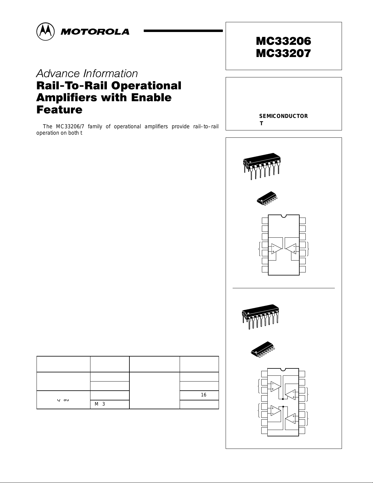
MC33206
P SUFFIX
PLASTIC PACKAGE
14
Output 1
Inputs 1
Enable 1
16
1
14
1
N.C.
1
2
N.C.
3
4
1
7
V
EE
(Dual, Top View)
MC33207
1
CASE 646
D SUFFIX
PLASTIC PACKAGE
CASE 751A
(SO–14)
N.C.
14
V
13
CC
Output 2
12
11
2
PLASTIC PACKAGE
Inputs 2
105
96
Enable 2
8
N.C.
P SUFFIX
CASE 648
ORDERING INFORMATION
Operational
Amplifier Function
This document contains information on a new product. Specifications and information herein
are subject to change without notice.
MOTOROLA ANALOG IC DEVICE DATA
Device
MC33206D
MC33206P
MC33207D
MC33207P Plastic DIP
Operating
Temperature Range
–
°
= –40 ° to +
A
°
Package
SO–14
Plastic DIP
SO–16
Motorola, Inc. 1996 Rev 0
16
1
Output 1
1
V
CC
Output 2
2
3
4
8
Inputs 1
Inputs 2 2
Enable 2, 3
1
(Quad, Top View)
D SUFFIX
PLASTIC PACKAGE
CASE 751B
(SO–16)
Enable 1, 4
16
Output 4
15
14
4
3
13
125
116
107
9
Inputs 4
V
EE
Inputs 3
Output 3
1
Page 2
MC33206 MC33207
MAXIMUM RATINGS
Rating Symbol Value Unit
Supply Voltage (VCC to VEE) V
ESD Protection Voltage at any Pin
Human Body Model
Voltage at any Device Pin V
Input Differential Voltage Range V
Common Mode Input Voltage Range (Note 2) V
Output Short Circuit Duration (Note 3) t
Maximum Junction Temperature T
Storage Temperature Range T
Maximum Power Dissipation P
NOTES: 1. The differential input voltage of each amplifier is limited by two internal parallel back–to–back
diodes. For additional differential input voltage range, use current limiting resistors in series
with the input pins.
2.The common–mode input voltage range of each amplifier is limited by diodes connected from
the inputs to both power supply rails. Therefore, the voltage on either input must not exceed
either supply rail by more than 500 mV.
3.Power dissipation must be considered to ensure maximum junction temperature (TJ) is not
exceeded.
4.ESD data available upon request.
V
S
ESD
DP
IDR
CM
s
J
stg
D
13 V
2,000 V
VS ± 0.5 V
(Note 1) V
VCC + 0.5 to
VEE – 0.5
(Note 3) sec
+150 °C
–65 to +150 °C
(Note 3) mW
V
DC ELECTRICAL CHARACTERISTICS (V
= 5.0 V, VEE = 0 V, V
CC
= 5.0 V, TA = 25°C, unless otherwise noted.)
Enable
Characteristic Figure Symbol Min Typ Max Unit
Input Offset Voltage (VCM 0 to 0.5 V, VCM 1.0 to 5.0 V)
MC33206: TA = 25°C
MC33201: TA = –40° to +105°C
MC33207: TA = 25°C
MC33202: TA = –40° to +105°C
Input Offset Voltage Temperature Coefficient (RS = 50 Ω)
– V
IO
–
–
–
–
0.5
1.0
0.5
1.0
8.0
11
10
13
– ∆VIO/∆T – 2.0 – µV/°C
TA = –40° to +105°C
Input Bias Current (VCM = 0 to 0.5 V, VCM = 1.0 to 5.0 V)
TA = 25°C
–
TA = –40° to +105°C
Input Offset Current (VCM = 0 to 0.5 V, VCM = 1.0 to 5.0 V)
– IIO
TA = 25°C
TA = –40° to +105°C
Common Mode Input Voltage Range – V
Large Signal Voltage Gain (VCC = 5.0 V, VEE = –5.0 V)
– A
RL = 10 kΩ
RL = 600 Ω
Output Voltage Swing (VID = ±0.2 V)
–
RL = 10 kΩ
RL = 10 kΩ
RL = 600 Ω
RL = 600 Ω
IIB
ICR
VOL
V
OH
V
OL
V
OH
V
OL
–
–
–
–
–
V
EE
50
25
4.85
–
4.75
–
80
100
5.0
10
VCC + 0.2
VEE – 0.2
300
250
4.95
0.05
4.85
0.15
200
250
50
100
V
CC
–
–
–
–
0.15
–
0.25
Common Mode Rejection (Vin = 0 to 5.0 V) – CMR 60 90 – dB
Power Supply Rejection Ratio
VCC/VEE = 5.0 V/Gnd to 3.0 V/Gnd
Output Short Circuit Current (Source and Sink) – I
– PSRR
PSR
SC
–
66
25
92
500
–
50 80 – mA
mV
nA
nA
V
kV/V
V
µV/V
dB
2
MOTOROLA ANALOG IC DEVICE DATA
Page 3
MC33206 MC33207
DC ELECTRICAL CHARACTERISTICS (continued) (V
Characteristic UnitMaxTypMinSymbolFigure
Power Supply Current (VO = 2.5 V, TA = –40° to +105°C,
per Amplifier)
MC33206: V
MC33206: V
MC33207: V
MC33207: V
Enable Input Voltage (per Amplifier)
Enabled – Amplifier “On”
Disabled – Amplifier “Off” (Standby)
Enable Input Current (Note 5) (per Amplifier)
V
V
V
V
NOTE: 5.External control circuitry must provide for an initial turn–off transient of <10 µA.
Enable
Enable
Enable
Enable
= 12 V
= 5.0 V
= 1.8 V
= Gnd
AC ELECTRICAL CHARACTERISTICS (V
Slew Rate (VS = ±2.5 V , VO = –2.0 to +2.0 V,
RL = 2.0 kΩ, AV = 1.0)
Gain Bandwidth Product (f = 100 kHz) – GBW – 2.2 – MHz
Phase Margin (RL = 600 Ω, CL = 0 pF) –
Gain Margin (RL = 600 Ω, CL = 0 pF) – A
Channel Separation (f = 1.0 Hz to 20 kHz, AV = 100) – CS – 90 – dB
Power Bandwidth (VO = 4.0 Vpp, RL = 600 Ω, THD ≤ 1%) – BW
Total Harmonic Distortion (RL = 600 Ω, VO = 1.0 Vpp, AV = 1.0)
f = 1.0 kHz
f = 10 kHz
Open Loop Output Impedance
(VO = 0 V, f = 2.0 MHz, AV = 10)
Differential Input Resistance (VCM = 0 V) – R
Differential Input Capacitance (VCM = 0 V) – C
Equivalent Input Noise Voltage (RS = 100 Ω)
f = 10 Hz
f = 1.0 kHz
Equivalent Input Noise Current
f = 10 Hz
f = 1.0 kHz
Time Delay for Device to Turn On – t
Time Delay for Device to Turn Off – t
= 5.0 Vdc
Enable
= Gnd (Standby)
Enable
= 5.0 Vdc
Enable
= Gnd (Standby)
Enable
= 5.0 V, VEE = 0 V, V
CC
Characteristic Figure Symbol Min Typ Max Unit
= 5.0 V, VEE = 0 V, V
CC
– I
– V
– I
Enable
– SR 0.5 1.0 – V/µs
–
– ZO – 100 – Ω
– e
– i
= 5.0 V, TA = 25°C, unless otherwise noted.)
Enable
D
–
–
–
–
Enable
Enable
= 5.0 V, TA = 25°C, unless otherwise noted.)
O
M
M
P
THD
in
in
n
n
on
off
–
–
–
–
–
–
– 65 – Deg
– 12 – dB
– 28 – kHz
–
–
– 200 – kΩ
– 8.0 – pF
–
–
–
–
– 10 – µs
– 2.0 – µs
0.8
0.5
1.5
0.5
VEE + 1.8
VEE + 0.3
2.5
2.2
0.8
0
0.002
0.008
25
20
0.8
0.2
1.125
6.0
2.25
6.0
–
–
–
–
–
–
–
–
–
–
pA/
–
–
mA
µA
mA
µA
V
µA
%
nV/
Hz
Hz
MOTOROLA ANALOG IC DEVICE DATA
3
Page 4
V
CC
Enable
MC33206 MC33207
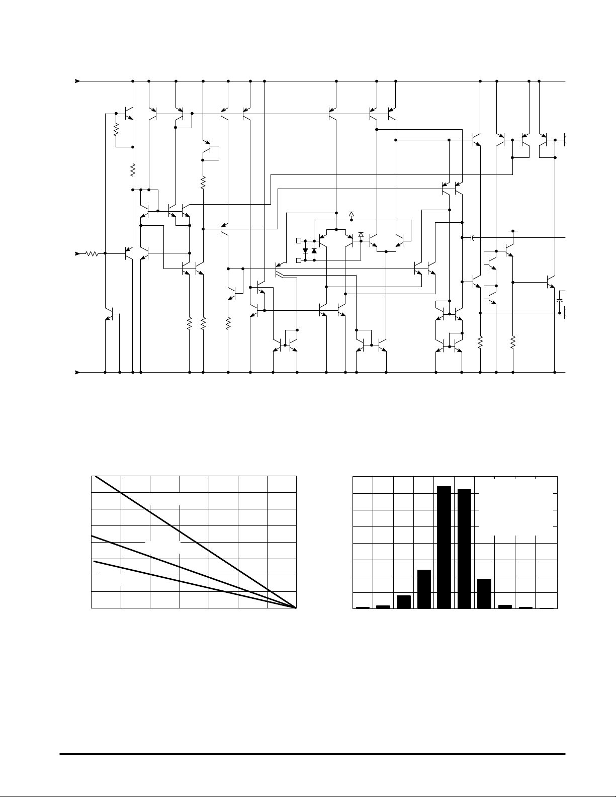
Figure 1. Circuit Schematic
(Each Amplifier)
V
CC
Vin –
Vin +
V
CC
V
CC
V
EE
4000
3500
3000
2500
2000
1500
1000
, MAXIMUM POWER DISSIPATION (mW)
500
0
D(max)
P
–60 –30
This device contains 96 active transistors (each amplifier).
Figure 2. Maximum Power Dissipation
versus T emperature
16 Pin DIP
14 Pin DIP
SO–14/SO–1
6
0 30 60 90 120 150
TA, AMBIENT TEMPERATURE (
°
C)
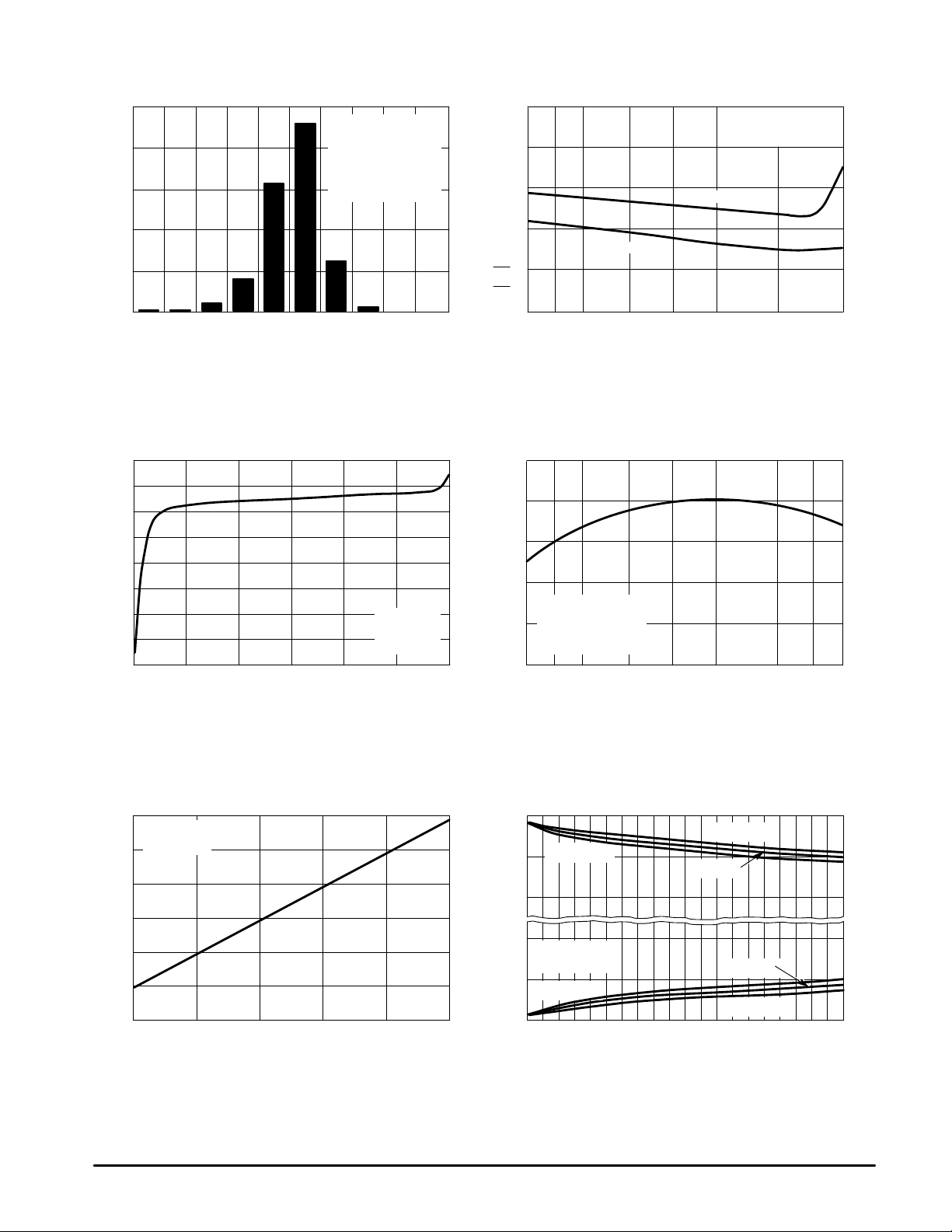
Figure 3. Input Offset Voltage Distribution
40
35
30
25
20
15
10
PERCENT AGE OF AMPLIFIERS (%)
5.0
0
–10 0 4.0 8.0 10–2.0 2.0 6.0–6.0–8.0 –4.0
360 amplifiers tested
from 3 wafer lots
VCC = 5.0 V
VEE = Gnd
TA = 25
DIP Package
VIO, INPUT OFFSET VOLTAGE (mV)
°
C
4
MOTOROLA ANALOG IC DEVICE DATA
Page 5
MC33206 MC33207
–
–
+
+
Figure 4. Input Offset Voltage
T emperature Coefficient Distribution
50
360 amplifiers tested
40
30
20
10
PERCENT AGE OF AMPLIFIERS (%)
0
–50 0 20 40 50–10 10 30–30–40 –20
TC
, INPUT OFFSET VOLTAGE TEMPERATURE COEFFICIENT (µV/°C)
V
IO
from 3 wafer lots
VCC = 5.0 V
VEE = Gnd
TA = 25
DIP Package
°
C
200
160
120
80
, INPUT BIAS CURRENT (nA)
40
IB
I
0
–55 –40 –25 0 25 70 85 125
Figure 6. Input Bias Current
versus Common Mode V oltage
150
100
50
0
–50
–100
–150
, INPUT BIAS CURRENT (nA)
IB
I
–200
–250
0 6.0 8.0 10 12 105
2.0 4.0
VCM, INPUT COMMON MODE VOLTAGE (V)
VCC = 12 V
VEE = Gnd
°
C
TA = 25
300
260
220
180
VCC = 5.0 V
VEE = Gnd
140
, OPEN LOOP VOL TAGE GAIN (kV/V)
A
RL = 600
∆
VOL
100
–55 –40 –25 0 25 70 85 125
Figure 5. Input Bias Current
versus T emperature
VCM = 0 V to 0.5 V
VCM > 1.0 V
TA, AMBIENT TEMPERATURE (
Figure 7. Open Loop Voltage Gain
versus T emperature
Ω
VO = 0.5 V to 4.5 V
TA, AMBIENT TEMPERATURE (
VCC = 5.0 V
VEE = Gnd
°
°
C)
C)
Figure 8. Output Voltage Swing
versus Supply V oltage
12
RL = 600
Ω
TA = 25°C
10
8.0
6.0
4.0
,OUTPUT VOLTAGE (Vpp)
2.0
O
V
0
±
1.0
±
2.0 105.0
VCC,
±
3.0
VEE
SUPPLY VOLTAGE (V)
±
4.0
MOTOROLA ANALOG IC DEVICE DATA
Figure 9. Output Saturation Voltage
versus Load Current
V
TA = –55°C
TA = 125°C
TA = 25°C
VCC = 5.0 V
VEE = –5.0 V
, OUTPUT SA TURATION VOLTAGE (V)
TA = 125°C
SAT
V
±
5.0
±
6.0
01520
IL, LOAD CURRENT (mA)
TA = 25°C
TA = –55°C
CC
VCC
VCC
VEE
VEE
V
EE
5
Page 6

MC33206 MC33207
12
9.0
6.0
VCC = 6.0 V
VEE = –6.0 V
, OUTPUT VOLTAGE (Vpp)
3.0
O
V
0
1.0 k 100 k 1.0 M10 k
RL = 600
AV = 1.0
°
TA = 25
Ω
C
Figure 12. Power Supply Rejection
120
100
80
60
40
VCC = 6.0 V
20
VEE = –6.0 V
°
to +125°C
TA = –55
PSR, POWER SUPPLY REJECTION (dB)
0
10
100 1.0 k 10 k 100 k 1.0 M
Figure 10. Output Voltage
versus Frequency
f, FREQUENCY (Hz)
versus Frequency
PSR+
PSR–
f, FREQUENCY (Hz)
Figure 11. Common Mode Rejection
versus Frequency
100
80
60
40
VCC = 6.0 V
VEE = –6.0 V
20
CMR, COMMON MODE REJECTION (dB)
0
10
°
to +125°C
TA = –55
100 1.0 k 10 k 100 k 1.0 M
f, FREQUENCY (Hz)
Figure 13. Output Short Circuit Current
versus Output Voltage
100
Source
80
60
40
20
, OUTPUT SHORT CIRCUIT CURRENT (mA)
SC
0
I
0 1.0 2.0 3.0 4.0 5.0 6.0
Sink
V
, OUTPUT VOLTAGE (V)
out
VCC = 6.0 V
VEE = –6.0 V
TA = 25
°
C
150
125
100
75
50
25
, OUTPUT SHORT CIRCUIT CURRENT (mA)
SC
I
6
Figure 14. Output Short Circuit Current
versus T emperature
VCC = 5.0 V
VEE = Gnd
Source
Sink
0
TA, AMBIENT TEMPERATURE (°C)
2.0
1.6
1.2
0.8
0.4
, SUPPLY CURRENT PER AMPLIFIER (mA)
CC
I
Figure 15. Supply Current per Amplifier
versus Supply V oltage with No Load
TA = 125°C
TA = 25°C
TA = –55°C
0
±
±
1.0
±
0
2.0
VCC, VEE
±
3.0
±
, SUPPLY VOLTAGE (V)
MOTOROLA ANALOG IC DEVICE DATA
4.0
±
5.0
±
.0–55 –40 –25 25 70 1250 85 105
Page 7

MC33206 MC33207
Figure 16. Slew Rate
versus T emperature
2.0
VCC = 2.5 V
VEE = –2.5 V
±
2.0 V
VO =
1.5
µ
1.0
SR, SLEW RA TE (V/ s)
0.5
0
–55 –40 –25 25 70 1250 85 105 –55 –40 –25 25 70 1250 85 105
TA, AMBIENT TEMPERATURE (°C)
+Slew Rate
–Slew Rate
4.0
3.0
2.0
1.0
GBW, GAIN BANDWIDTH PRODUCT (MHz)
0
Figure 18. V oltage Gain and Phase
versus Frequency
70
50
VS = ±6.0 V
°
C
TA = 25
Ω
RL = 600
40
80
70
50
Figure 17. Gain Bandwidth Product
versus T emperature
VCC = 2.5 V
VEE = –2.5 V
f = 100 kHz
TA, AMBIENT TEMPERATURE (
Figure 19. V oltage Gain and Phase
versus Frequency
°
C)
CL = 0 pF
TA = 25
RL = 600
40
°
C
Ω
80
30
10
1A – Phase, CL = 0 pF
1B – Gain, CL = 0 pF
–10
2A – Phase, CL = 300 pF
2B – Gain, CL = 300 pF
VOL
A , OPEN LOOP VOLTAGE GAIN (dB)
–30
10 k 100 k 1.0 M 10 M
f, FREQUENCY (Hz)
2A
2B
1B
Figure 20. Gain and Phase Margin
versus T emperature
70
60
50
VCC = 6.0 V
40
VEE = –6.0 V
Ω
RL = 600
30
CL = 100 pF
20
, PHASE MARGIN (DEGREES)
M
10
O
0
TA, AMBIENT TEMPERATURE (
Phase Margin
Gain Margin
°
C)
1A
120
160
200
240
30
10
1A – Phase, VS = ±6.0 V
1B – Gain, VS =
–10
, EXCESS PHASE (DEGREES)
O
2A – Phase, VS =
VOL
2B – Gain, VS =
A , OPEN LOOP VOLTAGE GAIN (dB)
–30
10 k 100 k 1.0 M 10 M
versus Differential Source Resistance
70
60
50
40
30
, GAIN MARGIN (dB)
20
A
10
0
75
60
VCC = 6.0 V
45
VEE = –6.0 V
TA = 25
30
M
15
, PHASE MARGIN (DEGREES)
M
O
0
2A
1B
±
6.0 V
±
1.0 V
±
1.0 V
f, FREQUENCY (Hz)
2B
Figure 21. Gain and Phase Margin
Phase Margin
°
C
Gain Margin
100 1.0 k 10 k 100 k–55 –40 –25 25 70 1250 85 105 10
RT, DIFFERENTIAL SOURCE RESISTANCE (Ω)
1A
120
160
200
240
75
60
45
30
15
0
MOTOROLA ANALOG IC DEVICE DATA
7
Page 8

MC33206 MC33207
Figure 22. Gain and Phase Margin
versus Capacitive Load
80
70
Phase Margin
60
Gain Margin
50
40
30
20
, PHASE MARGIN (DEGREES)
M
10
O
0
10 100 1.0 k
CL, CAPACITIVE LOAD (pF)
VCC = 6.0 V
VEE = –6.0 V
Ω
RL = 600
AV = 100
°
C
TA = 25
Figure 24. Channel Separation
versus Frequency
150
120
90
60
VCC = 6.0 V
VEE = –6.0 V
30
VO = 8.0 Vpp
CS, CHANNEL SEPARATION (dB)
0
100 1.0 k 10 k
TA = 25
°
C
f, FREQUENCY (Hz)
AV = 100
AV = 10
16
14
12
10
8.0
6.0
4.0
2.0
0
5.0
4.0
3.0
2.0
, GAIN MARGIN (dB)
, OUTPUT VOL TAGE (Vpp)
M
A
O
1.0
V
0
10
1.0
0.1
0.01
THD, TOT AL HARMONIC DISTORTION (%)
0.001
Figure 23. Output Voltage
versus Load Resistance
VCC = 5.0 Vdc
VEE = Gnd
CL = 0 pF
AV = 1.0
°
C
TA = 25
100 1.0 k 10 k 100 k10
RL, LOAD RESISTANCE
VCC = 2.0 Vdc
Figure 25. T otal Harmonic Distortion
versus Frequency
VCC = 5.0 V
°
TA = 25
VO = 2.0 Vpp
AV = 1000
AV = 100
AV = 10
AV = 1.0
10 100 1.0 k 100 k
VEE = –5.0 V
C
RL = 600
f, FREQUENCY (Hz)
Ω
10 k
Figure 26. Equivalent Input Noise V oltage
and Current versus Frequency
50
40
30
20
10
0
n
10
e , EQUIVALENT INPUT NOISE VOLTAGE (nV/ Hz)
Noise Voltage
Noise Current
100 10 k 100 k
1.0 k
f, FREQUENCY (Hz)
VCC = 6.0 V
VEE = –6.0 V
TA = 25
8
5.0
4.0
°
C
3.0
2.0
1.0
0
n
i , INPUT REFERRED NOISE CURRENT (pA/ Hz)
MOTOROLA ANALOG IC DEVICE DATA
Page 9

MC33206 MC33207
GENERAL INFORMATION
The MC33206/7 family of operational amplifiers are
unique in their ability to swing rail–to–rail on both the input
and the output with a completely bipolar design. This offers
low noise, high output current capability and a wide common
mode input voltage range even with low supply voltages.
Operation is guaranteed over an extended temperature
range and at supply voltages of 2.0 V, 3.3 V and 5.0 V and
ground.
Since the common mode input voltage range extends from
VCC to VEE, it can be operated with either single or split
voltage supplies. The MC33206/7 are guaranteed not to latch
or phase reverse over the entire common mode range,
however, the inputs should not be allowed to exceed
maximum ratings.
CIRCUIT INFORMATION
Rail–to–rail performance is achieved at the input of the
amplifiers by using parallel NPN–PNP differential input
stages. When the inputs are within 800 mV of the negative
rail, the PNP stage is on. When the inputs are more than
800 mV greater than VEE, the NPN stage is on. This
switching of input pairs will cause a reversal of input bias
currents (see Figure 6). Also, slight differences in offset
voltage may be noted between the NPN and PNP pairs.
Cross–coupling techniques have been used to keep this
change to a minimum.
In addition to its rail–to–rail performance, the output stage
is current boosted to provide 80 mA of output current,
enabling the op amp to drive 600 Ω loads. Because of this
high output current capability, care should be taken not to
exceed the 150°C maximum junction temperature.
Enable Function
The MC33206/07 enable pins allow the user to externally
control the device. (Refer to the Pin Diagram on the first page
of this data sheet for enable pin connections.) If the enable
pins are pulled low (Gnd) each amplifier (MC33206) and
amplifier pair (MC33207) will be disabled. When the enable
pins are at a logic high (V
will turn “on”. Refer to the data sheet characteristics for the
required levels needed to change logical state.
The time to change states (from device “on” to “off” and
“off” to “on”) is defined as the time delay. The Circuit in
Figure 27 is used to measure ton and t
measurements are shown in Figures 28 and 29. When the
device is turned off (V
Enable
shut off disabling the amplifier.
Figure 27. Test Circuit for ton and t
MC33206
2.0 V
V
Enable
ton t
off
≥ VEE = 1.8 V) the amplifiers
Enable
. Typical ton and t
off
= Gnd) an internal regulator is
off
V
CC
2.0 k
V
out
ton t
off
off
Figure 28. ton Response
(2.0 V/DIV)
in
(1.0 V/DIV), V
O
V
ton, TIME (2.0 µs/DIV)
(2.0 V/DIV)
in
(1.0 V/DIV), V
O
V
Figure 29. t
t
, TIME (2.0 µs/DIV)
off
Response
off
Low V oltage Operation
The MC33206/07 will operate at supply voltages down to
1.8 V and ground. Since this device is a rail–to–rail on both
the input and output, one can be assured of continued
operation in battery applications when battery voltages drop
to low voltage levels. This is called End of Discharge (see
Figure 30). Now, the user can select a minimum quantity of
batteries best suited for the particular design depending on
the type of battery chosen. This will minimize part count in
many designs.
Figure 30. T ypical Battery Characteristics
Type Operating Voltage End of Discharge
Alkaline 1.5 V 0.9 V
NiCd 1.2 V 1.0 V
NiMh 1.2 V 1.0 V
Silver Oxide 1.6 V 1.3 V
Lithium Ion 3.6 V 2.5 V
Compensating for Output Capacitance
The combination of device output impedance and
increasing capacitive loading will cause phase delay
(reducing the phase margin) in any amplifier (Figure 22). If
the loading is excessive, the resulting response can be circuit
oscillation. In other words, an amplifier can become unstable
when the phase becomes greater than 180 degrees before
the open loop gain drops to unity gain. Figures 18 and 19
show this situation as frequency increases for a given load.
The MC33206/7 can typically drive up to 300 pF loads at
unity gain without oscillating.
MOTOROLA ANALOG IC DEVICE DATA
9
Page 10

MC33206 MC33207
Figure 31. Capacitive Loads Compensation
R
f
C
X
R
O
V
in
C
L
R
L
There are several ways to compensate for this
phenomena. Adding series resistance to the output is one
way, but not an ideal solution. A dc voltage error will occur at
the output. A better design solution to compensate for higher
capacitive loads would be to use the circuit in Figure 31. This
design helps to counteract the loss of phase margin by taking
the high frequency output signal and feeding it back into the
amplifier inverting input. This technique helps to overcome
oscillation due to a highly capacitive load. Keep in mind that
compensation will have the affect of lowering the Gain
Bandwidth Product (GPW). The values of CX and R0, are
determined experimentally. Typical CX and CL will be the
same value.
Figure 32. Noninverting Amplifier Slew Rate Figure 33. Small Signal Transient Response
VCC = 6.0 V
VEE = –6.0 V
Ω
RL = 600
CL = 100 pF
°
C
TA = 25
, OUTPUT VOLTAGE (2.0 mV/DIV)
O
V
SPICE Model
If a SPICE Macromodel is desired for the MC33206/07,
the user can define the characteristics from the following
information. Obtain the SPICE Macromodel for the MC33204
Rail–to–Rail Operational Amplifier (device is the same as the
MC33207). For the Enable feature of the MC33207, simulate
it as a bipolar switch. The Macromodel does not include an
input capacitance between the inverting and noninverting
inputs. This capacitor is called Cin. Add 3.0 to 5.0 pF if
stability analysis is required.
VCC = 6.0 V
VEE = –6.0 V
Ω
RL = 600
CL = 100 pF
°
C
TA = 25
, OUTPUT VOLTAGE (50 mV/DIV)V
O
10
t, TIME (5.0 µs/DIV)
, OUTPUT VOLTAGE (2.0 V/DIV)V
O
Figure 34. Large Signal Transient Response
VCC = 6.0 V
VEE = –6.0 V
Ω
RL = 600
CL = 100 pF
AV = 1.0
°
C
TA = 25
t, TIME (10 µs/DIV)
MOTOROLA ANALOG IC DEVICE DATA
t, TIME (10
µ
s/DIV)
Page 11

MC33206 MC33207
OUTLINE DIMENSIONS
14 8
B
17
A
F
C
N
HG D
–A–
14 8
G
–T–
SEATING
PLANE
D 14 PL
0.25 (0.010) A
SEATING
PLANE
71
M
–B–
T
K
P 7 PL
C
K
S
B
P SUFFIX
PLASTIC PACKAGE
CASE 646–06
ISSUE L
L
J
M
D SUFFIX
PLASTIC PACKAGE
CASE 751A–03
(SO–14)
ISSUE F
0.25 (0.010) B
M
X 45
R
_
M
S
NOTES:
1. LEADS WITHIN 0.13 (0.005) RADIUS OF TRUE
POSITION AT SEATING PLANE AT MAXIMUM
MATERIAL CONDITION.
2. DIMENSION L TO CENTER OF LEADS WHEN
FORMED PARALLEL.
3. DIMENSION B DOES NOT INCLUDE MOLD
FLASH.
4. ROUNDED CORNERS OPTIONAL.
DIM MIN MAX MIN MAX
A 0.715 0.770 18.16 19.56
B 0.240 0.260 6.10 6.60
C 0.145 0.185 3.69 4.69
D 0.015 0.021 0.38 0.53
F 0.040 0.070 1.02 1.78
G 0.100 BSC 2.54 BSC
H 0.052 0.095 1.32 2.41
J 0.008 0.015 0.20 0.38
K 0.115 0.135 2.92 3.43
L 0.300 BSC 7.62 BSC
M 0 10 0 10
____
N 0.015 0.039 0.39 1.01
NOTES:
1. DIMENSIONING AND TOLERANCING PER ANSI
Y14.5M, 1982.
2. CONTROLLING DIMENSION: MILLIMETER.
3. DIMENSIONS A AND B DO NOT INCLUDE
MOLD PROTRUSION.
4. MAXIMUM MOLD PROTRUSION 0.15 (0.006)
PER SIDE.
5. DIMENSION D DOES NOT INCLUDE DAMBAR
M
F
J
PROTRUSION. ALLOWABLE DAMBAR
PROTRUSION SHALL BE 0.127 (0.005) TOTAL
IN EXCESS OF THE D DIMENSION AT
MAXIMUM MATERIAL CONDITION.
DIM MIN MAX MIN MAX
A 8.55 8.75 0.337 0.344
B 3.80 4.00 0.150 0.157
C 1.35 1.75 0.054 0.068
D 0.35 0.49 0.014 0.019
F 0.40 1.25 0.016 0.049
G 1.27 BSC 0.050 BSC
J 0.19 0.25 0.008 0.009
K 0.10 0.25 0.004 0.009
M 0 7 0 7
P 5.80 6.20 0.228 0.244
R 0.25 0.50 0.010 0.019
MILLIMETERSINCHES
INCHESMILLIMETERS
____
–A–
916
B
18
F
S
H
G
D
16 PL
K
0.25 (0.010) T
MOTOROLA ANALOG IC DEVICE DATA
P SUFFIX
PLASTIC PACKAGE
CASE 648–08
ISSUE R
C
SEATING
–T–
PLANE
J
M
M
A
L
M
NOTES:
1. DIMENSIONING AND TOLERANCING PER ANSI
Y14.5M, 1982.
2. CONTROLLING DIMENSION: INCH.
3. DIMENSION L TO CENTER OF LEADS WHEN
FORMED PARALLEL.
4. DIMENSION B DOES NOT INCLUDE MOLD FLASH.
5. ROUNDED CORNERS OPTIONAL.
DIM MIN MAX MIN MAX
A 0.740 0.770 18.80 19.55
B 0.250 0.270 6.35 6.85
C 0.145 0.175 3.69 4.44
D 0.015 0.021 0.39 0.53
F 0.040 0.70 1.02 1.77
G 0.100 BSC 2.54 BSC
H 0.050 BSC 1.27 BSC
J 0.008 0.015 0.21 0.38
K 0.110 0.130 2.80 3.30
L 0.295 0.305 7.50 7.74
M 0 10 0 10
S 0.020 0.040 0.51 1.01
MILLIMETERSINCHES
____
11
Page 12

–T–
MC33206 MC33207
OUTLINE DIMENSIONS
D SUFFIX
PLASTIC PACKAGE
CASE 751B–05
(SO–16)
–A–
16 9
–B–
18
8 PLP
G
K
C
SEATING
PLANE
D
16 PL
0.25 (0.010) A
M
S
B
T
S
ISSUE J
0.25 (0.010) B
M
NOTES:
1. DIMENSIONING AND TOLERANCING PER ANSI
Y14.5M, 1982.
2. CONTROLLING DIMENSION: MILLIMETER.
3. DIMENSIONS A AND B DO NOT INCLUDE
MOLD PROTRUSION.
4. MAXIMUM MOLD PROTRUSION 0.15 (0.006)
M
S
R
X 45
_
F
J
PER SIDE.
5. DIMENSION D DOES NOT INCLUDE DAMBAR
PROTRUSION. ALLOWABLE DAMBAR
PROTRUSION SHALL BE 0.127 (0.005) TOTAL
IN EXCESS OF THE D DIMENSION AT
MAXIMUM MATERIAL CONDITION.
DIM MIN MAX MIN MAX
A 9.80 10.00 0.386 0.393
B 3.80 4.00 0.150 0.157
C 1.35 1.75 0.054 0.068
D 0.35 0.49 0.014 0.019
F 0.40 1.25 0.016 0.049
G 1.27 BSC 0.050 BSC
J 0.19 0.25 0.008 0.009
K 0.10 0.25 0.004 0.009
M 0 7 0 7
____
P 5.80 6.20 0.229 0.244
R 0.25 0.50 0.010 0.019
INCHESMILLIMETERS
Motorola reserves the right to make changes without further notice to any products herein. Motorola makes no warranty , representation or guarantee regarding
the suitability of its products for any particular purpose, nor does Motorola assume any liability arising out of the application or use of any product or circuit, and
specifically disclaims any and all liability, including without limitation consequential or incidental damages. “T ypical” parameters which may be provided in Motorola
data sheets and/or specifications can and do vary in different applications and actual performance may vary over time. All operating parameters, including “Typicals”
must be validated for each customer application by customer’s technical experts. Motorola does not convey any license under its patent rights nor the rights of
others. Motorola products are not designed, intended, or authorized for use as components in systems intended for surgical implant into the body, or other
applications intended to support or sustain life, or for any other application in which the failure of the Motorola product could create a situation where personal injury
or death may occur. Should Buyer purchase or use Motorola products for any such unintended or unauthorized application, Buyer shall indemnify and hold Motorola
and its officers, employees, subsidiaries, affiliates, and distributors harmless against all claims, costs, damages, and expenses, and reasonable attorney fees
arising out of, directly or indirectly, any claim of personal injury or death associated with such unintended or unauthorized use, even if such claim alleges that
Motorola was negligent regarding the design or manufacture of the part. Motorola and are registered trademarks of Motorola, Inc. Motorola, Inc. is an Equal
Opportunity/Affirmative Action Employer.
How to reach us:
USA/EUROPE/Locations Not Listed: Motorola Literature Distribution; JAP AN: Nippon Motorola Ltd.; Tatsumi–SPD–JLDC, 6F Seibu–Butsuryu–Center,
P.O. Box 20912; Phoenix, Arizona 85036. 1–800–441–2447 or 602–303–5454 3–14–2 Tatsumi Koto–Ku, Tokyo 135, Japan. 03–81–3521–8315
MFAX: RMF AX0@email.sps.mot.com – TOUCHT ONE 602–244–6609 ASIA/PACIFIC: Motorola Semiconductors H.K. Ltd.; 8B Tai Ping Industrial Park,
INTERNET: http://Design–NET.com 51 Ting Kok Road, Tai Po, N.T ., Hong Kong. 852–26629298
12
◊
MOTOROLA ANALOG IC DEVICE DATA
MC33206/D
*MC33206/D*
 Loading...