

Page 1
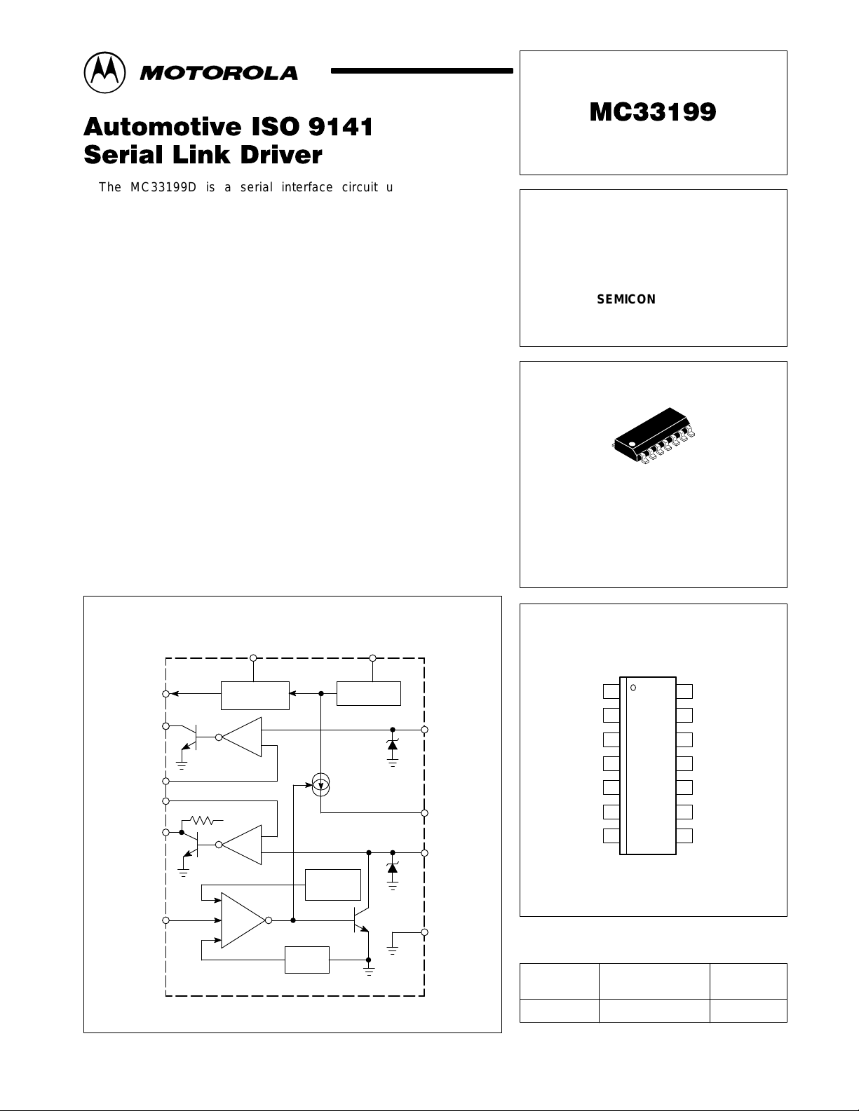
The MC33199D is a serial interface circuit used in diagnostic
applications. It is the interface between the microcontroller and the special
K and L Lines of the ISO diagnostic port. The MC33199D has been
designed to meet the “Diagnosis System ISO 9141” specification.
The device has a bi–directional bus K Line driver, fully protected against
short circuits and over temperature. It also includes the L Line receiver,
used during the wake up sequence in the ISO transmission.
The MC33199 has a unique feature which allows transmission baud rate
up to 200 k baud.
• Electrically Compatible with Specification “Diagnosis System ISO 9141”
• Transmission Speed Up to 200 k Baud
• Internal Voltage Reference Generator for Line Comparator Thresholds
• TXD, RXD and LO Pins are 5.0 V CMOS Compatible
• High Current Capability of DIA Pin (K Line)
• Short Circuit Protection for the K Line Input
• Over Temperature Shutdown with Hysteresis
• Large Operating Range of Driver Supply Voltage
• Full Operating Temperature Range
• ESD Protected Pins
Order this document by MC33199/D
ISO 9141
SERIAL LINK DRIVER
SEMICONDUCTOR
TECHNICAL DATA
14
1
D SUFFIX
PLASTIC PACKAGE
CASE 751A
(SO–14)
REF–OUT
LO
REF–IN–L
REF–IN–K
RXD
TXD
Simplified Application
V
CC
Reference
Generator
+
C2
–
V
CC
–
C1
+
Thermal
Shutdown
Driver
Current
Limit
This device contains 94 active transistors.
Protection
I1
Source
V
S
L
I1
DIA
Gnd
PIN CONNECTIONS
V
CC
REF–IN–L
REF–IN–K
LO
RXD
TXD
NC
114
2
3
4
5
6
7
(Top View)
REF–OUT
V
13
L
12
I1
11
Gnd
10
DIA
9
NC
8
S
ORDERING INFORMATION
Operating
Device
MC33199D TA = – 40° to +125°C SO–14
Temperature Range
Package
MOTOROLA ANALOG IC DEVICE DATA
Motorola, Inc. 1996 Rev 0
1
Page 2
MC33199
MAXIMUM RATINGS
(Note 1)
Rating
Symbol Value Unit
VS Supply Pin
DC Voltage Range
Transient Pulse (Note 2)
VCC Supply DC Voltage Range V
DIA and L Pins (Note 2)
DC Voltage Range
Transient Pulse (Clamped by Internal Diode)
DC Source Current
DIA Low Level Sink Current
V
pulse
V
S
CC
–
–0.5 to +40
–2.0 to +40
–0.3 to +6.0 V
–0.5 to +40
–2.0
–50
Int. Limit
TXD DC Voltage Range – –0.3 to
V
CC
REF–IN DC Voltage Range
VS < V
CC
VS > V
CC
ESD Voltage Capability (Note 3) V
NOTES: 1. The device is compatible with Specification: “Diagnosis System ISO 9141”.
2.See the test circuit (Figure 23). Transient test pulse according to ISO 76371 and DIN 40839;
highest test levels.
3.Human Body Model; C = 100 pF, R = 1500 Ω.
–
(ESD)
–0.3 to V
–0.3 to V
±2000 V
THERMAL RATINGS
Rating Symbol Value Unit
Storage Temperature T
Operating Junction Temperature T
Thermal Resistance, Junction–to–Ambient R
Maximum Power Dissipation (@ TA = 105°C) P
stg
J
θJA
D
–55 to +150 °C
–40 to +150 °C
V
V
V
mA
mA
V
+ 0.3
V
CC
S
180 °C/W
250 mW
ELECTRICAL CHARACTERISTICS (– 40°C ≤ T
≤ 125°C, 4.5 V ≤ VCC ≤ 5.5 V, 4.5 V ≤ VS ≤ 20 V, unless otherwise
A
noted. Typical values reflect approximate mean at 25°C, nominal VCC and VS, at time of device characterization.)
Characteristic
Symbol Min Typ Max Unit
VCC PIN 1
VCC Supply Voltage Range V
VCC Supply Current (Note 1) I
CC
CC
4.5 – 5.5 V
0.5 1.0 1.5 mA
REF–IN–L PIN 2 AND REF–IN–K PIN 3
REF–IN–L and REF–IN–K Input Voltage Range
For 0 < VS < V
For VCC < VS < 40 V
CC
REF–IN–L and REF–IN–K Inputs Currents I
V
inref
VIN
2.0
2.0
–
–
VCC – 2.0 V
VS – 1.0 V
–5.0 – 5.0 µA
LO PIN 4
LO Open Collector Output
Low Level Voltage @ I
Low Level Voltage @ I
out
out
= 1.0 mA
= 4.0 mA
V
OL
–
–
0.34
–
0.7
0.8
RXD PIN 5
Pull–Up Resistor to V
Low Level Voltage @ I
NOTES: 1. Measured with TXD = VCC, I1 = VS, DIA and L high, no load. REF–IN–L and REF–IN–K connected to REF–OUT .
2.0 < VCC < 5.5 V, 0 < VS < 40 V, 0 < V
3.When an over temperature is detected, the DIA output is forced “off”.
4.0 < VCC < 5.5 V, 0 < VS < 40 V, 0 < VL < 20 V.
5.At static “High” or “Low” level TXD, the current source I1 delivers a current of 3.0 mA (typ). Only during “Low” to “High” transition, does this current
increase to a higher value in order to charge the K Line capacitor (CL < 4.0 nF) in a short time (see Figure 3).
6.Measured with TXD = VCC, I1 = VS, DIA and L high, no load, REF–IN–L and REF–IN–K connected to REF–OUT .
CC
= 1.0 mA V
out
< 20 V, TXD high or floating.
DIA
R
RXD
OL
1.5 2.0 2.5 kΩ
– 0.3 0.7 V
V
V
2
MOTOROLA ANALOG IC DEVICE DATA
Page 3
MC33199
ELECTRICAL CHARACTERISTICS (continued) (– 40°C ≤ T
≤ 125°C, 4.5 V ≤ VCC ≤ 5.5 V, 4.5 V ≤ VS ≤ 20 V, unless otherwise
A
noted. Typical values reflect approximate mean at 25°C, nominal VCC and VS, at time of device characterization.)
Characteristic UnitMaxTypMinSymbol
TXD PIN 6
High Level Input Voltage V
Low Level Input Voltage V
IH
IL
0.7 V
CC
2.8 – V
– 2.0 0.3 V
Input Current @ 0 < VS < 40 V
TXD at High Level
TXD at Low Level
I
H
I
L
–200
–600
–
–
30
–100
DIA INPUT/OUTPUT PIN 9
Low Level Output Voltage @ I = 30 mA V
Drive Current Limit I
High Level Input Threshold Voltage
(REF–IN–K Connected to REF–OUT)
Low Level Input Threshold Voltage
(REF–IN–K Connected to REF–OUT)
Input Hysteresis V
Positive Clamp @ 5.0 mA V
Negative Clamp @ – 5.0 mA V
Leakage Current (Note 2) I
Over T emperature Shutdown (Note 3) T
OL
Lim
V
IH
V
IL
Hyst
Cl+
Cl–
Leak
Lim
0 0.35 0.8 V
40 – 120 mA
V
min
ref
+ 0.25 V
V
min
ref
– 0.2 V
V
ref
+ 0.325 V
V
ref
– 0.125 V
V
ref
+ 0.4 V
V
ref
– 0.05 V
300 450 600 mV
37 40 44 V
–1.5 –0.6 –0.3 V
4.0 10 16 µA
155 – – °C
L INPUT PIN 12
High Level Input Threshold Voltage
(REF–IN–L Connected to REF–OUT)
Low Level Input Threshold Voltage
(REF–IN–L Connected to REF–OUT)
Input Hysteresis V
Leakage Current (Note 4) I
Positive Clamp @ 5.0 mA V
Negative Clamp @ – 5.0 mA V
V
IH
V
IL
Hyst
Leak
Cl+
Cl–
V
min
ref
+ 0.25 V
V
min
ref
– 0.2 V
V
ref
+ 0.325 V
V
ref
– 0.125 V
V
ref
+ 0.4 V
V
ref
– 0.05 V
300 450 600 mV
4.0 10 16 µA
37 40 44 V
–1.5 –0.6 –0.3 V
I1 PIN 11
Static Source Current I1
Static Saturation Voltage (I1s = – 2.0 mA) V
I1(sat)
Dynamic Source Current (Note 5) I1
Dynamic Saturation Voltage (I
= – 40 mA) V
I1(sat)
I1(dsat)
s
d
–4.0 –3.0 –2.0 mA
VS – 1.2 VS – 0.8 V
–120 –80 –40 mA
VS – 2.7 VS – 0.85 V
VS PIN 13
VS Supply Voltage Range V
VS Supply Current (Note 6) I
NOTES: 1. Measured with TXD = VCC, I1 = VS, DIA and L high, no load. REF–IN–L and REF–IN–K connected to REF–OUT .
2.0 < VCC < 5.5 V, 0 < VS < 40 V, 0 < V
3.When an over temperature is detected, the DIA output is forced “off”.
4.0 < VCC < 5.5 V, 0 < VS < 40 V, 0 < VL < 20 V.
5.At static “High” or “Low” level TXD, the current source I1 delivers a current of 3.0 mA (typ). Only during “Low” to “High” transition, does this current
increase to a higher value in order to charge the K Line capacitor (CL < 4.0 nF) in a short time (see Figure 3).
6.Measured with TXD = VCC, I1 = VS, DIA and L high, no load, REF–IN–L and REF–IN–K connected to REF–OUT .
< 20 V, TXD high or floating.
DIA
S
S
4.5 – 20 V
0.5 1.3 2.0 mA
CC
max
max
max
max
S
S
V
µA
V
V
V
V
V
V
MOTOROLA ANALOG IC DEVICE DATA
3
Page 4
MC33199
ELECTRICAL CHARACTERISTICS (continued)
(– 40°C ≤ TA ≤ 125°C, 4.5 V ≤ VCC ≤ 5.5 V, 4.5 V ≤ VS ≤ 20 V, unless otherwise
noted. Typical values reflect approximate mean at 25°C, nominal VCC and VS, at time of device characterization.)
Characteristic UnitMaxTypMinSymbol
REF–OUT PIN 14
Output Voltage
3.0 < VS < 5.6 V and IRO = ±10 µA
5.6 < VS < 18 V and IRO = ±10 µA
18 < VS < 40 V and IRO = ±10 µA
Maximum Output Current I
Pull–Up Resistor to V
NOTES: 1. Measured with TXD = VCC, I1 = VS, DIA and L high, no load. REF–IN–L and REF–IN–K connected to REF–OUT .
2.0 < VCC < 5.5 V, 0 < VS < 40 V, 0 < V
3.When an over temperature is detected, the DIA output is forced “off”.
4.0 < VCC < 5.5 V, 0 < VS < 40 V, 0 < VL < 20 V.
5.At static “High” or “Low” level TXD, the current source I1 delivers a current of 3.0 mA (typ). Only during “Low” to “High” transition, does this current
increase to a higher value in order to charge the K Line capacitor (CL < 4.0 nF) in a short time (see Figure 3).
6.Measured with TXD = VCC, I1 = VS, DIA and L high, no load, REF–IN–L and REF–IN–K connected to REF–OUT .
DYNAMIC CHARACTERISTICS (– 40°C ≤ T
CC
< 20 V, TXD high or floating.
DIA
≤ 125°C, 4.5 V ≤ VCC ≤ 5.5 V, 4.5 V ≤ VS ≤ 20 V, unless otherwise noted.)
A
V
ref
out
R
PU
2.7
0.5 x V
8.5
S
–
–
–
3.3
0.56 x V
10.8
S
–50 – 50 µA
3.0 8.0 12 kΩ
Characteristic Symbol Min Typ Max Unit
Transmission Speed 1/t Bit 0 – 200 k Baud
High or Low Bit Time t Bit 5.0 – – µs
RXD Output
Low to High Transition Delay Time
High to Low Transition Delay Time
t
RDR
t
RDF
–
–
–
–
450
450
LO Output
Low to High Transition Delay Time
High to Low Transition Delay Time
t
LDR
t
LDF
–
–
–
–
2.0
2.0
DIA Output
Low to High Transition Delay Time
High to Low Transition Delay Time
t
DDR
t
DDF
–
–
–
–
650
650
I1 Output (VS – I1 > 2.7 V)
Rise Time
Hold Time
t
I1R
t
I1F
1.5
–
–
–
0.3
4.5
V
ns
µs
ns
µs
4
MOTOROLA ANALOG IC DEVICE DATA
Page 5

MC33199
Figure 1. TXD to DIA AC Characteristic
Test
Points
Input
Signal
2.0 K
2 x 30 pF
+ 5.0 V
+12 V
V
CCVbat
REF–OUT
REF–IN–L
REF–IN–K
TXD
I1
Test
Point
DIA
1.0 nF
Gnd
5.0 V
0 V
DIA Output
Signal
t
DDR
10 V
Figure 2. DIA to TXD and L to LO AC Characteristics
+ 5.0 V +12 V
V
CCVbat
REF–OUT
REF–IN–L
REF–IN–K
TXD
LO
RXD
DIA
Gnd
L
Input
Signal
12 V
0 V
RXD to LO
Output Signal
t
Bit
t
RDR/tLDR
4.5 V
TXD Input
Signal
t
DDF
2.0 V
t
Bit
DIA and L
Input Signal
t
RDF/tLDF
0.4 V
Figure 3. Current Source I1 AC Characteristics
t
Bit
TXD
Signal
t
I1H
120 mA
40 mA
4.0 mA
2.0 mA
At static “High” or “Low” level TXD, the current source I1 delivers a
current of 3.0 mA (typ). Only during “Low” to “High” transition, does this
current increase to a higher value in order to charge the K Line
capacitor (Cl < 4.0 nF) in a short time.
t
I1R
t
I1F
Typical I1
Waveform
Current Source
I1 Minimum Limit
5.0 V
0 V
Current Source
I1 Maximum Limit
MOTOROLA ANALOG IC DEVICE DATA
Figure 4. Current Source I1 and DIA Discharge
Current Test Schematic
I1 Pulse
Current
I1
DIA Discharge
Current
33 nF
To
Oscilloscope
Ω
10
Input
Signal
+ 5.0 V +12 V
V
CCVbat
REF–OUT
REF–IN–L
REF–IN–K
TXD
LO
RXD
DIA
Gnd
5
Page 6

MC33199
Figure 5. Logic Diagram and Application Schematic
V
bat
MCU
REF–OUT
LO
REF–IN–L
REF–IN–K
RXD
TXD
VCC = 5.0 V
Reference
Generator
+
C2
–
V
CC
–
C1
+
Driver
Current
Limit
Car Electronic Control Unit
V
Protection
I1
Source
Thermal
Shutdown
S
L
I1
DIA
Gnd
L Line
K Line
R
PU
Service Tester or
End of Line
Manufacturer
Programmation or
Checking System
TXD
RXD
Figure 6. T ypical Application with Several ECUs
+V
bat
MC33199MCU
ECU #1
Car ISO Diagnostic
Connector
MC33199MCU
ECU #2
Car
R
PU
L Line
K Line
Service Tester or
End of Line
Manufacturer
Programmation or
Checking System
Other
ECUs
6
MOTOROLA ANALOG IC DEVICE DATA
Page 7

MC33199
1.4
1.2
1.0
0.8
, SUPPLY CURRENT (mA)
CC
0.6
I
0.4
, SUPPLY CURRENT (mA)
S
I
5.0
–50
30
25
20
15
10
Figure 7. ICC Supply Current
versus T emperature
– 25 0 25 50 75 100 125
TA, AMBIENT TEMPERATURE (°C)
Figure 9. IS Supply Current
versus VS Supply Voltage
–40
°
C
25°C
125
°
C
2.5
2.0
1.5
1.0
, SUPPLY CURRENT (mA)
S
I
0.5
, VOLTAGE (V)
S
V
0
5.0
40
VCC = 5.5 V
V
DIA
35
30
25
20
Figure 8. IS Supply Current
versus VS Supply Voltage
25°C
10 15 20
VS, SUPPLY VOLTAGE (V)
Figure 10. VS Voltage
versus IS Current
= VL = VI1 = 20 V
125°C
–40°C
125
–40°C
°
C
25°C
REF–OUT, OUTPUT VOLTAGE (V)
10
8.0
6.0
4.0
2.0
0
5.0
10 15 20 25 30 35 40
VS, SUPPLY VOLTAGE (V)
Figure 11. REF–OUT Voltage
versus VS Supply Voltage
0
5.0 10 15 20 25 30 35 40
0
VS, VOLTAGE (V)
REF–OUT, OUTPUT VOLTAGE (V)
15
– 5.0
–1.0 3.0 7.0 1 1 15
IS, CURRENT (mA)
Figure 12. REF–OUT Voltage
versus REF–OUT Current
10
VS = 18 V
8.0
6.0
4.0
2.0
0
–40–30–20–100 1020304050
–50
REF–OUT, OUTPUT CURRENT (µA)
VS = 6.0 V
MOTOROLA ANALOG IC DEVICE DATA
7
Page 8

MC33199
Figure 13. L and DIA Hysteresis
versus Ambient T emperature
500
480
460
440
, L AND DIA HYSTERESIS (mV)
420
Hyst
V
400
– 25 0 25 50 75 100 125
–50
Figure 15. DIA Saturation Voltage
550
I
= 40 mA
DIA
500
TA, AMBIENT TEMPERATURE (°C)
versus T emperature
µ
, DIA AND L CURRENT ( A)
I
,
I
L
DIA
12
10
8.0
6.0
4.0
70
66
Figure 14. L and DIA Current
versus L and DIA Voltage
25°C
125
0
10 15 20
5.0 25 35 4030
V
, VL, DIA AND L VOLTAGE (V)
DIA
Figure 16. DIA Current Limit
versus T emperature
–40°C
°
C
450
400
, DIA SATURATION VOL TAGE (mV)
350
DIA(sat)
V
300
– 50 – 25 0 25 50 75 100 125
°
TA, AMBIENT TEMPERATURE (
C)
Figure 17. RXD Pull–Up Resistor
versus T emperature
2.5
Ω
2.4
2.3
2.2
2.1
2.0
1.9
1.8
, RXD PULL–UP RESISTOR (k )
1.7
RXD
1.6
R
1.5
– 50 – 25 0 25 50 75 100 125 – 50 – 25 0 25 50 75 100 125
TA, AMBIENT TEMPERATURE (°C) TA, AMBIENT TEMPERATURE (°C)
62
58
, DIA CURRENT LIMIT (mA)
54
DIA
I
50
– 50 – 25 0 25 50 75 100 125
°
TA, AMBIENT TEMPERATURE (
C)
Figure 18. TXD and LO Saturation Voltage
versus T emperature
600
500
SATURATION (mV)
400
LO
300
, TXD AND V
200
LO(sat)
100
, V
0
TXD(sat)
V
LO
RXD
8
MOTOROLA ANALOG IC DEVICE DATA
Page 9

MC33199
1.0
0.9
0.8
0.7
, I1 SATURATION VOLTAGE (V)
0.6
I1(sat)
V
0.5
100
90
80
70
60
I1, OUTPUT CURRENT (mA)
50
–50
Figure 19. I1 Saturation V oltage
versus T emperature
I = 40 mA
I = 2.0 mA
– 25 0 25 50 75 100 125
TA, AMBIENT TEMPERATURE (°C)
Figure 21. I1 Output Pulse Current
versus VS Supply Voltage
125°C
25
°
C
°
C
–40
3.50
3.25
3.00
2.75
2.50
2.25
2.00
µ
, I1 PULSE WIDTH ( s) I1, DC CURRENT (mA)
I1
t
–50
4.4
4.2
4.0
3.8
3.6
Figure 20. I1 Output DC Current
versus T emperature
–25 0 25
TA, AMBIENT TEMPERATURE (°C)
50 100 12575
Figure 22. I1 Pulse Current Width
versus T emperature
40
5.0 7.5 10 12.5 15 17.5 20 –50 – 25 0 25 50 75 100 125
VS, SUPPLY VOLTAGE (V)
3.4
TA, AMBIENT TEMPERATURE (
°
C)
Figure 23. Transient Test Circuit Using Schaffner Generator
+12 V
V
bat
DIA
Gnd
100 nF
I1
L
D2
D1
Schaffner
Generator
2 x 1.0 nF
2 x 330 pF
Test pulses are directly applied to VS and via a capacitor of 1.0 nF to
DIA and L. The voltage VS is limited to – 2.0 V/40 V by the transient
suppressor diode D1. Pulses can occur simultaneously or separately.
MOTOROLA ANALOG IC DEVICE DATA
9
Page 10

MC33199
INTRODUCTION
The MC33199 is a serial interface circuit used in
diagnostic applications. It is the interface between the
microcontroller and the special K and L Lines of the ISO
diagnostic port. The MC33199 has been designed to meet
the “Diagnosis System ISO 9141” specification.
This product description will detail the functionality of the
device (see simplified application). The power supply and
reference voltage generator will be discussed followed by the
path functions between MCU, K and L Lines. A dedicated
paragraph will discuss the special functionality of the I1 pin in
it’s ability to accommodiate high baud rate transmissions.
Power Supplies and Reference V oltage
The device requires two power supplies to be used; a
5.0 V supply, VCC, which is normally connected to the MCU
supply. The device VCC pin is capable of sinking typically
1.0 mA during normal operation. A V
normally tied to the car’s battery voltage. The V
sustain up to 40 V dc. Care should be taken to provide any
additional reverse battery and transient voltage protection in
excess of 40 V.
The voltage reference generator is supplied from both V
and V
reference voltage for the K and L Line comparator
thresholds. The reference voltage is dependant on the V
voltage; it is linear in relation to the V
voltages between 5.6 V and 18 V . Below 5.6 V and over 18 V
the reference voltage is clamped (see Figure 11). The
REF–OUT pin connects the reference voltage out externally
making it available for other application needs. The
REF–OUT pin is capable of supplying a current of 50 µA (see
Figure 12).
Path Functions Between MCU, K and L Lines
to interface directly with the MCU through the TXD pin. The
TXD pin is CMOS compatible. This driver controls the On–Off
conduction of the power transistor. When the power
transistor is On, it pulls the DIA pin low. This pin is known as
K Line in the ISO 9141 specification. The DIA pin structure is
open collector and requires an external pull–up resistor for
use. Having an open collector without an internal pull–up
resistor allows several MC33199 to be connected to the K
Line while using a single pull–up resistor for the system (see
Figure 6). In order to protect the DIA pin against short circuits
to V
(see Figure 16) and thermal shutdown circuit. The current
limit feature makes it possible for the device to drive a K Line
bus having a large parasitic capacitor value (see Special
Functionality of I1 pin below).
through a comparator. The comparator threshold voltage is
connected to REF–IN–K pin. It can be tied to the REF–OUT
voltage if a V
application. The second input of this comparator is
connected internally to DIA pin. The output of this comparator
is available at the RXD output pin and normally connects to
an MCU I/O port. RXD pin has a 2.0 kΩ internal pull–up
resistor.
pins. The voltage reference generator provides a
bat
The path function from the MCU to the K Line uses a driver
, the MC33199 incorporates an internal current limit
bat
The path from the DIA pin, or K Line, to the MCU is done
dependant threshold is required in the
bat
supply voltage, VS, is
bat
voltage for all V
bat
pin can
bat
CC
bat
bat
The path from the L Line, used during a wake–up
sequence of the transmission, to the MCU is done through a
second comparator. The comparator threshold voltage is
connected to REF–IN–L pin. The REF–IN–K pin can be tied
to the REF–OUT voltage if a V
required in the application. The second input of this
comparator is internally connected to L pin. The output of this
comparator is available on LO output pin, which is also an
open collector structure. The LO pin is normally connected to
an MCU I/O port.
The DIA and L pins can sustain up to 40 V dc. Care should
be taken to protect these pins from reverse battery and
transient voltages exceeding 40 V.
The DIA and L pins both have internal pull–down current
sources of typically 7.5 µA (see Figure 14). The L Line
exhibits a 10 µA pull–down current. The DIA pin has the
same behavior when it is in “off” state, that is when TXD is at
logic high level.
Special Functionality of I1 Pin
The MC33199 has a unique feature which accommodates
transmission baud rates of up to 200 k baud. In practice, the
K Line can be several meters long and have a large parasitic
capacitance value. Large parasitic capacitance values will
slow down the low to high transition of the K Line and limit the
baud rate transmission. For the K Line to go from low to high
level, the parasitic capacitor must first be charged, and can
only be charged through the pull–up resistor. A low pull–up
resistor value would result in fast charge time of the capacitor
but also large output currents to be supplied causing a high
power dissipation in the driver.
To avoid this problem, the MC33199 incorporates a
dynamic current source which is temporarily activated at the
low to high transition of the TXD pin when the DIA pin or K
Line switches from a low to high level (see Figures 3 and 4).
This current source is available at the I1 pin. The I1 pin has
a typical current capability of 80 mA. It is activated for 4.0 µs
(see Figures 21 and 22) and is automatically disabled after
this time. During this time it will charge the K Line parasitic
capacitor. This extra current will quickly increase the K Line
voltage up to V
Line. With this feature, the MC33199 ensures baud rate
transmission of up to 200 k baud.
During high to low transitions of the K Line, the parasitic
capacitor of the line will be discharged by the output
transistor of the DIA pin. In this case, the total current may
exceed the internal current limitation of the DIA pin. If so, the
current limit circuit will activate, limiting the discharge current
to typically 60 mA (see Figures 4 and 16).
If a high baud rate is necessary, the I1 pin should be
connected to the DIA as shown in the typical application
circuit shown in Figure 5. The I1 pin can be left open, if the I1
functionality and high baud rate are not required for the
application.
, resulting in a reduced rise time of the K
bat
dependant threshold is
bat
10
MOTOROLA ANALOG IC DEVICE DATA
Page 11

MC33199
PIN DESCRIPTION
Pin 1: V
1.5 mA.
Pin 2: REF–IN–L
connected directly to REF–OUT with or without a resistor
network or to an external reference.
Pin 3: REF–IN–K
connected directly to REF–OUT with or without a resistor
network or to an external reference.
Pin 4: LO
microcontroller I/O. If L input > (REF–IN–L + Hyst/2); output
LO is in high state. If L< (REF–IN–L – Hyst/2); output LO is in
low state and the output transistor is “on”. This pin is an open
collector structure and requires a pull–up resistor to be
connected to VCC. Output drive capability of this output is
5.0 mA.
Pin 5: RXD
I/O. If DIA input > (REF–IN–L + Hyst/2); output LO is in high
state. If DIA < (REF–IN–L – Hyst/2); output LO is in low state
and the output transistor is “on”. This pin has an internal
pull–up resistor (typically 2.0 kΩ) connected to VCC. Drive
capability of this output is 5.0 mA.
Pin 6: TXD
microcontroller I/O. This pin controls the DIA output. If TXD is
high, the output DIA transistor is in the “off” state. If TXD is
low, the DIA output transistor is “on”.
Pin 9: DIA
collector structure and is protected against overcurrent and
CC
Power Supply pin; typically 5.0 V and requiring less than
Input reference for C2 comparator. This input can be
Input reference for C1 comparator. This input can be
Output of C2 comparator and normally connected to a
Receive output normally connected to a microcontroller
Transmission input normally connected to a
Input/Output Diagnosis Bus line pin. This pin is an open
circuit shorts to V
transistor turns “on” (TXD low), the Bus line is pulled to
ground and the DIA pin current is internally limited to nominal
value of 60 mA. The internal power transistor incorporates a
thermal shutdown circuit which forces the DIA output “off” in
the event of an over temperature condition. The DIA pin is
also the C1 comparator input. It is protected against both
positive and negative overvoltages by an internal 40 V zener
diode. This pin exhibits a constant input current of 7.5 µA.
Pin 10: Gnd
Ground reference for the entire device.
Pin 11: I1
Bus source current pin. It is normally tied to DIA pin and to
the Bus line. The current source I1 delivers a nominal current
of 3.0 mA at static “High” or “Low” levels of TXD. Only during
“Low” to “High” transitions, does this current increase to
a higher value so as to charge the key line capacitor
(Cl < 4.0 nF) in a short time (see Figures 3 and 4).
Pin 12: L
Input for C2 comparator. This pin is protected against both
positive and negative overvoltage by a 40 V zener diode. This
L Line is a second independent input. It can be used for wake
up sequence in ISO diagnosis or as an additional input bus
line. This pin exhibits a constant input current of 7.5 µA.
Pin 13: V
protected against overvoltage transients.
Pin 14: REF–OUT
depends on VS (V
connected to REF–IN–L and REF–IN–K, or through a
resistor network. Maximum current capability is 50 µA.
S
12 V typical, or V
Internal reference voltage generator output pin. Its value
and VS. Whenever the open collector
bat
supply pin for the device. This pin is
bat
values. This output can be directly
bat)
MOTOROLA ANALOG IC DEVICE DATA
11
Page 12

–T–
SEATING
PLANE
–A–
14 8
G
D 14 PL
0.25 (0.010) A
MC33199
OUTLINE DIMENSIONS
D SUFFIX
PLASTIC PACKAGE
CASE 751A–03
(SO–14)
ISSUE F
–B–
P 7 PL
M
71
0.25 (0.010) B
C
X 45
R
K
M
S
B
T
S
M
_
M
J
NOTES:
1. DIMENSIONING AND TOLERANCING PER ANSI
Y14.5M, 1982.
2. CONTROLLING DIMENSION: MILLIMETER.
3. DIMENSIONS A AND B DO NOT INCLUDE
MOLD PROTRUSION.
4. MAXIMUM MOLD PROTRUSION 0.15 (0.006)
PER SIDE.
5. DIMENSION D DOES NOT INCLUDE DAMBAR
PROTRUSION. ALLOWABLE DAMBAR
PROTRUSION SHALL BE 0.127 (0.005) TOTAL
IN EXCESS OF THE D DIMENSION AT
MAXIMUM MATERIAL CONDITION.
F
DIM MIN MAX MIN MAX
A 8.55 8.75 0.337 0.344
B 3.80 4.00 0.150 0.157
C 1.35 1.75 0.054 0.068
D 0.35 0.49 0.014 0.019
F 0.40 1.25 0.016 0.049
G 1.27 BSC 0.050 BSC
J 0.19 0.25 0.008 0.009
K 0.10 0.25 0.004 0.009
M 0 7 0 7
____
P 5.80 6.20 0.228 0.244
R 0.25 0.50 0.010 0.019
INCHESMILLIMETERS
Motorola reserves the right to make changes without further notice to any products herein. Motorola makes no warranty , representation or guarantee regarding
the suitability of its products for any particular purpose, nor does Motorola assume any liability arising out of the application or use of any product or circuit, and
specifically disclaims any and all liability, including without limitation consequential or incidental damages. “T ypical” parameters which may be provided in Motorola
data sheets and/or specifications can and do vary in different applications and actual performance may vary over time. All operating parameters, including “Typicals”
must be validated for each customer application by customer’s technical experts. Motorola does not convey any license under its patent rights nor the rights of
others. Motorola products are not designed, intended, or authorized for use as components in systems intended for surgical implant into the body, or other
applications intended to support or sustain life, or for any other application in which the failure of the Motorola product could create a situation where personal injury
or death may occur. Should Buyer purchase or use Motorola products for any such unintended or unauthorized application, Buyer shall indemnify and hold Motorola
and its officers, employees, subsidiaries, affiliates, and distributors harmless against all claims, costs, damages, and expenses, and reasonable attorney fees
arising out of, directly or indirectly, any claim of personal injury or death associated with such unintended or unauthorized use, even if such claim alleges that
Motorola was negligent regarding the design or manufacture of the part. Motorola and are registered trademarks of Motorola, Inc. Motorola, Inc. is an Equal
Opportunity/Affirmative Action Employer.
How to reach us:
USA/EUROPE /Locations Not Listed: Motorola Literature Distribution; JAPAN: Nippon Motorola Ltd.; Tatsumi–SPD–JLDC, 6F Seibu–Butsuryu–Center,
P.O. Box 20912; Phoenix, Arizona 85036. 1–800–441–2447 or 602–303–5454 3–14–2 Tatsumi Koto–Ku, Tokyo 135, Japan. 03–81–3521–8315
MFAX: RMF AX0@email.sps.mot.com – TOUCHT ONE 602–244–6609 ASIA/PACIFIC: Motorola Semiconductors H.K. Ltd.; 8B Tai Ping Industrial Park,
INTERNET: http://Design–NET.com 51 Ting Kok Road, Tai Po, N.T., Hong Kong. 852–26629298
12
◊
MOTOROLA ANALOG IC DEVICE DATA
MC33199/D
*MC33199/D*
 Loading...