

Page 1
The MC33192 Stepper Motor Controller is intended to control loads in
harsh automotive environments using a serial communication bus. The
MI–Bus can provide satisfactory real time control of up to eight stepper
motors. MI–Bus technology offers a noise immune system solution for
difficult control applications involving relay drivers, motor controllers, etc.
The MC33192 stepper motor controller provides four phase signals to
drive two phase motors in either half or full step modes. When used with an
appropriate Motorola HCMOS microprocessor it provides an economical
solution for applications requiring a minimum amount of wiring and optimized
system versatility.
The MC33192 is packaged in an economical 16 pin surface mount
package and specified at an operating voltage 12 V for – 40°C ≤ TA ≤ 100°C.
• Single Wire Open Bus Capability Up to 10 Meters in Length
• Programmable Address Bus System
• Fault Detection of Half–Bridge Drivers and Motor Windings
• Ceramic Resonator For Accurate and Reliable Transmission of Data
• Sub–Multiple of Oscillator End–of–Frame Signal
• MI–Bus Signal Slew Rate Limited to 1.0 V/µs for Minimum RFI
• MI–Bus Error Diagnostics
• Non–Functioning Device Diagnotics
• Over Temperature Detection
• Address Programming Sequence Status
• Load and Double Battery (Jump Start) Protection
Order this document by MC33192/D
MI–BUS INTERFACE
STEPPER MOTOR
CONTROLLER
SEMICONDUCTOR
TECHNICAL DATA
16
1
DW SUFFIX
PLASTIC PACKAGE
CASE 751G
(SO–16L)
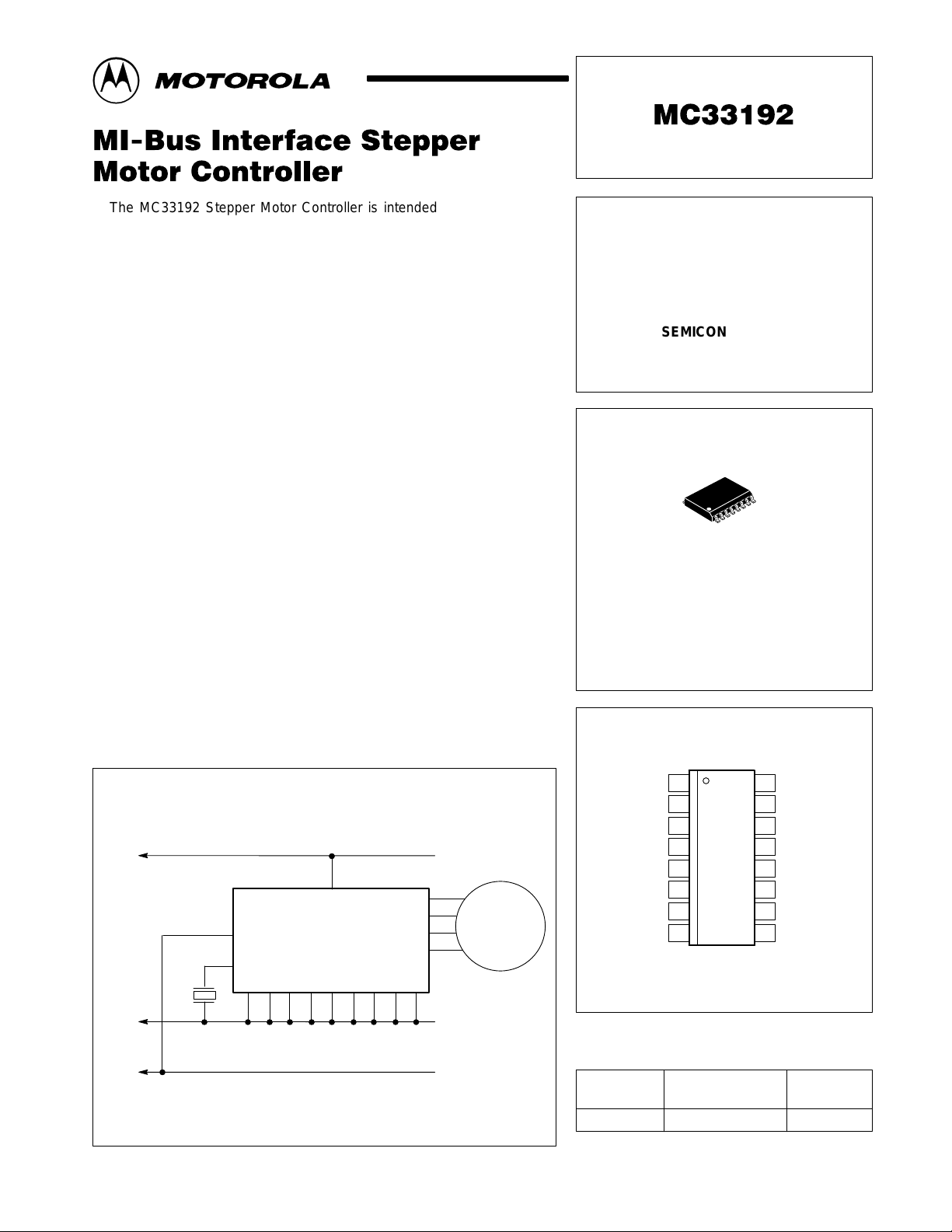
Simplified Application
7
V
CC
1
To
Other
Devices
MI–Bus
MI
8
Xtal
16 15 14 13 12 1 1 10 9 2
Ceramic
Resonator
This device contains 1,528 active transistors.
MC33192DW
MOTOROLA ANALOG IC DEVICE DATA
A1
A2
B1
B2
Gnd
+V
batt
3
4
5
6
Ground
From MCU
MI–Bus
Stepper
Motor
PIN CONNECTIONS
15
14
13
12
11
10
Gnd
Gnd
Gnd
Gnd
Gnd
Gnd
Gnd
Gnd
9
MI–Bus
Gnd
A1
A2
B1
B2
V
CC
Xtal
116
2
3
4
5
6
7
8
(Top View)
ORDERING INFORMATION
Operating
Device
MC33192DW TA = – 40° to +100°C
Motorola, Inc. 1996 Rev 0
Temperature Range
Package
SO–16L
1
Page 2
MC33192
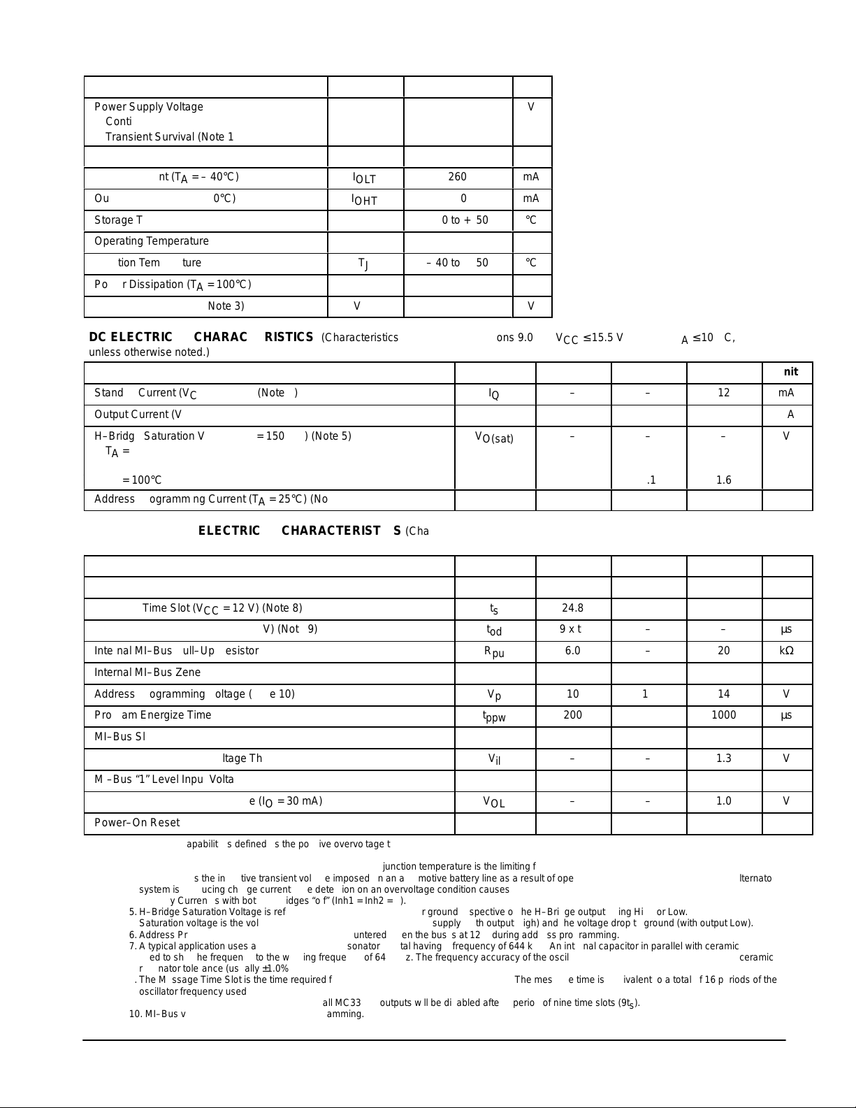
MAXIMUM RATINGS
(All voltages are with respect to ground, unless otherwise noted.)
Rating Symbol Value Limit
Power Supply Voltage
Continuous Operation V
Transient Survival (Note 1) V
Digital Input Voltage
Output Current (TA = – 40°C)
Output Current (TA = 100°C)
Storage Temperature
Operating Temperature (Note 2)
Junction Temperature
Power Dissipation (TA = 100°C)
Load Dump Transient (Note 3)
CC
V
I
OLT
I
OHT
T
stg
T
T
P
V
LD
i
A
J
D
LD
25
40
0.3 to VCC + 0.3
260
150
– 40 to +150
– 40 to +125
– 40 to +150
0.5
40
DC ELECTRICAL CHARACTERISTICS (Characteristics noted under conditions 9.0 V ≤ V
V
V
mA
mA
°C
°C
°C
W
V
≤ 15.5 V, – 40°C ≤ TA ≤ 100°C,
CC
unless otherwise noted.)
Characteristic
Standby Current (VCC = 15.5 V) (Note 4)
Output Current (VCC = 15.5 V)
H–Bridge Saturation Voltage (IO = 150 mA) (Note 5)
Symbol Min Typ Max Unit
V
O(sat)
I
Q
I
O
–
–
–
–
120
–
TA = – 40°C – 1.3 1.6
TA = 25°C – 1.2 1.6
TA = 100°C – 1.1 1.6
Address Programming Current (TA = 25°C) (Note 6)
I
pc
–
1.2
12
mA
–
–
–
mA
V
A
CONTROL LOGIC ELECTRICAL CHARACTERISTICS (Characteristics noted under conditions 9.0 V ≤ V
≤ 15.5 V, – 40°C ≤ TA ≤
CC
100°C, unless otherwise noted.)
Characteristic
Oscillator (Note 7)
Message Time Slot (VCC = 12 V) (Note 8)
Urgent Output Disable (VCC = 12 V) (Note 9)
Internal MI–Bus Pull–Up Resistor
Internal MI–Bus Zener Diode Clamp Voltage
Address Programming Voltage (Note 10)
Program Energize Time
MI–Bus Slew Rate
MI–Bus “0” Level Input Voltage Threshold
MI–Bus “1” Level Input Voltage Threshold
MI–Bus “0” Level Output Voltage (IO = 30 mA)
Power–On Reset Time (VCC ≥ 7.5 V)
NOTES: 1. Transient capability is defined as the positive overvoltage transient with 250 ms decay time constant. The detection on an overvoltage condition causes all
H–Bridges to be latched “off”.
2.Ambient temperature is given as a convience; Maximum junction temperature is the limiting factor.
3.Load Dump is the inductive transient voltage imposed on an automotive battery line as a result of opening the battery connection while the alternator
system is producing charge current. The detection on an overvoltage condition causes all H–Bridges to be latched “off”.
4.Standby Current is with both H–Bridges “off” (Inh1 = Inh2 = 0).
5.H–Bridge Saturation V oltage is referenced to the positive supply or ground respective of the H–Bridge output being High or Low.
Saturation voltage is the voltage drop from the output to the positive supply (with output High) and the voltage drop to ground (with output Low).
6.Address Programming Current is the current encountered when the bus is at 12 V during address programming.
7.A typical application uses an external ceramic resonator crystal having a frequency of 644 kHz. An internal capacitor in parallel with ceramic resonator is
used to shift the frequency to the working frequency of 640 kHz. The frequency accuracy of the oscillator is dependant on the capacitor and ceramic
resonator tolerance (usually ±1.0%).
8.The Message Time Slot is the time required for one complete device message transfer. The message time is equivalent to a total of 16 periods of the
oscillator frequency used.
9.If the MI–Bus becomes shorted to ground, all MC33192 outputs will be disabled after a period of nine time slots (9ts).
10. MI–Bus voltage required for address programming.
Symbol Min Typ Max Unit
f
cl
t
s
t
od
R
pu
V
cl
V
p
t
ppw
∆V/∆t
V
il
V
ih
V
OL
t
por
24.8
9 x t
6.0
–
10
200
1.0
–
2.4
–
–
s
640
25
–
–
18
12
1.5
–
–
–
250
–
25.2
–
20
–
14
1000
2.0
1.3
–
1.0
–
kHz
µs
µs
kΩ
V
V
µs
V/µs
V
V
V
µs
2
MOTOROLA ANALOG IC DEVICE DATA
Page 3
MC33192
GENERAL DESCRIPTION
The MC33192 is a serial stepper motor controller for use in
harsh automotive applications using multiplex wiring. The
MC33192 provides all the necessary four phase drive signals
to control two phase bipolar stepper motors operated in either
half or full step modes. Multiple stepper motor controllers can
be operated on a real time basis at step frequencies up to
200 Hz using a single microcontroller (MCU). A primary
attribute of operation is the utilization of the MI–Bus message
media to provide high noise immunity communication
ensuring very high operating reliability of motor stepping.
The MC33192 is designed to drive bipolar stepper motors
having a winding resistance of 80 Ω at 20°C with a supply
voltage of 12 V. It is supplied in a SO–16L plastic package
having eight pins, on one side, connected directly to the lead
frame thus enhancing the thermal performance to allow a
power dissipation of 0.5 W at 120°C ambient temperature.
Multiple Simultaneous Motor Operation
Several motors can be controlled in a serial fashion, one
after the other, using the same software time base. The time
base determines the step frequency of the motors. A single
motor can be operated at a maximum speed of 200 Hz
pull–in with a duration of 5.0 ms per step. Three motors can
be operated simultaneously using a 68HC05B6 MCU at the
same time base (200 Hz) with about 1.7 ms per step. A
68HC11 MCU can control 4 stepper motors with adequate
program step time. The step frequency must be decreased to
control additional motors. To control eight motors
simultaneously would require the motor speed to be
decreased to 100 Hz producing about 2.0 ms time duration
per step with adequate program time.
MI–Bus General Description
The Motorola Interconnect Bus (MI–Bus) is a serial
push–pull communications protocol which efficiently
supports distributed real time control while exhibiting a high
level of noise immunity .
Under the SAE Vehicle Network categories, the MI–Bus is
a Class A bus with a data stream transfer bit rate in excess of
20 kHz and thus inaudible to the human ear. It requires a
single wire to carry the control data between the master MCU
and its slave devices. The bus can be operated at lengths up
to 15 meters.
At 20 kHz the time slot used to construct the message
(25 µs) can be handled by software using many MCUs
available on the market.
The MI–Bus is suitable for medium speed networks
requiring very low cost multiplex wiring. Aside from ground,
the MI–Bus requires only one signal wire connecting the
MCU to multiple slave MC33192 devices with individual
control.
A single MI–Bus can accomplish simultaneous automotive
system control of Air Conditioning, Head Lamp Levellers,
Window Lifts, Sensors, Intelligent Coil Drivers, etc. The
MI–Bus has been found to be cost effective in vehicle body
electronics by replacing the conventional wiring harness.
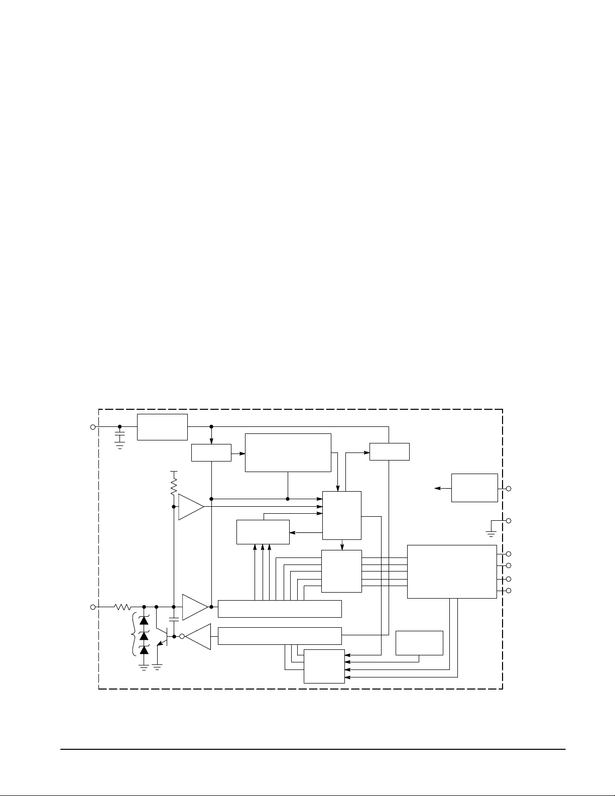
Figure 1 shows the internal block diagram of the MC33192
Stepper Motor Controller.
Xtal (8)
MI (1)
Oscillator
(640 kHz)
10 k
Programming
Level Detection
Ω
20
18 V
Figure 1. MC33192 Stepper Motor Conroller Block Diagram
5.0 V
Divider
Noise Detector
Bi–Phase
Bi–Phase Program
Programmed
Address
Serial to Parallel Register
Parallel to Serial Register
Status
Encoder
Control
Logic
Latch
Divider
20 kHz
5.0 V
Dual Bridge Driver and
Motor Diagnostics
Thermal
Shutdown
Regulator
5.0 V
+VCC (7)
Gnd (*)
A11 (3)
A12 (4)
B11 (5)
B12 (6)
NOTE: (*) Pins 2, 9, 10, 11, 12, 13, 14, 15 and 16 are common electrical and heatsink ground pins for the device.
MOTOROLA ANALOG IC DEVICE DATA
3
Page 4
MC33192
ÁÁ
ББББББББ
ÁÁ
ББББББББ
ÁÁ
ББББББББ
ÁÁ
ББББББББ
ÁÁ
ББББББББ
ÁÁ
ББББББББ
ÁÁ
ББББББББ
ÁÁ
ББББББББ
ÁÁ
Á
Á
ББББББББ
Á
MI–Bus Access Method
The information on the MI–Bus is sent in a fixed message
frame format (See Figure 4). The system MCU can take
control of the MI–Bus at any time with a start bit which
violates the law of Manchester Bi–Phase code by having
three consecutive Time Slots (3ts) held constantly at a Logic
“0” state.
Push–Pull Communication Sequence
Communication between the system MCU and slave
MC33192 devices always use the same message frame
organization. The MCU first sends eight serial data bits over
the MI–Bus comprised of five control bits followed by three
address bits. This communication sequence is called a “Push
Field” since it represents command information sent from the
MCU. The sequence of the five control data bits follow the
order D0, D1, D2, D3 and D4. The three address bits are sent
in sequential order A0, A1 and A2 defining a binary address
code. The condition of MI–Bus during any of the control bit
time windows defines a specific control function as shown in
Figure 2. A “Pull Sync” bit is sent at the end of the Push Field,
the positive edge of which causes all data sent to the
selected device to be latched into the output circuit.
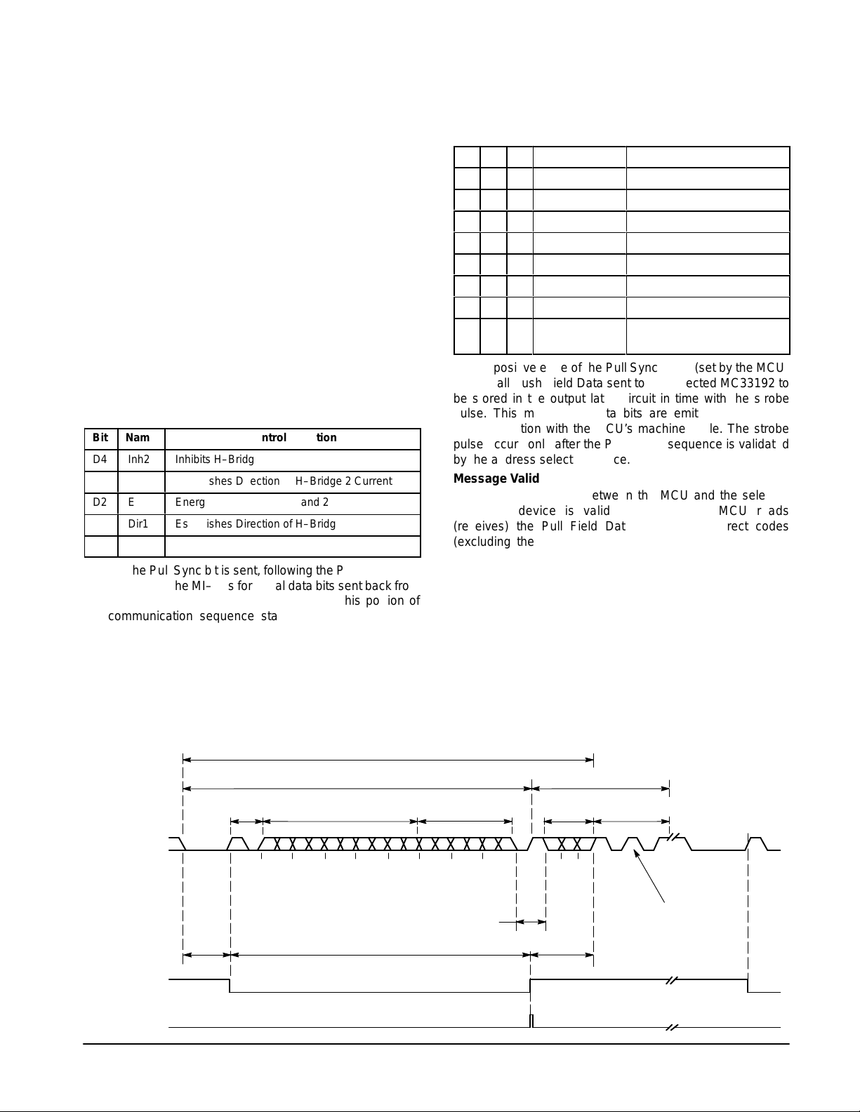
Figure 2. Push Field Data Bits
Bit
D4
D3
D2
D1
D0
Name
Inh2
Dir2
E
Dir1
Inh1
Inhibits H–Bridge 2
Establishes Direction of H–Bridge 2 Current
Energizes Bridge Coils 1 and 2
Establishes Direction of H–Bridge 1 Current
Inhibits H–Bridge 1
Control Function
After the Pull Sync bit is sent, following the Push Field, the
MCU listens on the MI–Bus for serial data bits sent back from
the previously addressed MC33192 device. This portion of
the communication sequence starts the “Pull Field Data”
since it represents information pulled from the addressed
MC33192 and received by the MCU.
The address selected MC33192 device sends data, in
the form of status bits, back to the MCU reporting the
devices condition. At the end of the Push Field the MCU
outputs a Pull Sync bit which signals the start of the Pull
Field. In the Pull Field are three bits (S2, S1 and S0) which
report the status of the previously addressed MC33192
according to Figure 3.
Figure 3. Pull Field Status Bits
S2
S1
Á
S0
0
0
0
0
0
1
0
1
0
0
1
1
1
0
0
1
0
1
1
1
0
1
1
1
Status
Not used
Free
No Back EMF
Free
Normal/OK
Thermal
Programming
Selection failed
ÁÁÁÁ
Comments
Drivers and/or coils failed
Chip temperature > 150°C
PROM energized
Noise on MI–Bus, failed or
БББББББ
disconnected module
The positive edge of the Pull Sync pulse (set by the MCU)
causes all Push Field Data sent to the selected MC33192 to
be stored in the output latch circuit in time with the strobe
pulse. This means the data bits are emitted in real time
synchronization with the MCU’s machine cycle. The strobe
pulse occurs only after the Push Field sequence is validated
by the address selected device.
Message Validation
The communication between the MCU and the selected
MC33192 device is valid only when the MCU reads
(receives) the Pull Field Data having the correct codes
(excluding the code “1–1–1” and “0–0–0”) followed by an
End–of–Frame signal. The frequency of the End–of–Frame
signal may be a sub–multiple of the selected devices local
oscillator or related to an internal or external analog
parameter using a Voltage to Frequency Converter.
Error Detection
An error is detected when the Pull Field contains the code
“1–1–1” followed by the End–of–Frame permanently tied to a
logic “1” state (internally from 5.0 V through a pull–up
resistor). This means the communication between the MCU
and the selected device was not obtained.
MI–Bus Wire
Push/Pull Function
Strobe
4
Figure 4. MI–Bus Timing Diagram
Frame
Push Field
AddressDataPush Sync Data End–of–Frame
3t
s
234567891 1 32
“0” S1
“1”D3
S2 S0
NRZ
Bi–Phase Coded
Pull Sync
Coded
75 µs 475 µs 100 µs
Push
Strobe Pulse
MOTOROLA ANALOG IC DEVICE DATA
Pull Field
4
÷
32 = 20 kHz
Pull
Oscillator
Frequency
3t
s
StartStart “1” “0” D0 D1 D2 D4 A0 A1 A2
Page 5

MC33192
There are four types of system error detections which are
not mutually exclusive; These are:
1) Noise Detection
The system MC33192 slave devices receive the Push
Field message from the MCU twice for each Time Slot (ts)
of the Bi–Phase Code. A receive error occurs when the two
message samples fail to “logic wise” match. Noise and
Bi–Phase detection are discussed further under Message
Coding.
2) Bi–Phase Detection
The system slave devices receiving the Push Field
message from the MCU detect the Bi–Phase Code. A
detector error occurs when the two time slots of the Bi–Phase
Code do not contain an Exclusive–OR logic function.
3) Field Check
A field error is detected when a fixed–form bit field
contains an improper number of bits. A bit error can also be
detected by the MCU during the Push Field. The MCU can
simultaneously monitor the MI–Bus at the time it is sending
data. A bit error is detected if the sent bit value does not
match the value which was monitored.
4) Urgent Output Disable
If the MI–Bus becomes shorted to ground, the slave
device outputs will be disabled after a period of 9ts. The MCU
itself can take advantage of this feature to “globally” disable
the outputs of all system slave devices by keeping the
MI–Bus at a logic “0” level for a duration of 9ts or more.
Normal operation is resumed when the MCU sends a
“standard” instruction over the MI–Bus.
Basic Stepper Motor Construction and Operation
Stepper motors are constructed with a permanent magnet
rotor magnetized with the same number of pole pairs as
contained in one stator coil section. Operationally, stepper
motors rotate at constant incremental angles by stepping one
step every time the current switches discretely in one stator
field coil causing the North–South stator field to rotate either
clockwise or counter–clockwise causing the permanent
magnet rotor to follow (see Figure 5). For simplicity, assume
the starting condition of the A1 to A2 stator field to be top to
bottom polarized N to S and the B1 to B2 stator field to be left
to right polarized N to S. The resulting stator field will produce
a vector which points in the direction of position 3. The rotor
will, in this case, be in the position shown in Figure 5 (pointing
to position 1). This initial condition corresponds to that of
step 1 in Figure 6. As the direction of current flow in the B1 to
B2 stator field is reversed, the field polarity of the B1 to B2
also reverses and is left to right polarized S to N. This causes
the resulting stator field vector to point in the direction of
position 4. This in turn causes the N–S rotor to follow and
rotate 90° in a clockwise direction and point in the direction of
position 2. This condition corresponds to step 2 of Figure 6.
Continued clockwise rotor steps will be experienced as the
stator field continues to be incrementally rotated as shown in
steps 3, 4, 5, etc. of Figure 6. The 90° steps in this simplistic
example constitute “full steps”. It is to be noticed that both
coils, in the foregoing full step example, were simultaneously
energized in one of two directions. It is possible to increment
the rotor in 45° “intermediate steps” or “half steps” by
alternately energizing only one stator coil at a time in the
appropriate direction while turning the other stator coil off.
The drive signals for Half Step operation are shown in
Figure 7. The Power output stages of the MC33192 consist
of two H–Bridges capable of driving two–phase bi–polar
permanent magnet motors in either half or full step
increment.
Figure 5. Permanent Magnet Stepper Motor
A1
3
B1 B2
2
A2
4
1
Figure 6. 4–Step “Full Step” Operation
Step
Coil A
(A1 to A2)
Coil B
(B1 to B2)
Stator
Field
Rotor
Position
Rotor
Direction
1234 56
+
–
+
–
CWCCW
Figure 7. 8–Step “Half Step” Operation
Step
Coil A
(A1 to A2)
Coil B
(B1 to B2)
Stator
Field
Rotor
Position
Rotor
Direction
123456
+
–
+
–
781
CWCCW
MOTOROLA ANALOG IC DEVICE DATA
5
Page 6

MC33192
Permanent magnetic stepping motors exhibit the
characteristic ability to hold a shaft rotor position with or
without a stator coil being energized. Normally the shaft
holding ability of the motor with a stator coil energized is
referred to as “Holding Torque” while “Residual Torque” or
“Detent Torque” refers to the shaft holding ability when a
stator coil is not energized. The Holding Torque value is
dependent on the interactive magnetic force created by the
resulting energized stator fields with that of the permanent
magnet rotor. The Residual Torque is a function of the
physical size and composition of the permanent magnet rotor
material coupled with its intrinsic magnetic attraction for the
un–energized stator core material and as a result, the weaker
of the two torques.
It is to be noted when using half step operation, only one
coil is energized during alternate step periods which
produces a somewhat weaker Holding Torque. Holding
Torque is maximized when both coils are simultaneously
Figure 8. Truth Table and Serial Push Field Data Bits For Sequential Stepping
Push Field Bits
Step
Full Half
D0 D1
Inh1
DIR1
D2ED3
DIR2D4Inh2 A1 A2 B1 B2
energized. In addition, since each winding and resulting flux
conditions are not perfectly matched for each half step,
incremental accuracy is not as good as when full stepping.
T wo Phase Drive Signals
The DIR1 and DIR2 bits in the Data Frame of the Push
Field determine the direction of H–Bridge current flow, and
thus the magnetic field polarization of the stator coils, for
H–Bridge outputs “A” and “B” respectively. The directional
signals DIR1 and DIR2, generated by the MCU,
communicate over the MI–Bus to control the two H–Bridge
power output stages of the MC33192 to drive two phase
bipolar permanent magnet motors. Figure 8 shows the
MC33192 truth table to accomplish incremental stepping of
the motor in a clockwise or counter–clockwise direction in
either half or full step modes. The stator field polarization and
rotor position are also shown for reference relative to the
basic stepper motor of Figure 5.
H–Bridge Outputs
Stator
Field
(Note 2)
Rotor
Position
(Note 2)
Direction
of Shaft
Rotation
1
1
101011010
–
2
101X010ZZ
2
3
101111001
–
4
0X 1 1 1 ZZ01
3
5
111110101
–
6
111X00100
7
4
–
NOTES: 1. X = Don’t care; Z = High impedance; 1 = High (active “on”) state; 0 = Low (inactive “off”) state.
111010110
8
0X 1 0 1 ZZ10
0XXX0ZZZZ
11011Z1Z1
100011Z1Z
11000Z1ZZ
00011ZZZ1
2.The stator field direction and position of the rotor are shown for explanation purposes and relative to the basic
stepper motor shown in Figure 3.
3.DIR1 establishes the direction of current flow in H–Bridge “A”.
4.DIR2 establishes the direction of current flow in H–Bridge “B”.
CCW
CW
6
MOTOROLA ANALOG IC DEVICE DATA
Page 7

MC33192
MI–Bus Interface Description
The MI–Bus Interface shown in Figure 9 is made up of a
single NPN transistor (Q1). The two main functions of this
NPN transistor are:
1) To drive the MI–Bus during the Push Field with
approximately 20 mA of current while also exhibiting low
saturation characteristics (V
CE(sat)
).
2) To protect the Input/Output (I/O) pin of the MCU against
any Electro–Magnetic Interference (EMI) captured on the
bus wire.
Without the NPN transistor, the MCU could be destroyed
as a result of receiving excessive EMI energy present on the
bus. In addition, the transistor blocks the MCU from receiving
EMI signals which could erroneously change the data
direction register of the MCU I/O.
The MCU input pin (Pin), used to read the Pull Field of the
MI–Bus, is protected by two diodes (D2 and D3) and two
resistors (R5 and R6). Any transient EMI generated voltage
present on the bus is clamped by the two diodes to a
windowed voltage value not to be greater than the VDD or
less than the VSS supply voltages of the MCU.
MI–Bus Levels
The MI–Bus can have one of two valid logic states,
recessive or dominant. The recessive state corresponds to a
Logic “1” and is obtained through use of a 10 kΩ pull–up
resistor (R9) to 5.0 V. The dominant state corresponds to a
Logic “0” which represents a voltage less than 0.3 V and
created by the V
CE(sat) of Q1.
MI–Bus Overvoltage Protection
An external zener diode (Z1) is incorporated in the
interface circuit so as to protect the MCU output pin (P
out
from overvoltages commonly encountered in automotive
applications as a result of “Load Dump” and “Jump Start”
conditions. Load Dump is defined as the inductive transient
generated on the battery line as a result of opening the
battery connection while the alternator system is producing
charge current. Jump Start overvoltages are the result of
paralleling the installed automotive battery, through the use
of “jumper cables”, to an external voltage source in excess
of the vehicles nominal system voltage. For 12 V
automotive systems, it is common for 24 V “jump start”
voltages to be used.
When an overvoltage situation (>18 V) exists, due to a
load dump or jump start condition, the zener diode (Z1) is
activated and supplies base current to turn on the NPN
transistor Q1 causing the bus to be pulled to less than 0.3 V
producing a Logic “0” on the MI–Bus. After a duration
corresponding to 8ts (200 µs) of continuous Logic “0” on the
bus all MC33192 devices will disable their outputs. Normal
operation is resumed, following the overvoltage, by the MCU
sending out a “standard” message instruction.
MI–Bus T ermination Network
The MI–Bus is resistively loaded according to the number
of MC33192 devices installed on the bus. Each MC33192
has an internal 10 kΩ pull–up resistor to 5.0 V. An external
pull–up resistor (R7) is recommended to be used to optimally
adjust termination of the bus for a load resistance of 600 Ω.
)
5.0 V
V
DD
MCU
V
SS
Figure 9. MI–Bus MCU Interface
Program
Run
Z1
R1
(4.7 K)
P
out
D1
R5
P
(10 k)
in
(18 V)
R3
(3.9 k)
V
DD
D2
D3
R2
(1.2 k)
MI–Bus
Q1
R4
(10 k)
R6
(22 k)
5.0 V
Z
in
R7
(1.2 k)
#2
#3
#4
#5
#6
#7
#8
R8
Ω
)
(20
1
Z2
(18 V)
Additional MC33192 Devices
5.0 V
MC33192
6.5 V
R9
(10 k)
Q2
Data
Out
7
V
Gnd
2
CC
12 V
Programming
Data In
0 V
MOTOROLA ANALOG IC DEVICE DATA
7
Page 8

MC33192
MESSAGE CODING
Bi–Phase Coding and Detection
The Manchester Bi–Phase code shown in Figure 10
requires two time slots (2ts) to encode a single data bit. This
allows detection of a single error at the time slot level. The
logic levels “1” or “0” are determined by the organization of
the two time slots. These always have complementary logic
levels of either zero volts or plus five volts, which are
detected using an Exclusive OR detection circuit during the
Push Field sequence. A “1” bit is detected when the first time
slot is set to a zero logic state (0 V) followed by the second
time slot set to a logic state one (5.0 V). Conversely , a “0” bit
is detected when the first time slot is set to the logic state
“one” (5.0 V) followed by a second time slot set to a “zero”
logic state (0 V). For these two bits are Exclusive–ORs of
each other.
The addressed devices receiving the Push Field detect
the Bi–Phase code. Bi–Phase detection involves the
sampling of the Push Field Bi–Phase code twice (a and b) for
each time slot. A code error occurs when the two time slots of
the Bi–Phase do not follow a logical Exclusive–OR function
(see Figure 10).
Noise monitoring is accomplished by sampling the Push
Field Bi–Phase code twice (a and a’) and (b and b’) during
each time slot. A noise error is detected if the two sample
values do not have the same logical level.
Figure 10. Noise/Bi–Phase Detection
2 t
s
5.0 V
Push Field
Bi–Phase
Coded Bits
t
s
(Logic “0”)
001234567 12345670
abab
ababa’ b’ a’
t
s
(Logic “1”)
b’
t
Bi–Phase
Detection
Noise
Detection
Each message frame consists of two fields: The Push
Field, in which data and addresses are transferred by the
MCU to the slave device; and the Pull Field, in which serial
data is transferred back to the MCU from the address
selected slave device. The message frame is broken down
into seven individual field segments as indicated in Figure 4
(Start, Push Field Sync, Push Field Data, Push Field
Address, Pull Field Sync, Pull Field Data, and
End–of–Frame). The following lists the bit size and function
of each of these segments:
1) Start is the start of message and consists of three time
slots (3ts) having the dominant Logic “0” state of less than
0.3 V . Holding the MI–Bus at ground for three time slots (3ts)
marks the beginning of the message frame by violating the
law of the Manchester Code.
2) Push Field Sync is a single bit which establishes initial
timing for the Push Field Data to follow.
3) Push Field Data is comprised of five serial data bit
fields (D0, D1, D2, D3 and D4) which comprise the instruction
set defining the configuration and condition of the two
H–Bridge output stages.
4) Push Field Address is comprised of three serial data
bit fields (A0, A1 and A2) which define the address or name
of a MC33192 on the MI–Bus.
5) Pull Field Sync is a single bit which establishes the end
of the Push Field and the initial start timing for the Pull Field
Data to follow.
6) Pull Field Data is made up of three serial data bit fields
(S2, S1 and S0) which contain the existing status information
of an addressed MC33192.
7) End–of–Frame field is a signal which communicates
to the MCU that the status information sent by the MC33192
is complete.
The Push Field Sync bit, Push Field Data bits, Push Field
Address bits, Pull Field Sync bit are all coded by the
Manchester Bi–Phase L Code. The Pull Field Data bits are
Non–Return to Zero (NRZ) coded. The End–of Frame field is
a square wave signal with a frequency of 20 kHz or higher so
as to avoid a condition which causes a bus violation.
The Manchester Bi–Phase L code requires two time slots
(2ts) to encode a single bit. This allows a single error to be
detected during the time slot.
Address Programming involves the use of three
instructions. Refer to Figure10.
First Instruction Set the MI–Bus continuously at 12 V.
This places the MC33192 in the programming mode.
Programming is possible only when the MI–Bus is at 12 V.
Next, the MCU serially enters ”Logic Zeros” in all five Push
Field Data bit positions (D0, D1, D2, D3 and D4) followed by
the designated address value in the Push Field Address
positions (A0, A1, & A2).
The MCU now waits 275 µs before starting the second
instruction. The total of the Pull time, Delay time, and Bus
Violation time (V) of the second instruction (150 µs, 275 µs
and 75 µs respectively) will cause the memory cell to be
energized for 500 µs. During the first 150 µs of this time, the
MCU is checking the Pull Field Data Bits S2, S1 and S0
looking for the programming code “110” to indicate
complete activation of the memory cell.
Second Instruction (MI–Bus voltage remaining at 12 V)
The MCU repeats the same Push Field instruction as
previously sent in the First Instruction; entering all “Logic
Zeros” in the Push Field Data positions followed by the
designated Push Field Address value in the address
positions.
Again, the MCU waits for the Pull, Delay, and Bus violation
time while checking the Pull Field Data bits looking for the
programming code “110” code. The MCU must repeat the
initial Push Field Address instruction until a “110” code is
received before advancing to the Third Instruction.
Third Instruction The MI–Bus voltage is lowered to 5.0 V .
The MCU serially loads “Logic Zeros” in all five Push Field
Data bit positions followed by the programmed address in the
Push Field Address positions. The MCU then checks the Pull
Field Address status bits looking this time for the
8
MOTOROLA ANALOG IC DEVICE DATA
Page 9

MC33192
programming OK code “100” indicating the address
programming to be executed.
The First and Second Instructions must be repeated until
the MCU successfully receives the programming code
“100”. Address programming is not complete until a “100”
OK status is received by the MCU with the MI–Bus voltage
at 5.0 V.
Overwrite–Bit Programming involves the use of two
instructions. See Figure 1 1.
First Instruction Have the MI–Bus continuously set at
12 V so as to have the MC33192 in the programming mode.
Programming can only be accomplished with the MI–Bus at
12 V.
The MCU serially enters “Logic Zeros” for the Push Field
Data bits D0, D1, D2 and D3 and a Logic “1” for D4 bit
followed by the programmed address bits A0, A1 and A2.
The MCU now waits 275 µs before starting the second
instruction. The total of the Pull time, Delay time, and Bus
Violation time (V) of the second instruction (150 µs, 275 µs
and 75 µs respectively) will cause the memory cell to be
energized for 500 µs. During the first 150 µs of this time, the
MCU is checking the Pull Field Data Bits for the status of bits
S2, S1 and S0 looking for the programming code “110” to
indicate complete activation of the memory cell.
Second Instruction (MI–Bus remaining at 12 V)
The MCU repeats the first instruction outlined above until
the programming OK code “100” is sent back to the MCU
from the selected MC33192 indicating the overwrite–bit
protection to be programmed. If after eight repeat
instructions, the programming code “110” or the OK code
“100” is not generated four times in succession,
programming of the MC33192 has failed. If this occurs, the
Overwrite–Bit Programming sequence should be reviewed
and re–started from the beginning.
H–Bridge Output
The H–Bridge output drive circuit and associated
diagnostic encoder are shown in Figure 12. The H–Bridge
output uses internal diode clamps (D1, D2, D3, D4) to provide
transient protection of the output transistors necessary when
switching inductive loads associated with stepper motors.
Back EMF Detection
Three different Back EMF currents can occur depending
on whether the motor is running or manner in which it is being
stopped. Referring to Figure 12; When the Dir1 bit is set to
logic 0, the direction of current flow will be from VCC through
transistor Q2, Coil A (A1 to A2), and transistor Q4 to ground.
1) Fast Decay (when transistors Q1, Q2, Q3 and Q4 are
switched off).
When the current flowing in the coil is stopped by setting
the Inh1
bit to logic 0, the back EMF current will circulate
through the voltage supply (VCC) and diodes D1 and D3. At
that time, the voltage developed across the diode D1 is
detected by transistor Q6. The generated voltage pulse of Q6
is then encoded and sent, in the Pull–Field, to the
microprocessor.
2) Slow Decay (Q3 and Q4 are switched off)
When the current flowing in the coil is stopped by setting
the E bit to logic 0, the back EMF current will circulate through
the diode D1 and transistor Q2 which is already switched on.
3) When Motor is Running
The rotational direction of the motor changes whenever
the Dir bit state is changed. When the Dir bit is changed from
a logic 0 to a logic 1, transistors Q2 and Q4 are switched off
and transistors Q1 and Q3 are switched on. At this time, the
back EMF current will circulate from ground through diodes
D1 and D3 to the voltage supply (VCC). In all cases, the back
EMF currents will be detected by transistors Q5 and Q6.
Programming
MI–Bus Voltage
Instruction Number
MI–Bus Field
Status Code
Overwrite–Bit
Status Code
Strobe Pulse
Memory Cell
Figure 11. Address Programming Diagram
Active
Finished Finished
12V
5.0 V
Address
Energy in
1
Push Pull DelayV V Pull Delay VPush Push Pull
µ
s 150 µs 275 µs 75 µs 550 µs
550
“110” “110”
500
µ
s
2
150 µs 275 µs 75 µs
“100”“110”
500 µs475 µs
12 V
5.0 V
3
“100”
“100”
OK
t
MOTOROLA ANALOG IC DEVICE DATA
9
Page 10

Inh1
MC33192
Figure 12. H–Bridge Output Drive Circuit and Diagnostic Encoder
V
CC
Dir 1
EE
BF1
BF2
ST
Programming
Thermal
Q2
Q3
D2
D3
DQ
C
Q5 Q6
D1
D4
Q1
Q4
A1
Coil 1
A2
Ground
S0
S1
S2
B1
Coil 2
B2
S2 S1 S0 Status
000
001
010
011
100
101
110
111
Second
H–Bridge
Not Used
Free
No Back EMF
Free
Normal/OK
Thermal
Programming
Selection Failed
Inh2
Dir2
E
10
MOTOROLA ANALOG IC DEVICE DATA
Page 11

MC33192
Figure 13. Single Wire MI–Bus Control of 8 Stepper Motors
12 V
5.0 V
Regulator
Micorcontroller
MC68HC05B6
MC68HC11KA
Gnd
Program
Run
R2
R1
P
out
D1
P
R5
in
Z1
D2
D3
R3
Q1
R4
R6
Mi–Bus
MC33192DW
MC33192DW
MC33192DW
MC33192DW
MC33192DW
MC33192DW
Stepper
Motor
1
Stepper
Motor
2
Stepper
Motor
3
Stepper
Motor
4
Stepper
Motor
5
Stepper
Motor
6
MC33192DW
MC33192DW
Stepper
Motor
7
Stepper
Motor
8
MOTOROLA ANALOG IC DEVICE DATA
11
Page 12

–A–
16 9
D16X
M
0.010 (0.25) B
A
T
G14X
–B– P8X
81
S
S
C
K
MC33192
OUTLINE DIMENSIONS
DW SUFFIX
PLASTIC PACKAGE
CASE 751G–02
(SO–16L)
ISSUE A
M
0.010 (0.25)
–T–
SEATING
PLANE
J
B
F
M
NOTES:
1. DIMENSIONING AND TOLERANCING PER ANSI
Y14.5M, 1982.
2. CONTROLLING DIMENSION: MILLIMETER.
M
R
X 45
_
3. DIMENSIONS A AND B DO NOT INCLUDE MOLD
PROTRUSION.
4. MAXIMUM MOLD PROTRUSION 0.15 (0.006) PER
SIDE.
5. DIMENSION D DOES NOT INCLUDE DAMBAR
PROTRUSION. ALLOWABLE DAMBAR
PROTRUSION SHALL BE 0.13 (0.005) TOTAL IN
EXCESS OF D DIMENSION AT MAXIMUM
MATERIAL CONDITION.
DIM MIN MAX MIN MAX
A 10.15 10.45 0.400 0.411
B 7.40 7.60 0.292 0.299
C 2.35 2.65 0.093 0.104
D 0.35 0.49 0.014 0.019
F 0.50 0.90 0.020 0.035
G 1.27 BSC 0.050 BSC
J 0.25 0.32 0.010 0.012
K 0.10 0.25 0.004 0.009
M 0 7 0 7
____
P 10.05 10.55 0.395 0.415
R 0.25 0.75 0.010 0.029
INCHESMILLIMETERS
Motorola reserves the right to make changes without further notice to any products herein. Motorola makes no warranty , representation or guarantee regarding
the suitability of its products for any particular purpose, nor does Motorola assume any liability arising out of the application or use of any product or circuit, and
specifically disclaims any and all liability, including without limitation consequential or incidental damages. “T ypical” parameters which may be provided in Motorola
data sheets and/or specifications can and do vary in different applications and actual performance may vary over time. All operating parameters, including “Typicals”
must be validated for each customer application by customer’s technical experts. Motorola does not convey any license under its patent rights nor the rights of
others. Motorola products are not designed, intended, or authorized for use as components in systems intended for surgical implant into the body, or other
applications intended to support or sustain life, or for any other application in which the failure of the Motorola product could create a situation where personal injury
or death may occur. Should Buyer purchase or use Motorola products for any such unintended or unauthorized application, Buyer shall indemnify and hold Motorola
and its officers, employees, subsidiaries, affiliates, and distributors harmless against all claims, costs, damages, and expenses, and reasonable attorney fees
arising out of, directly or indirectly, any claim of personal injury or death associated with such unintended or unauthorized use, even if such claim alleges that
Motorola was negligent regarding the design or manufacture of the part. Motorola and are registered trademarks of Motorola, Inc. Motorola, Inc. is an Equal
Opportunity/Affirmative Action Employer.
How to reach us:
USA/EUROPE /Locations Not Listed: Motorola Literature Distribution; JAPAN: Nippon Motorola Ltd.; Tatsumi–SPD–JLDC, 6F Seibu–Butsuryu–Center,
P.O. Box 20912; Phoenix, Arizona 85036. 1–800–441–2447 or 602–303–5454 3–14–2 T atsumi Koto–Ku, Tokyo 135, Japan. 03–81–3521–8315
MFAX: RMF AX0@email.sps.mot.com – TOUCHT ONE 602–244–6609 ASIA/PACIFIC: Motorola Semiconductors H.K. Ltd.; 8B Tai Ping Industrial Park,
INTERNET: http://Design–NET.com 51 Ting Kok Road, Tai Po, N.T., Hong Kong. 852–26629298
12
◊
MOTOROLA ANALOG IC DEVICE DATA
M33192/D
*MC33192/D*
 Loading...