

Page 1
DUAL BIPOLAR OPERATIONAL AMPLIFIERS
.GOOD CONSUMPTION/SPEED RATIO :
ONLY 200µA/AmpFOR 2.1MHz,2V/µs
.SINGLE (OR DUAL) SUPPLY OPERATION
FROM +4V TO +44V (±2V TO ±22V)
.WIDE INPUT COMMON MODE VOLTAGE
RANGE INCLUDING V
.LOW LEVEL OUTPUT VOLTAGE CLOSE TO
-
: 100mVTYPICAL
V
CC
CC
-
.PIN TOPIN COMPATIBLE WITH STANDARD
DUAL OP AMPs
MC33172 - MC35172
LOW POWER
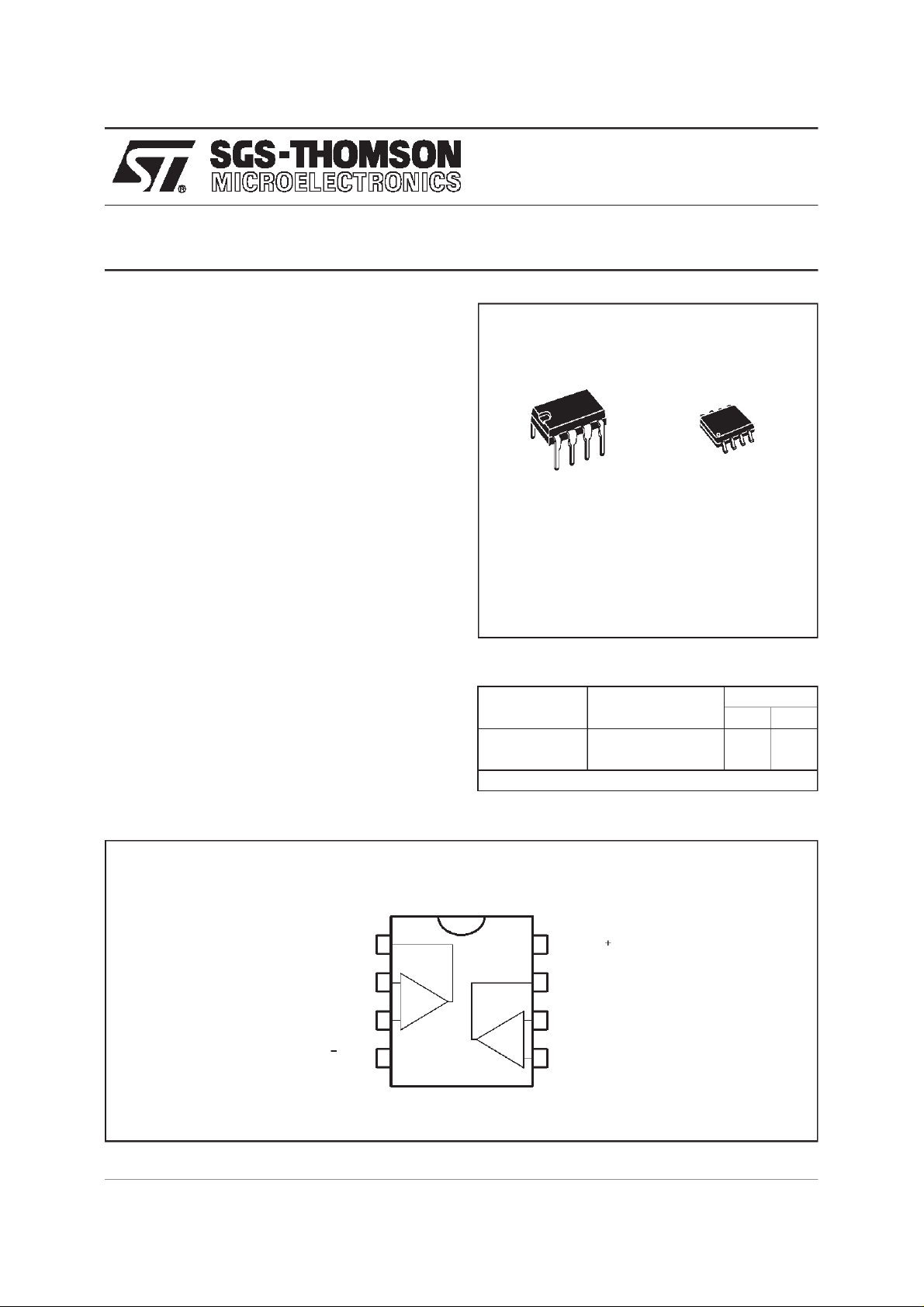
N
DIP8
(Plastic Package)
(Plastic Micropackage)
D
SO8
DESCRIPTION
The MC33172 series are dual bipolar operational
amplifiers offering both low consumption
(200µA/Amp)and good speed (2.1MHz,2V/µs).
Moreover the Input Common Mode Range
extends down to the lower supply rail, allowing
single supplyoperation from +4Vto +44V.
PIN CONNECTIONS (top view)
Output1
InvertingInput 1
Non-inverting Input 1
V
1
2
-
+
3
45
CC
ORDERCODES
Part Number Temperature Range
o
MC33172 -40
MC35172 -55
Example: MC33172N
V
8
CC
Ouptut
7
6
-
+
InvertingInput 2
Non-inverting Input 2
C, +105oC ••
o
C, +125oC ••
Package
ND
December 1997
1/5
Page 2
MC33172 - 35172
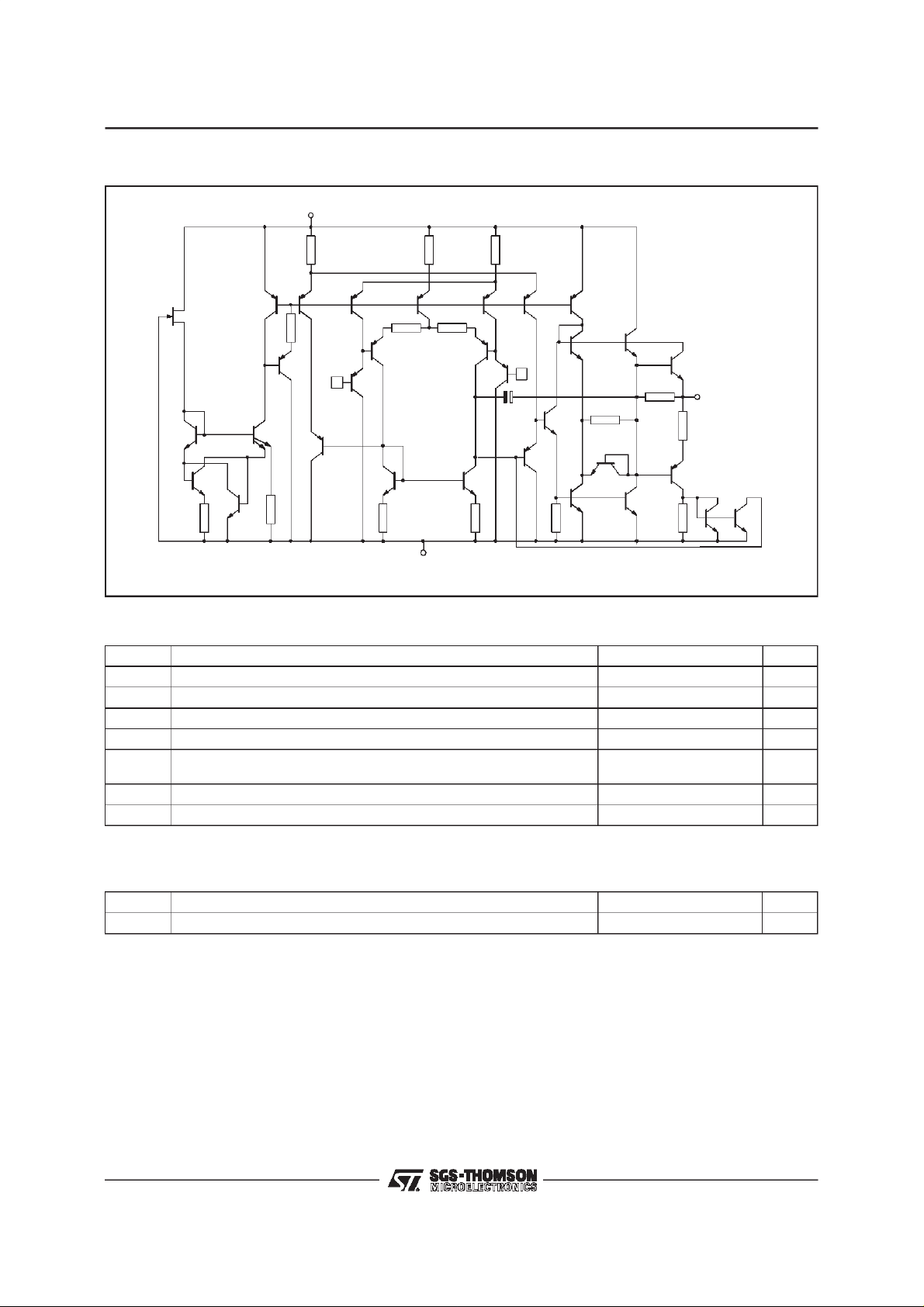
SCHEMATICDIAGRAM (for 1/2 MC33172)
V+
CC
T19
T15
R5
R7
R9
V-
CC
R4
T8
T1
T2
T3
R1
T7
T6
T5
T4
R2
T9
R3
Input -
T14
T13
T10 T11
R8
T16
T20
R10
R6
T22
R11
T24
T13
T23
R12
T27
T25
T29
R13
R14
R15
T26
T28
Output
T30
T31
T12
Input +
T17
C
T21
ABSOLUTEMAXIMUMRATINGS
Symbol Parameter Value Unit
V
V
T
T
Note 1: E ither or both input volt ages must not exceed the magnitu de of VCC.
Supply Voltage ±22 V
CC
Differential Input Voltage (Note 1) V
id
Input Voltage (Note 1) V
V
i
Output Short Circuit Duration Indefinite s
Operating Temperature Range MC33172
oper
T
Junction Temperature 150
j
Storage Temperature -65 to 150
stg
MC35172
-40 to 105
-55 to 125
o
C
o
C
o
C
OPERATINGCONDITIONS
Symbol Parameter Value Unit
V
2/5
Supply Voltage Range ±2to±22 V
CC
Page 3

MC33172 - 35172
ELECTRICAL CHARACTERISTICS
+
V
= +15V, V
CC
Symbol Parameter Min. Typ. Max. Unit
Input Offset Voltage
V
io
DV
A
V
V
V
Input Offset Voltage Drift 10 µV/oC
io
Input Offset Current (Vic= 0V)
I
io
I
Input Bias Current (Vic= 0V)
ib
Large Signal Voltage Gain (RL= 10kΩ,VO=±10V)
vd
High Level Output Voltage
OH
Low Level Output Voltage
OL
Output Short Circuit Current (Vid= ±1V, VO= 0V)
I
sc
Input Common Mode Voltage Range
icm
CMR Common Mode Rejection Ratio (V
SVR Supply Voltage Rejection Ratio (V
I
Supply Current (per amplifier)
CC
SR Slew Rate (V
GBP Gain Bandwidth Product (R
∅m Phase Margin (R
e
Equivalent Input Noise Voltage (f = 1kHz) 29
n
THD Total Harmonic Distortion 0.05 %
V
O1/VO2
Channel Separation 120 dB
-
= -15V, RLconnectedto Ground, T
CC
V
CC
V
CC
V
CC
T
min
T
min
T
min.
V
CC
V
CC
V
CC
V
CC
V
CC
V
CC
+
= +15V, V
+
= 5V, V
+
= +15V, V
. ≤ T
amb
.≤ T
amb
≤ T
amb
+
= 5V, V
+
= +15V, V
+
= +15V, V
+
= 5V, V
+
= +15V, V
+
= +15V, V
-
= -15V, Vic=0V
CC
-
= 0V, Vic= 0V, Vo= 1.4V
CC
-
= -15V, Vic= 0V, T
CC
≤ T
max.
≤ T
.
max
≤ T
.
max
-
= 0V, RL= 10kΩ
CC
-
= -15V, RL= 10kΩ
CC
-
= -15V, RL= 10k
CC
-
= 0V, RL= 10kΩ
CC
-
= -15V, RL= 10kΩ
CC
-
= -15V, RL= 10k
CC
Source
Sink
T
.≤ T
min
V
CC
V
CC
V
CC
≤ T
amb
max.
i=Vicm min.
CC
+
= 5V, VCC- = 0V, no load
+
= +15V, V
+
= +15V, V
-
= -15V, no load
CC
-
= -15V, no load, T
CC
= ±10V, RL= 10kΩ,CL= 100pF) 1.6 2 V/µs
i
= 10kΩ,CL= 100pF, f = 100kHz) 1.4 2.1 MHz
L
= 10kΩ,CL= 100pF) 45 Degrees
L
=25oC (unless otherwise specified)
amb
min.
≤ T
amb
≤ T
1
1
max.
4.5
5
6.5
52040nA
20 100
200
50
100 V/mV
25
Ω,
Ω,
3.5
13.6
T
.≤ T
. ≤ T
amb
amb
≤ T
≤ T
max.
max.
min
T
min
13.3
3
15
-
V
to
CC
+
- 1.8)
(V
CC
-
to
V
CC
+
- 2.2)
(V
CC
4.2
14.2
0.1
-14
6
27
0.15
-13.6
-13.3
) 80 100 dB
= ±5to±15V) 80 100 dB
min
.≤ T
amb
≤ T
200
220
max.
250
250
300
mV
nA
V
V
mA
V
µA
nV
√Hz
3/5
Page 4

MC33172 - 35172
PACKAGE MECHANICAL DATA
8 PINS - PLASTIC DIP
Dimensions
Min. Typ. Max. Min. Typ. Max.
Millimeters Inches
A 3.32 0.131
a1 0.51 0.020
B 1.15 1.65 0.045 0.065
b 0.356 0.55 0.014 0.022
b1 0.204 0.304 0.008 0.012
D 10.92 0.430
E 7.95 9.75 0.313 0.384
e 2.54 0.100
e3 7.62 0.300
e4 7.62 0.300
F 6.6 0260
i 5.08 0.200
L 3.18 3.81 0.125 0.150
Z 1.52 0.060
PM-DIP8.EPS
DIP8.TBL
4/5
Page 5

PACKAGE MECHANICAL DATA
8 PINS - PLASTIC MICROPACKAGE(SO)
MC33172 - 35172
Dimensions
Min. Typ. Max. Min. Typ. Max.
Millimeters Inches
A 1.75 0.069
a1 0.1 0.25 0.004 0.010
a2 1.65 0.065
a3 0.65 0.85 0.026 0.033
b 0.35 0.48 0.014 0.019
b1 0.19 0.25 0.007 0.010
C 0.25 0.5 0.010 0.020
c1 45
o
(typ.)
D 4.8 5.0 0.189 0.197
E 5.8 6.2 0.228 0.244
e 1.27 0.050
e3 3.81 0.150
F 3.8 4.0 0.150 0.157
L 0.4 1.27 0.016 0.050
M 0.6 0.024
S8
Informationfurnished is believed to be accurate and reliable. However,SGS-THOMSON Microelectronics assumes no responsibility
for theconsequences of use of such information nor for any infringement of patents or other rights of third partieswhich may result
from its use. No license isgranted by implication orotherwise under any patent or patentrights ofSGS-THOMSONMicroelectronics.
Specifications mentioned in this publication are subject to change without notice. This publication supersedes and replaces all
informationpreviously supplied.SGS-THOMSON Microelectronics products are not authorized for use as criticalcomponents in life
support devices or systems without express written approval of SGS-THOMSON Microelectronics.
o
(max.)
PM-SO8.EPS
SO8.TBL
1997 SGS-THOMSON Microelectronics – Printed in Italy – All Rights Reserved
SGS-THOMSON MicroelectronicsGROUP OF COMPANIES
Australia - Brazil - Canada - China - France - Germany - Italy- Japan - Korea - Malaysia - Malta - Morocco
The Netherlands - Singapore - Spain - Sweden - Switzerland - Taiwan - Thailand - United Kingdom- U.S.A.
ORDERCODE :
5/5
 Loading...