

Page 1
Quality bipolar fabrication with innovative design concepts are employed
for the MC33171/72/74 series of monolithic operational amplifiers. These
devices operate at 180 µA per amplifier and offer 1.8 MHz of gain bandwidth
product and 2.1 V/µs slew rate without the use of JFET device technology.
Although this series can be operated from split supplies, it is particularly
suited for single supply operation, since the common mode input voltage
includes ground potential (VEE). With a Darlington input stage, these devices
exhibit high input resistance, low input offset voltage and high gain. The all
NPN output stage, characterized by no deadband crossover distortion and
large output voltage swing, provides high capacitance drive capability,
excellent phase and gain margins, low open loop high frequency output
impedance and symmetrical source/sink AC frequency response.
The MC33171/72/74 are specified over the industrial/ automotive
temperature ranges. The complete series of single, dual and quad
operational amplifiers are available in plastic as well as the surface mount
packages.
• Low Supply Current: 180 µA (Per Amplifier)
• Wide Supply Operating Range: 3.0 V to 44 V or ±1.5 V to ±22 V
• Wide Input Common Mode Range, Including Ground (V
• Wide Bandwidth: 1.8 MHz
• High Slew Rate: 2.1 V/µs
• Low Input Offset Voltage: 2.0 mV
• Large Output Voltage Swing: –14.2 V to +14.2 V (with ±15 V Supplies)
• Large Capacitance Drive Capability: 0 pF to 500 pF
• Low Total Harmonic Distortion: 0.03%
• Excellent Phase Margin: 60°C
• Excellent Gain Margin: 15 dB
• Output Short Circuit Protection
• ESD Diodes Provide Input Protection for Dual and Quad
EE
)
Order this document by MC33171/D
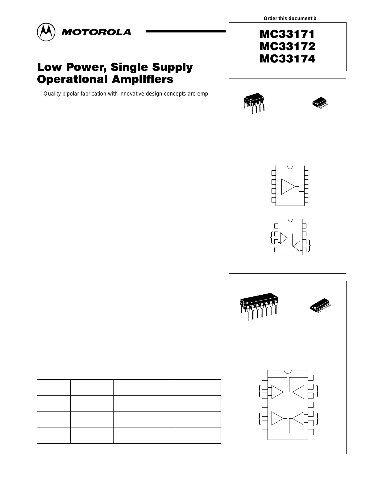
8
1
P SUFFIX
PLASTIC PACKAGE
CASE 626
PIN CONNECTIONS
Offset Null
Inv. Input
Noninv. Input
V
EE
Output 1 V
Inputs 1
V
EE
14
1
P SUFFIX
PLASTIC PACKAGE
CASE 646
DUAL
PLASTIC PACKAGE
1
2
–
+
3
4
(Single, Top View)
1
1
2
–
2
+
3
4
(Top View)
–
+
QUAD
PLASTIC PACKAGE
8
1
D SUFFIX
CASE 751
(SO–8)
8
NC
7
V
CC
Output
6
Offset Null
5
8
CC
7
Output 2
6
Inputs 2
5
14
1
D SUFFIX
CASE 751A
(SO–14)
ORDERING INFORMATION
Op Amp
Function
Single MC33171D
Dual MC33172D
Quad MC33174D
Device
MC33171P
MC33172P
MC33174P
Operating
Temperature Range
TA = –40° to +85°C
TA = –40° to +85°C
TA = –40° to +85°C
TA = –40° to +85°C
TA = –40° to +85°C
TA = –40° to +85°C
MOTOROLA ANALOG IC DEVICE DATA
Package
SO–8
Plastic DIP
SO–8
Plastic DIP
SO–14
Plastic DIP
PIN CONNECTIONS
Output 1
Inputs 1
Inputs 2
Output 2
Motorola, Inc. 1996 Rev 0
1
2
–
1
3
+
4
V
CC
5
+
23
–
6
78
(Top View)
14
Output 4
13
–
4
+
+
–
Inputs 4
12
11
V
EE
10
Inputs 3
9
Output 3
1
Page 2
MC33171 MC33172 MC33174
MAXIMUM RATINGS
Rating Symbol Value Unit
Supply Voltage VCC/V
Input Differential Voltage Range V
Input Voltage Range V
Output Short Circuit Duration (Note 2) t
Operating Ambient Temperature Range T
Operating Junction Temperature T
Storage Temperature Range T
NOTES: 1. Either or both input voltages must not exceed the magnitude of VCC or V
2.Power dissipation must be considered to ensure maximum junction temperature (TJ)
is not exceeded.
EE
IDR
IR
SC
A
J
stg
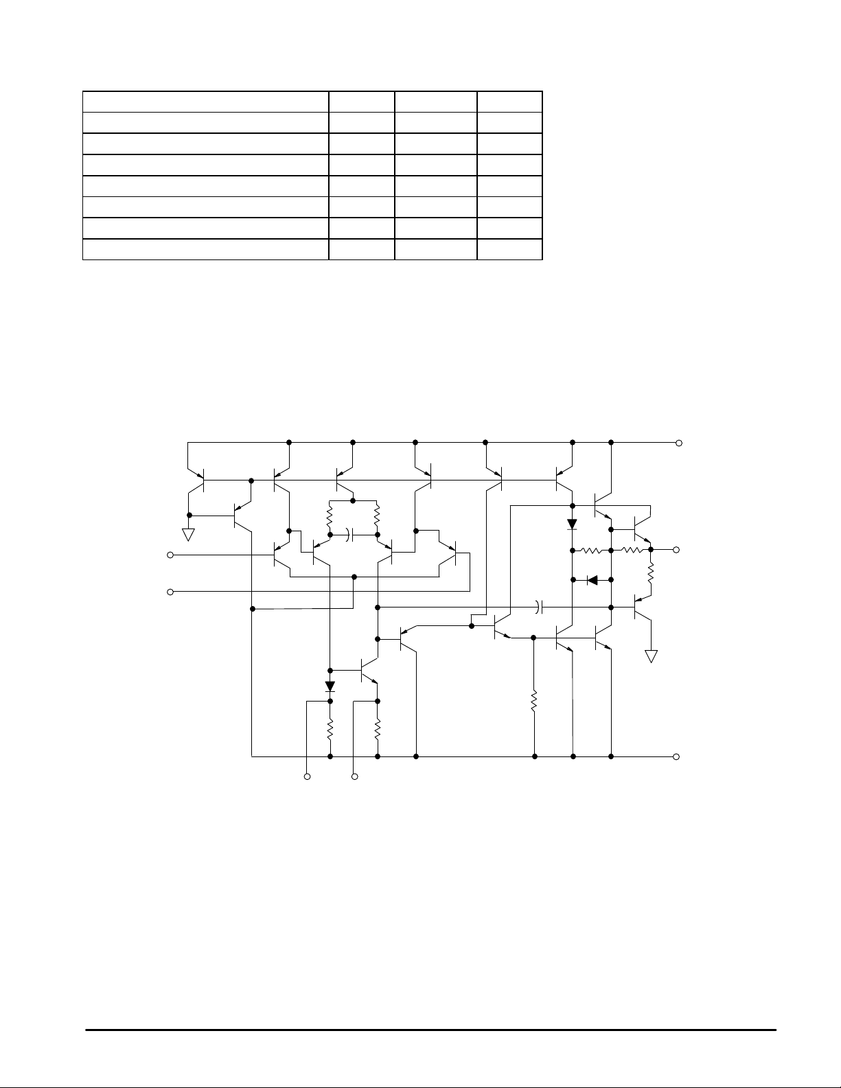
Representative Schematic Diagram
(Each Amplifier)
±22 V
(Note 1) V
(Note 1) V
Indefinite sec
–40 to +85 °C
+150 °C
–65 to +150 °C
EE.
–
Inputs
+
Q1
Bias
Q3 Q4 Q5 Q6 Q7
Q2
Q8
R1
C1
Q9 Q10
Q12
D1
R3 R4
Offset Null
(MC33171)
R2
Q11
Q13
Q14
Q17
D2
R6 R7
C2 D3
Q16Q15
R5
Q18
R8
Q19
Current
Limit
VEE/Gnd
V
CC
Output
2
MOTOROLA ANALOG IC DEVICE DATA
Page 3
MC33171 MC33172 MC33174
DC ELECTRICAL CHARACTERISTICS (V
unless otherwise noted.)
Characteristics
Input Offset Voltage (VCM = 0 V)
VCC = +15 V, VEE = –15 V, TA = +25°C
VCC = +5.0 V, VEE = 0 V, TA = +25°C
VCC = +15 V, VEE = –15 V, TA = T
Average Temperature Coefficient of Offset Voltage ∆VIO/∆T — 10 — µV/°C
Input Bias Current (VCM = 0 V)
TA = +25°C
TA = T
Input Offset Current (VCM = 0 V)
TA = +25°C
TA = T
Large Signal Voltage Gain (VO = ±10 V< RL = 10 k)
TA = +25°C
TA = T
Output Voltage Swing
VCC = +5.0 V, VEE = 0 V, RL = 10 k, TA = +25°C
VCC = +15 V, VEE = –15 V, RL = 10 k, TA = +25°C
VCC = +15 V, VEE = –15 V, RL = 10 k, TA = T
VCC = +5.0 V, VEE = 0 V, RL = 10 k, TA = +25°C
VCC = +15 V, VEE = –15 V, RL = 10 k, TA = +25°C
VCC = +15 V, VEE = –15 V, RL = 10 k, TA = T
Output Short Circuit (TA = +25°C)
Input Overdrive = 1.0 V , Output to Ground
Input Common Mode Voltage Range
TA = +25°C
TA = T
Common Mode Rejection Ratio (RS ≤ 10 k) TA = +25°C CMRR 80 90 — dB
Power Supply Rejection Ratio (RS = 100 Ω) TA = +25°C PSRR 80 100 — dB
Power Supply Current (Per Amplifier)
VCC = +5.0 V, VEE = 0 V, TA = +25°C
VCC = +15 V, VEE = –15 V, TA = +25°C
VCC = +15 V, VEE = –15 V, TA = T
NOTE: 3. T
low
low
low
Source
Sink
low
low
to T
high
to T
high
to T
high
to T
high
= –40°CT
high
= +85°C
low
low
to T
to T
= +15 V, VEE = –15 V, RL connected to ground, TA = T
CC
Symbol Min Typ Max Unit
V
IO
high
I
IB
I
IO
A
VOL
V
OH
to T
low
high
V
OL
to T
low
high
I
SC
V
ICR
I
D
high
to T
low
high
—
—
—
—
—
—
—
50
25
3.5
13.6
13.3
—
—
—
3.0
15
—
—
—
2.0
2.5
—
20
—
5.0
—
500
—
4.3
14.2
—
0.05
–14.2
—
5.0
27
VEE to (VCC –1.8)
VEE to (VCC –2.2)
180
220
—
[Note 3],
mV
4.5
5.0
6.5
100
200
20
40
V/mV
—
—
—
—
—
0.15
–13.6
–13.3
mA
—
—
250
250
300
nA
nA
V
V
µA
MOTOROLA ANALOG IC DEVICE DATA
3
Page 4
MC33171 MC33172 MC33174
AC ELECTRICAL CHARACTERISTICS (V
Characteristics Symbol Min Typ Max Unit
Slew Rate (Vin = –10 V to +10 V, RL = 10 k, CL = 100 pF)
AV +1
AV –1
Gain Bandwidth Product (f = 100 kHz) GBW 1.4 1.8 — MHz
Power Bandwidth
AV = +1.0 RL = 10 k, VO = 20 Vpp, THD = 5%
Phase Margin
RL = 10 k
RL = 10 k, CL = 100 pF
Gain Margin
RL = 10 k
RL = 10 k, CL = 100 pF
Equivalent Input Noise Voltage
RS = 100 Ω, f = 1.0 kHz
Equivalent Input Noise Current (f = 1.0 kHz) I
Differential Input Resistance
Vcm = 0 V
Input Capacitance C
Total Harmonic Distortion
AV = +10, RL = 10 k, 2.0 Vpp ≤ VO ≤ 20 Vpp, f = 10 kHz
Channel Separation (f = 10 kHz) CS — 120 — dB
Open Loop Output Impedance (f = 1.0 MHz) z
= +15 V, VEE = –15 V, RL connected to ground, TA = +25°C, unless otherwise noted.)
CC
SR
BWp — 35 — kHz
φ
m
A
m
e
n
n
R
in
i
THD — 0.03 — %
o
1.6
—
—
—
—
—
— 32 —
— 0.2 —
— 300 — MΩ
— 0.8 — pF
— 100 — Ω
2.1
2.1
60
45
15
5.0
—
—
—
—
—
—
V/µs
Degree
nV/ Hz√
pA/ Hz√
s
dB
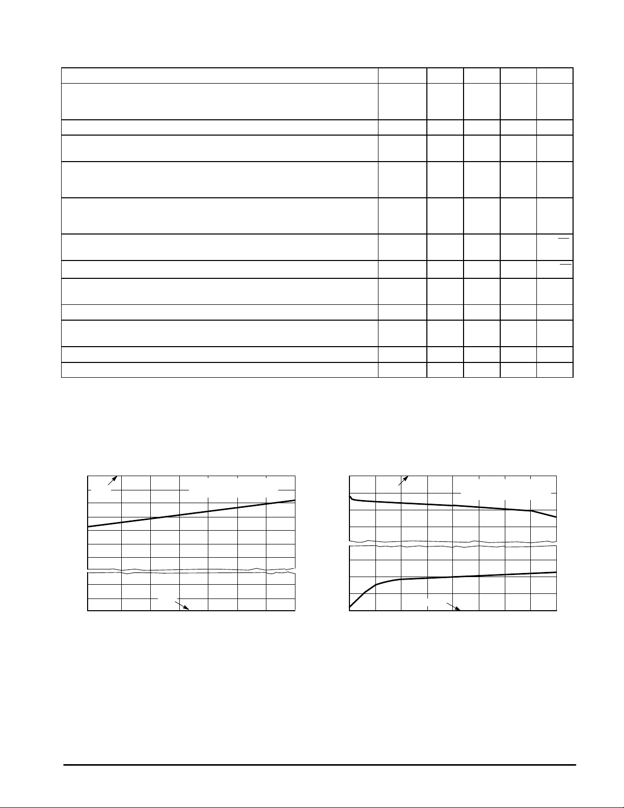
Figure 1. Input Common Mode V oltage Range
versus T emperature
0
V
CC
–0.8
–1.6
–2.4
0.1
V
0
–55 –25 0 25 50 75 100
ICR
V , INPUT COMMON MODE VOLTAGE RANGE (V)
TA, AMBIENT TEMPERATURE (°C)
VCC/VEE = ±1.5 V to ±22 V
∆
EE
VIO = 5.0 mV
Figure 2. Split Supply Output Saturation
versus Load Current
0
V
CC
–1.0
1.0
sat
V , OUTPUT SA TURATION VOLTAGE (V)
125 0 1.0 2.0 3.0 4.0
0
Source
Sink
V
IL, LOAD CURRENT (±mA)
VCC/VEE = ±5.0 V to ±22 V
EE
TA = 25
°
C
4
MOTOROLA ANALOG IC DEVICE DATA
Page 5

MC33171 MC33172 MC33174
Figure 3. Open Loop V oltage Gain and
Phase versus Frequency
3
0
20
10
VCC/VEE = ±15 V
0
RL = 10 k
V
= 0 V
out
–10
, OPEN LOOP VOL TAGE GAIN (dB)
–20
VOL
A
–30
100 k 1.0 M 10 M
°
C
TA = 25
1 — Phase
2 — Phase, CL = 100 pF
3 — Gain
4 — Gain, CL = 100 pF
f, FREQUENCY (Hz)
Phase
Margin
°
= 58
Margin
1
= 15 dB
2
4
3
Figure 5. Normalized Gain Bandwidth Product
and Slew Rate versus T emperature
1.3
1.2
GBW
1.1
1.0
0.9
VCC/VEE = ±15 V
RL = 10 k
SR
Gain
120
140
160
180
200
220
Figure 4. Phase Margin and Percent
Overshoot versus Load Capacitance
70
60
50
40
30
20
m, PHASE MARGIN (DEGREES)
, EXCESS PAHSE (DEGREES)
φ
10
φ
0
10 20 50 100 200 500 1.0 k
φ
Figure 6. Small and Large Signal
0
50 mV/DIV10 V/DIV
m
%
CL, LOAD CAPACITANCE (pF)
Transient Response
5.0 µs/DIV
VCC/VEE = ±15 V
VCM = 0 V
VO = 0 V
∆
IO = ±0.5 mA
°
C
TA = 25
VCC/VEE = ±15 V
A
= +1.0
VOL
RL = 10 k
∆
VO = 20 mV
TA = 25
pp
°
C
70
60
50
40
30
20
%, PERCENT OVERSHOOT
10
0
GBW AND SR (NORMALIZED)
0.8
0.7
–55 –25 0 25 50 75 100 125
TA, AMBIENT TEMPERATURE (
°
C)
0
5.0
µ
s/DIV
Figure 7. Output Impedance and Frequency Figure 8. Supply Current versus Supply V oltage
140
VCC/VEE = ±15 V
AV = +1.0
120
RL = 10 k
Ω
CL = 100 pF
100
80
60
40
o
z , OUTPUT IMPEDANCE ( )
20
0
200 2.0 k 20 k 200 k 2.0 M 0 5.0 10 15 20 25
TA = 25
°
C
AV = 1000
AV = 100
AV = 10 AV = 1.0
f, FREQUENCY (Hz)
1.1
0.9
0.7
0.5
0.3
CC
D
I , I , POWER SUPPLY CURRENT (mA)
0.1
1. TA = –55°C
2. TA = 25
3. TA = 125
°
°
C
C
VCC/VEE, SUPPLY VOLTAGE (±V)
Quad
Dual
Single
1
2
3
1
2
3
1
2
3
MOTOROLA ANALOG IC DEVICE DATA
5
Page 6

MC33171 MC33172 MC33174
APPLICATIONS INFORMATION – CIRCUIT DESCRIPTION/PERFORMANCE FEATURES
Although the bandwidth, slew rate, and settling time of the
MC33171/72/74 amplifier family is similar to low power op
amp products utilizing JFET input devices, these amplifiers
offer additional advantages as a result of the PNP transistor
differential inputs and an all NPN transistor output stage.
Because the input common mode voltage range of this
input stage includes the VEE potential, single supply
operation is feasible to as low as 3.0 V with the common
mode input voltage at ground potential.
The input stage also allows differential input voltages up to
±44 V, provided the maximum input voltage range is not
exceeded. Specifically, the input voltages must range
between VCC and VEE supply voltages as shown by the
maximum rating table. In practice, although
recommended,
voltage by approximately 3.0 V and decrease below the V
voltage by 0.3 V without causing product damage, although
output phase reversal may occur. It is also possible to source
up to 5.0 mA of current from VEE through either inputs’
clamping diode without damage or latching, but phase
reversal may again occur. If at least one input is within the
common mode input voltage range and the other input is
within the maximum input voltage range, no phase reversal
will occur. If both inputs exceed the upper common mode
input voltage limit, the output will be forced to its lowest
voltage state.
Since the input capacitance associated with the small
geometry input device is substantially lower (0.8 pF) than that
of a typical JFET (3.0 pF), the frequency response for a given
input source resistance is greatly enhanced. This becomes
evident in D–to–A current to voltage conversion applications
where the feedback resistance can form a pole with the input
capacitance of the op amp. This input pole creates a 2nd
Order system with the single pole op amp and is therefore
detrimental to its settling time. In this context, lower input
capacitance is desirable especially for higher values of
feedback resistances (lower current DACs). This input pole
can be compensated for by creating a feedback zero with a
capacitance across the feedback resistance, if necessary , to
reduce overshoot. For 10 kΩ of feedback resistance, the
MC33171/72/74 family can typically settle to within 1/2 LSB
of 8 bits in 4.2 µs, and within 1/2 LSB of 12 bits in 4.8 µs for
a 10 V step. In a standard inverting unity gain fast settling
configuration, the symmetrical slew rate is typically
± 2.1 V/µs. In the classic noninverting unity gain
configuration the typical output positive slew rate is also
2.1 V/µs, and the corresponding negative slew rate will
usually exceed the positive slew rate as a function of the fall
time of the input waveform.
The all NPN output stage, shown in its basic form on the
equivalent circuit schematic, offers unique advantages over
the more conventional NPN/PNP transistor Class AB output
stage. A 10 kΩ load resistance can typically swing within 0.8 V
of the positive rail (VCC) and negative rail (VEE), providing a
28.4 Vpp swing from ±15 V supplies. This large output swing
becomes most noticeable at lower supply voltages.
The positive swing is limited by the saturation voltage of
the current source transistor Q7, the VBE of the NPN pull–up
transistor Q17, and the voltage drop associated with the
short circuit resistance, R5. For sink currents less than
0.4 mA, the negative swing is limited by the saturation
voltage of the pull–down transistor Q15, and the voltage drop
across R4 and R5. For small valued sink currents, the above
voltage drops are negligible, allowing the negative swing
the input voltages can exceed the V
not
CC
EE
voltage to approach within millivolts of VEE. For sink currents
(> 0.4 mA), diode D3 clamps the voltage across R4. Thus the
negative swing is limited by the saturation voltage of Q15,
plus the forward diode drop of D3 (≈VEE +1.0 V). Therefore
an unprecedented peak–to–peak output voltage swing is
possible for a given supply voltage as indicated by the output
swing specifications.
If the load resistance is referenced to VCC instead of
ground for single supply applications, the maximum possible
output swing can be achieved for a given supply voltage. For
light load currents, the load resistance will pull the output to
VCC during the positive swing and the output will pull the load
resistance near ground during the negative swing. The load
resistance value should be much less than that of the
feedback resistance to maximize pull–up capability .
Because the PNP output emitter–follower transistor has
been eliminated, the MC33171/72/74 family offers a 15 mA
minimum current sink capability , typically to an output voltage
of (VEE +1.8 V). In single supply applications the output can
directly source or sink base current from a common emitter
NPN transistor for current switching applications.
In addition, the all NPN transistor output stage is inherently
faster than PNP types, contributing to the bipolar amplifier’s
improved gain bandwidth product. The associated high
frequency low output impedance (200 Ω typ @ 1.0 MHz)
allows capacitive drive capability from 0 pF to 400 pF without
oscillation in the noninverting unity gain configuration. The
60°C phase margin and 15 dB gain margin, as well as the
general gain and phase characteristics, are virtually
independent of the source/sink output swing conditions. This
allows easier system phase compensation, since output
swing will not be a phase consideration. The AC
characteristics of the MC33171/72/74 family also allow
excellent active filter capability, especially for low voltage
single supply applications.
Although the single supply specification is defined at 5.0 V ,
these amplifiers are functional to at least 3.0 V @ 25°C.
However slight changes in parametrics such as bandwidth,
slew rate, and DC gain may occur.
If power to this integrated circuit is applied in reverse
polarity, or if the IC is installed backwards in a socket, large
unlimited current surges will occur through the device that
may result in device destruction.
As usual with most high frequency amplifiers, proper lead
dress, component placement and PC board layout should
be exercised for optimum frequency performance. For
example, long unshielded input or output leads may result in
unwanted input/output coupling. In order to preserve the
relatively low input capacitance associated with these
amplifiers, resistors connected to the inputs should be
immediately adjacent to the input pin to minimize additional
stray input capacitance. This not only minimizes the input
pole for optimum frequency response, but also minimizes
extraneous “pick up” at this node. Supply decoupling with
adequate capacitance immediately adjacent to the supply pin
is also important, particularly over temperature, since many
types of decoupling capacitors exhibit great impedance
changes over temperature.
The output of any one amplifier is current limited and thus
protected from a direct short to ground. However, under such
conditions, it is important not to allow the device to exceed
the maximum junction temperature rating. Typically for ±15 V
supplies, any one output can be shorted continuously to
ground without exceeding the maximum temperature rating.
6
MOTOROLA ANALOG IC DEVICE DATA
Page 7

MC33171 MC33172 MC33174
Figure 9. AC Coupled Noninverting Amplifier
with Single +5.0 V Supply
2.2 k 510 k
C
V
in
in
1.0 k
100 k
AV = 101
BW ( –3.0 dB) = 20 kHz
+
–
100 k
V
CC
VO 0
C
O
V
O
RL
100 k
Figure 11. DC Coupled Inverting Amplifier
Maximum Output Swing with Single
+5.0 V Supply
100 k
4.7 k
100 k
+
–
1.0 M
50 k
R
L
V
CC
V
O
3.6 Vpp
Figure 10. AC Coupled Inverting Amplifier
with Single +5.0 V Supply
V
CC
100 k
100 k
10 k
C
in
V
in
AV = 10
BW ( –3.0 dB) = 200 kHz
+
–
10 k
VO 0
C
O
V
O
100 kRL
Figure 12. Offset Nulling Circuit
V
CC
7
3
+
2
6
5
–
1
4
10 k
3.8 Vpp
VO 2.5 V
V
in
AV = 10
BW ( –3.0 dB) = 200 kHz
Figure 13. Active High–Q Notch Filter
Vin
≥
0.2 Vdc
–
+
fo = 1.0 kHz
fo =
V
in
2C
0.02
R
0.01
2R
32 k
16 k16 k
R
C
2C
0.02
π
4
4.2 Vpp
V
1
RC
V
EE
Offset Nulling range is approximately ±80 mV with
a 10 k potentiometer, MC33171 only.
Figure 14. Active Bandpass Filter
V
CC
R3
2 H
π
fo = 30 kHz
Q = 10
HO = 1.0
O
Q
foC
V
O
R2 =
R1 R3
4Q2R1 –R3
Qo f
o
< 0.1
GBW
C
C
0.047
V
CC
R3
2.2 k
0.4
–
+
Then:
R1 =
R3 =
O
V
Given fo = center frequency
Ao = Gain at center frequency
Choose Value fo, Q, Ao, C
For less than 10% error for operational amplifier, where fo and GBW are expressed in Hz.
R1
1.1 k
in
0.047
R2
5.6 k
MOTOROLA ANALOG IC DEVICE DATA
7
Page 8

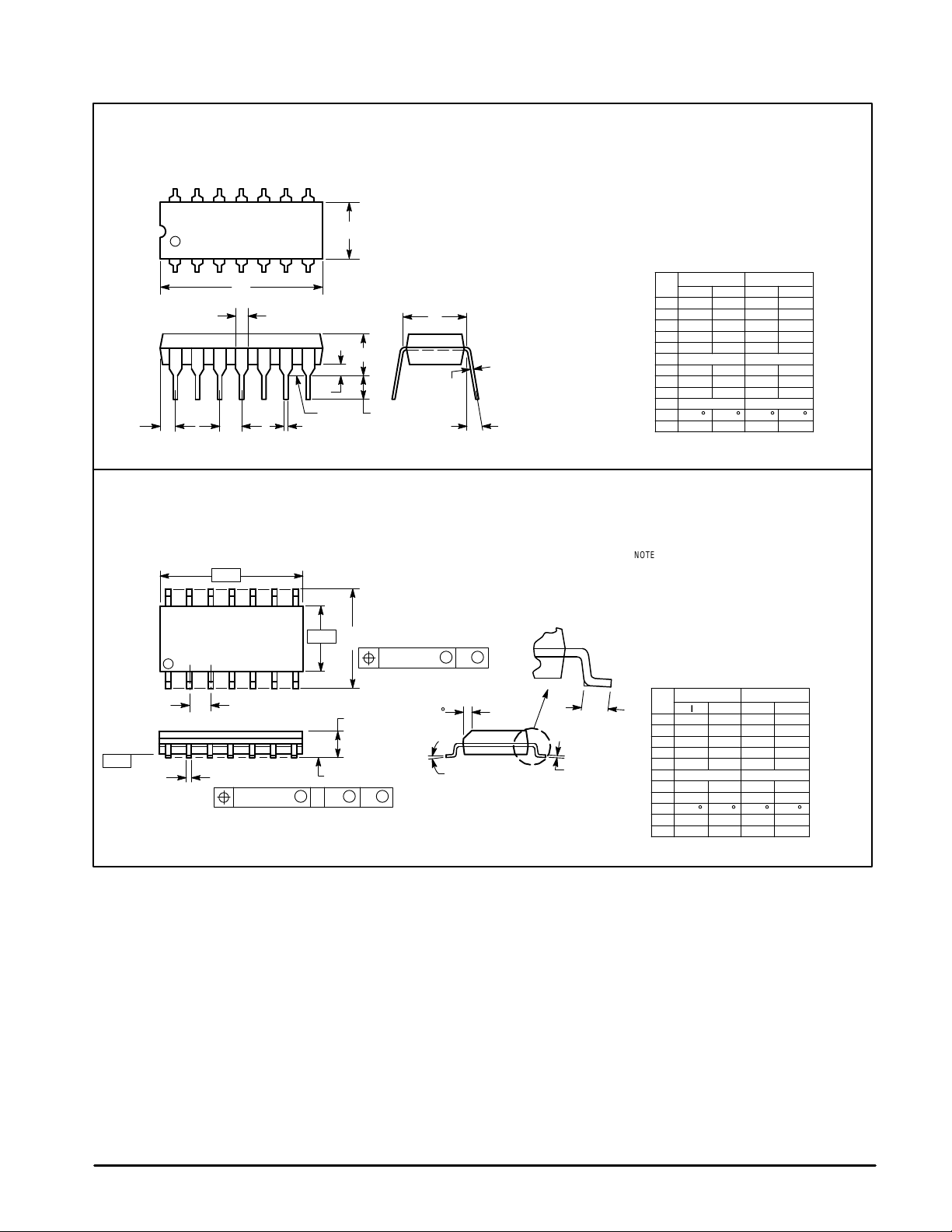
NOTE 2
–T–
SEATING
PLANE
H
MC33171 MC33172 MC33174
OUTLINE DIMENSIONS
58
–B–
14
F
–A–
C
N
D
G
0.13 (0.005) B
K
M
T
P SUFFIX
PLASTIC PACKAGE
CASE 626–05
ISSUE K
L
J
M
M
A
M
NOTES:
1. DIMENSION L TO CENTER OF LEAD WHEN
FORMED PARALLEL.
2. PACKAGE CONTOUR OPTIONAL (ROUND OR
SQUARE CORNERS).
3. DIMENSIONING AND TOLERANCING PER ANSI
Y14.5M, 1982.
DIM MIN MAX MIN MAX
A 9.40 10.16 0.370 0.400
B 6.10 6.60 0.240 0.260
C 3.94 4.45 0.155 0.175
D 0.38 0.51 0.015 0.020
F 1.02 1.78 0.040 0.070
G 2.54 BSC 0.100 BSC
H 0.76 1.27 0.030 0.050
J 0.20 0.30 0.008 0.012
K 2.92 3.43 0.115 0.135
L 7.62 BSC 0.300 BSC
M ––– 10 ––– 10
N 0.76 1.01 0.030 0.040
INCHESMILLIMETERS
__
D SUFFIX
PLASTIC PACKAGE
CASE 751–05
(SO–8)
ISSUE R
A
E
B
C
A1
D
58
0.25MB
1
H
4
e
M
h
X 45
_
q
C
A
SEATING
PLANE
0.10
L
B
SS
A0.25MCB
NOTES:
1. DIMENSIONING AND TOLERANCING PER ASME
Y14.5M, 1994.
2. DIMENSIONS ARE IN MILLIMETERS.
3. DIMENSION D AND E DO NOT INCLUDE MOLD
PROTRUSION.
4. MAXIMUM MOLD PROTRUSION 0.15 PER SIDE.
5. DIMENSION B DOES NOT INCLUDE MOLD
PROTRUSION. ALLOWABLE DAMBAR
PROTRUSION SHALL BE 0.127 TOTAL IN EXCESS
OF THE B DIMENSION AT MAXIMUM MATERIAL
CONDITION.
MILLIMETERS
DIM MIN MAX
A 1.35 1.75
A1 0.10 0.25
B 0.35 0.49
C 0.18 0.25
D 4.80 5.00
E
3.80 4.00
1.27 BSCe
H 5.80 6.20
h
0.25 0.50
L 0.40 1.25
0 7
q
__
8
MOTOROLA ANALOG IC DEVICE DATA
Page 9
–T–
SEATING
PLANE
MC33171 MC33172 MC33174
OUTLINE DIMENSIONS
P SUFFIX
PLASTIC PACKAGE
CASE 646–06
ISSUE L
14 8
B
17
A
F
N
SEATING
HG D
PLANE
–A–
14 8
–B–
P
71
G
C
D 14 PL
0.25 (0.010) A
K
M
S
B
T
C
K
7 PL
0.25 (0.010) B
S
L
J
M
D SUFFIX
PLASTIC PACKAGE
CASE 751A–03
(SO–14)
ISSUE F
M
X 45
R
_
M
NOTES:
1. LEADS WITHIN 0.13 (0.005) RADIUS OF TRUE
POSITION AT SEATING PLANE AT MAXIMUM
MATERIAL CONDITION.
2. DIMENSION L TO CENTER OF LEADS WHEN
FORMED PARALLEL.
3. DIMENSION B DOES NOT INCLUDE MOLD
FLASH.
4. ROUNDED CORNERS OPTIONAL.
DIM MIN MAX MIN MAX
A 0.715 0.770 18.16 19.56
B 0.240 0.260 6.10 6.60
C 0.145 0.185 3.69 4.69
D 0.015 0.021 0.38 0.53
F 0.040 0.070 1.02 1.78
G 0.100 BSC 2.54 BSC
H 0.052 0.095 1.32 2.41
J 0.008 0.015 0.20 0.38
K 0.115 0.135 2.92 3.43
L 0.300 BSC 7.62 BSC
M 0 10 0 10
____
N 0.015 0.039 0.39 1.01
NOTES:
1. DIMENSIONING AND TOLERANCING PER ANSI
Y14.5M, 1982.
2. CONTROLLING DIMENSION: MILLIMETER.
3. DIMENSIONS A AND B DO NOT INCLUDE
MOLD PROTRUSION.
4. MAXIMUM MOLD PROTRUSION 0.15 (0.006)
PER SIDE.
5. DIMENSION D DOES NOT INCLUDE DAMBAR
M
F
J
PROTRUSION. ALLOWABLE DAMBAR
PROTRUSION SHALL BE 0.127 (0.005) TOTAL
IN EXCESS OF THE D DIMENSION AT
MAXIMUM MATERIAL CONDITION.
DIM MIN MAX MIN MAX
A 8.55 8.75 0.337 0.344
B 3.80 4.00 0.150 0.157
C 1.35 1.75 0.054 0.068
D 0.35 0.49 0.014 0.019
F 0.40 1.25 0.016 0.049
G 1.27 BSC 0.050 BSC
J 0.19 0.25 0.008 0.009
K 0.10 0.25 0.004 0.009
M 0 7 0 7
____
P 5.80 6.20 0.228 0.244
R 0.25 0.50 0.010 0.019
MILLIMETERSINCHES
INCHESMILLIMETERS
MOTOROLA ANALOG IC DEVICE DATA
9
Page 10

MC33171 MC33172 MC33174
NOTES
10
MOTOROLA ANALOG IC DEVICE DATA
Page 11

MC33171 MC33172 MC33174
NOTES
MOTOROLA ANALOG IC DEVICE DATA
11
Page 12

MC33171 MC33172 MC33174
Motorola reserves the right to make changes without further notice to any products herein. Motorola makes no warranty , representation or guarantee regarding
the suitability of its products for any particular purpose, nor does Motorola assume any liability arising out of the application or use of any product or circuit, and
specifically disclaims any and all liability, including without limitation consequential or incidental damages. “T ypical” parameters which may be provided in Motorola
data sheets and/or specifications can and do vary in different applications and actual performance may vary over time. All operating parameters, including “Typicals”
must be validated for each customer application by customer’s technical experts. Motorola does not convey any license under its patent rights nor the rights of
others. Motorola products are not designed, intended, or authorized for use as components in systems intended for surgical implant into the body, or other
applications intended to support or sustain life, or for any other application in which the failure of the Motorola product could create a situation where personal injury
or death may occur. Should Buyer purchase or use Motorola products for any such unintended or unauthorized application, Buyer shall indemnify and hold Motorola
and its officers, employees, subsidiaries, affiliates, and distributors harmless against all claims, costs, damages, and expenses, and reasonable attorney fees
arising out of, directly or indirectly, any claim of personal injury or death associated with such unintended or unauthorized use, even if such claim alleges that
Motorola was negligent regarding the design or manufacture of the part. Motorola and are registered trademarks of Motorola, Inc. Motorola, Inc. is an Equal
Opportunity/Affirmative Action Employer.
How to reach us:
USA/EUROPE /Locations Not Listed: Motorola Literature Distribution; JAPAN: Nippon Motorola Ltd.; Tatsumi–SPD–JLDC, 6F Seibu–Butsuryu–Center,
P.O. Box 20912; Phoenix, Arizona 85036. 1–800–441–2447 or 602–303–5454 3–14–2 Tatsumi Koto–Ku, Tokyo 135, Japan. 03–81–3521–8315
MFAX: RMF AX0@email.sps.mot.com – TOUCHT ONE 602–244–6609 ASIA/PACIFIC: Motorola Semiconductors H.K. Ltd.; 8B Tai Ping Industrial Park,
INTERNET: http://Design–NET.com 51 Ting Kok Road, Tai Po, N.T., Hong Kong. 852–26629298
12
◊
MOTOROLA ANALOG IC DEVICE DATA
MC33171/D
*MC33171/D*
 Loading...