

Page 1
Device
Operating
Temperature Range
Package
SEMICONDUCTOR
TECHNICAL DATA
GaAs POWER AMPLIFIER
SUPPORT IC
ORDERING INFORMATION
MC33169DTB–4.0 TA = –40° to +85°C TSSOP–14
DTB SUFFIX
PLASTIC PACKAGE
CASE 948G
(TSSOP–14)
14
1
PIN CONNECTIONS
Order this document by MC33169/D
V
CC
Idle Mode Input
C2 Input
C1/C2
C1 Input
VO Output
VO Charge Pump
Capacitor+
Gnd
VO Charge Pump
Capacitor–
VBB Double
VBB Triple
Sense Input
Tx Power
Control Input
Gate Drive Output
(T op View)
1
2
3
4
5
6
7
14
13
12
11
10
9
8
1
MOTOROLA ANALOG IC DEVICE DATA
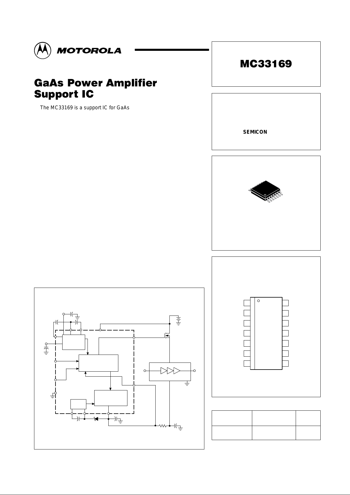
The MC33169 is a support IC for GaAs Power Amplifier Enhanced FETs
used in hand–held telephones such as GSM and PCS. This device provides
negative voltages for full depletion of Enhanced MESFETs as well as a
priority management system of drain switching, ensuring that the negative
voltage is always present before turning “on” the Power Amplifier. Additional
features include an idle mode input and a direct drive of the N–Channel drain
switch transistor. This product is available in a 4.0 V version intended for
control of the RF Power Amplifier in GSM, DCS1800 and PCS applications.
• Negative Regulated Output for Full Depletion of GaAs MESFETs
• Drain Switch Priority Management Circuit
• CMOS Compatible Inputs
• Idle Mode Input (Standby Mode) for Very Low Current Consumption
• Output Signal Directly Drives N–Channel FET
• Low Startup and Operating Current
Simplified Block Diagram
VBB Double
C3
V
CC
+–C1–+
C2
V
BB
Triple
C4
+
–
Tx Power
Control
Input
Idle
Mode Input
Gnd
C
p
+–
V
O
Output
(–4.0 V)
C
i
R
f
C
f
+–
+
RF
In
RF
Out
+
V
Battery
(2.7 to 7.0 V)
Gate Drive Output
Sense Input
V
BB
Generator
(Voltage Tripler)
Priority
Management
Negative
Generator
Charge
Pump
Power Amplifier
Sense
MC33169
MMSF4N01HD
21 14
8
10
457
6
13
9
3
11
+
12
This device contains 148 active transistors.
Motorola, Inc. 1998 Rev 2
Page 2
MC33169
2
MOTOROLA ANALOG IC DEVICE DATA
MAXIMUM RATINGS
Rating Pin Symbol Value Unit
Power Supply Voltage 14 V
CC
9.5 V
Tx Power Control Input 9 VT
x
V
CC
V
Idle Mode Input 13 V
i
V
CC
V
Sense Input 10 V
Sense
–5.0 to 0 V
Negative Generator Output Source Current 4 I
SS
20 mA
Charge Pump Capacitor Current – I
max
60 mA
Diode Forward Current – I
Fmax
60 mA
Gate Drive Output Current 8 I
GO
5.0 mA
Power Dissipation and Thermal Characteristics –
Maximum Power Dissipation @ TA = 50°C P
D
417 mW
Thermal Resistance, Junction–to–Air R
θJA
240 °C/W
Operating Junction Temperature T
J
+150 °C
Operating Ambient Temperature – T
A
–40 to +85 °C
Storage Temperature Range – T
stg
–60 to +150 °C
NOTE: ESD data available upon request.
MC33169–4.0
ELECTRICAL CHARACTERISTICS (V
CC
= 4.8 V . For typical values TA = 25°C, for min/max values TA is the operating
ambient temperature range that applies, unless otherwise noted.)
Characteristic
Pin Symbol Min Typ Max Unit
VBB GENERATOR (VOLTAGE TRIPLER)
Oscillator Frequency – f
osc
90 100 110 kHz
Oscillator Duty Cycle – DC 35 50 65 %
Output Voltage (VCC = 3.0 V , IO = 3.0 mA) Double Voltage 12 V
BBD
4.6 5.0 – V
Output Voltage (VCC = 3.0 V , IO = 3.0 mA) Triple V oltage 11 V
BBT
6.1 7.0 –
Output Voltage (VCC = 7.2 V , IO = 3.0 mA) Triple Voltage 11 V
BBT
– 11.2 –
NEGATIVE GENERATOR OUTPUT
Output Voltage (IO = 3.0 mA) 4 V
O
–3.75 –4.0 –4.25 V
Output Voltage Ripple with Filter (Rf = 33 Ω, Cf = 4.7 µF) 4 V
r
mVpp
(IO = 0 to 5.0 mA) – 2.0 –
PRIORITY MANAGEMENT SECTION
Idle Mode Input 13
Input Voltage High State (Logic 1) V
IH
2.0 – VCC+0.2 V
Input Voltage Low State (Logic 0) V
IL
0 – 0.5 V
Input Current High State (Logic 1) I
IH
10 – 80 µA
Input Current Low State (Logic 0), i.e. Standby Mode I
IL
– – 1.0 µA
Tx Power Control Input 9
Input Voltage Range VT
x
0 – 3.1 V
Input Voltage “Of f” State (Zero RF Output Level) VT
x(off)
– 0.7 – V
Input Voltage “On” State (Maximum RF Output Level) VT
x(on)
– 2.7 – V
Input Resistance R
in
– 90 – kΩ
Bandwidth (–3.0 dB) B – 1.0 – MHz
Gate Drive Output 8
Voltage (VTx = 0 V) V
GO
– – 0.5 V
Voltage (VTx = 3.0 V) VCC+2.7 – –
Peak Current (Source and Sink) (VTx = 3.0 V) I
GO
– 3.0 – mA
Undervoltage Lockout Voltage on Sense Input (Magnitude) 10 V
sense
–3.0 –3.2 – V
TOTAL DEVICE POWER CONSUMPTION
ICC Operating (VTx = 3.0 V , IO = 3.0 mA) – I
CC
– 10 15 mA
ICC Operating (VTx = 0 V, IO = 3.0 mA) – I
CC
– 12 15 mA
ICC Operating (VTx = 0 V, IO = 0 mA) – 4.0 5.0
Standby Mode (Idle Mode Input = 0 V) – I
CC
– – 1.0 µA
Page 3
MC33169
3
MOTOROLA ANALOG IC DEVICE DATA
MC33169–4.0
ELECTRICAL CHARACTERISTICS (V
CC
= 2.7 V . For typical values TA = 25°C, for min/max values TA is the operating
ambient temperature range that applies, unless otherwise noted.)
Characteristic
Pin Symbol Min Typ Max Unit
VBB GENERATOR (VOLTAGE TRIPLER)
Oscillator Frequency – f
osc
90 100 110 kHz
Oscillator Duty Cycle – DC 35 50 65 %
Output Voltage (VCC = 3.0 V , IO = 3.0 mA) V
Double Voltage 12 V
BBD
4.6 5.0 –
Triple V oltage 11 V
BBT
6.1 7.0 –
Triple V oltage (VCC = 7.2 V , IO = 3.0 mA) 11 V
BBT
– 11.2 –
NEGATIVE GENERATOR OUTPUT
Output Voltage (IO = 1.0 mA) 4 V
O
–3.75 –4.0 –4.25 V
Output Voltage Ripple with Filter (Rf = 33 Ω, Cf = 4.7 µF) 4 V
r
mVpp
(IO = 0 to 5.0 mA) – 2.0 –
PRIORITY MANAGEMENT SECTION
Idle Mode Input 13
Input Voltage High State (Logic 1) V
IH
2.0 – VCC+0.2 V
Input Voltage Low State (Logic 0) V
IL
0 – 0.5 V
Input Current High State (Logic 1) I
IH
10 – 80 µA
Input Current Low State (Logic 0), i.e. Standby Mode I
IL
– – 1.0 µA
Tx Power Control Input 9
Input Voltage Range VT
x
0 – 3.0 V
Input Voltage “Of f” State (Zero RF Output Level) VT
x(off)
– 0.7 – V
Input Voltage “On” State (Maximum RF Output Level) VT
x(on)
– 2.7 – V
Input Resistance R
in
– 90 – kΩ
Bandwidth (–3.0 dB) B – 1.0 – MHz
Gate Drive Output 8
Voltage (VTx = 0 V) V
GO
– – 0.5 V
Voltage (VTx = 3.0 V) VCC+2.7 – –
Peak Current (Source and Sink) (VTx = 3.0 V) I
GO
– 3.0 – mA
Undervoltage Lockout Voltage on Sense Input (Magnitude) 10 V
sense
–3.0 –3.2 – V
TOTAL DEVICE POWER CONSUMPTION
ICC Operating (VTx = 3.0 V) 14 I
CC
mA
(IO = 3.0 mA) – – 15
(IO = 1.0 mA) – – 9.0
ICC Operating (VTx = 0 V) 14 I
CC
mA
(IO = 3.0 mA) – – 13
(IO = 1.0 mA) – – 9.0
(IO = 0 mA) – 4.5 6.0
Standby Mode (Idle Mode Input = 0 V) 14 I
CC
– – 1.0 µA
PRIORITY MANAGEMENT TRUTH TABLE
Control Inputs Outputs
Idle Mode Tx Power Control V
O
Gate Drive
0
1
0
1
0
0
1
1
Off
–4.0 V
Off
–4.0 V
0.5 V max
0.5 V max
0.5 V max
VCC + 2.7 V min
Page 4

MC33169
4
MOTOROLA ANALOG IC DEVICE DATA
PIN FUNCTION DESCRIPTION
Pin Name Description
1 C2 Input This is the positive pin for the charge pump capacitor in the voltage doubler.
2 C1/C2 This is the negative pin for the charge pump capacitors.
3 C1 Input This is the positive pin for the charge pump capacitor in the voltage tripler.
4 VO Output It delivers a regulated negative voltage of –4.0 V . It can source an output current in excess of 5.0 mA.
5 VO Charge Pump
Capacitor +
This is the positive pin for the capacitor in the inverting charge pump.
6 Gnd This pin is Ground for both signal and power circuitry.
7 VO Charge Pump
Capacitor –
This is the negative pin for the capacitor in the inverting charge pump.
8 Gate Drive Output This is the output of the gate amplifier which directly drives the gate of an N–Channel MOSFET. It can
sink and source peak currents up to 3.0 mA.
9 Tx Power Control
Input
The input signal applied on this pin controls the N–Channel switching MOSFET in follower mode and
therefore, linearly controls the RF output voltage.
10 Sense Input Pin It senses the negative voltage directly on the Power Amplifier. It is also the input pin of an internal
Undervoltage Lockout circuit which blocks the switching of the N–Channel MOSFET if the sensed
voltage is more positive than –3.0 V .
11 VBB Triple This is the positive pin of the output filter capacitor in the voltage tripler. The triple voltage at that pin is
used internally to supply the inverting charge pump and the gate amplifier.
12 VBB Double This is the positive pin of the output filter capacitor in the voltage doubler.
13 Idle Mode Input This pin is used to set the circuit in Low Power Consumption Standby mode. It is CMOS compatible, i.e.
a voltage lower than 0.5 V applied on this pin makes the device go into Standby mode in which the
current consumption is lower than 1.0 µA. The MC33169 is then awakened by a voltage higher than
2.0 V applied on that pin.
14 V
CC
This is the supply input pin for the MC33169, VCC voltage ranges from 2.7 V to 7.2 V .
Figure 1. MC33169 Representative Block Diagram
123
C2 C1
VBB Double
12
C
d
9
T
x(on)
GaAs
PA
RF OutRF In
10 V
sense
4576 Gnd
C
p
C
n
V
O
Negative
Charge Pump
Negative Regulator
(–4.0)
Gate
Amplifier
Oscillator
Positive
Charge Pump
Positive
Regulator
14
V
CC
VBB Triple
11
13
Idle Mode
Input
C
t
+V
Battery
V
Gout
8
V
DD
UVLO
Voltage
Reference
Standby
Circuit
Priority
Management
Page 5

MC33169
5
MOTOROLA ANALOG IC DEVICE DATA
Figure 2. Operating Current versus Temperature Figure 3. Operating Current versus Temperature
Figure 4. Operating Current versus Temperature Figure 5. Operating Current versus Temperature
Figure 6. Output Voltage versus Temperature Figure 7. Output Voltage versus Temperature
TA, AMBIENT TEMPERATURE (°C)TA, AMBIENT TEMPERATURE (°C)
–50
TA, AMBIENT TEMPERATURE (
°
C)
TA, AMBIENT TEMPERATURE (
°
C)
TA, AMBIENT TEMPERATURE (
°
C)
TA, AMBIENT TEMPERATURE (
°
C)
V
SS
, OUTPUT VOL TAGE (V) I
CC
, OPERATING (mA)
I
CC
, OPERATING (mA)
I
CC
, OPERATING (mA)
I
CC
, OPERATING (mA)
OUTPUT VOLTAGE (V)
5.0
4.5
4.0
3.5
3.0
2.5
–25 0 25 50 75 100
VCC = 4.8 V
VCC = 2.7 V
15
–50 –25 0 25 50 75 100
VTx = 0 V
IO = 0 mA
VTx = 0 V
IO = 0 mA
15
14
13
12
16
–50 –25 0 25 50 75 100
VCC = 4.8 V
VTx = 3.0 V
IO = 3.0 mA
VTx = 3.0 V
VTx = 0 V
VCC = 2.7 V
IO = 1.0 mA
8.0
7.6
7.2
6.8
6.4
6.0
–50 –25 0 25 50 75 100
–4.03
–4.025
–4.02
–4.015
–4.01
–4.005
–4.0
–4.035
–4.04
–50 –25 0 25 50 75 100
ISS = 1.0 mA
VCC = 2.7 V
–4.0
–3.98
–3.96
–3.94
–4.04
–50 –25 0 25 50 75 100
–4.02
VCC = 4.8 V
VCC = 2.7 V
VCC = 4.8 V
VCC = 2.7 V
ISS = 3.0 mA
ISS = 3.0 mA
14
13
12
11
10
Page 6

MC33169
6
MOTOROLA ANALOG IC DEVICE DATA
Figure 8. Output Voltage versus Load Current
Figure 9. VTx Control Voltage versus Gate
Drive Output Voltage
VTx, POWER CONTROL INPUT VOLTAGE (V)
–4.03
–4.025
–4.02
–4.015
–4.01
–4.035
–4.04
0
V
GO
, GATE DRIVE OUTPUT VOLTAGE (V)
OUTPUT VOLTAGE (V)
0.5 1.0 1.5 2.0 2.5 3.0 3.5 4.0
8.0
7.0
6.0
5.0
4.0
3.0
2.0
1.0
0
0 0.5 1.0 1.5 2.0 2.5 3.0
85°C
25°C
–25°C
0°C
LOAD CURRENT (mA)
OPERA TING DESCRIPTION
The MC33169 is a power amplifier support IC that is
designed to properly switch “on” or “off” a MESFET Power
Amplifier either manually or by microprocessor. Controlling
the power drain of the RF Amplifier extends operating battery
life in many portable systems.
Outputs
The IC is designed to provide a –4.0 V bias to the gate of
the RF Ampllifier MESFET devices prior to application of a
positive battery voltage to the drain. The negative output
voltage can provide up to 5.0 mA of current. The positive
voltage control requires an external N–Channel logic level
MOSFET, connected as a source follower. The Gate Drive
Output, Pin 8, can source or sink 3.0 mA to the external
MOSFET. The low drive current slows the MOSFET
switching speed, thereby minimizing voltage glitches on the
VCC line which could cause disturbances to other circuitry.
Inputs
A Sense Input, Pin 10, protects the Power Amplifier load
by monitoring the level of the negative output voltage. If the
negative voltage magnitude falls below a preset level, 3.2 V
typical, an undervoltage lockout circuit disables the external
MOSFET gate drive.
The Tx Power Control Input controls the N–Channel
external switching MOSFET in source follower mode, which
allows linear control of the RF Output voltage level.
The Idle mode input is CMOS compatible, allowing the RF
Amplifier to be placed in a standby mode, drawing less than
1.0 µA from the power source.
Page 7

MC33169
7
MOTOROLA ANALOG IC DEVICE DATA
MRF IC 093
MC33169
Figure 10. Class 4 GSM with a Two–Stage Integrated Power Amplifier (I.P.A.)
C2 0.1
C1 0.1
Cp 1.0
MMBD701
LT1
14
13
12
11
10
9
8
1
2
3
4
5
6
7
5
6
7
8
4
3
2
1
8
7
6
5
4
3
2
1
9
10
11
12
13
14
15
16
3.0 V
0V
Idle
V
Batt
= 4.8 V
(4 cells
NlCd/NIMH)
Tx Power
Control
Input
3.0 V
0V
C3 1.0
C4 1.0
MMSF4N01HD
Drain
G
S
.047 47 pF
VG2 tune
VG1 tune
8.2 nH
50
Ω
In
6.8 pF
3.3 k
1.0 k
In
Out
Out
Grounded Backside
R
F
330
5.6 pF 5.6 pF
47 pF
50
Ω
Out
4 mm2 mm
47 pF .047
–4.0 V
30
Ω
30
Ω
Ci 0.22
100
100
S
C
f
0.22
68
Figure 11. Transfer Characteristic for
Gate Drive Output
VTx (V)
1.4
0 0.5 1.0 1.5 2.0 2.5
1.2
1.0
0.8
0.6
0.4
0.2
0
IPA RF
OUT
(Vrms)
TA = 25°C
V
Batt
= 4.8 V
V
Idle
= 3.0 V
V
Batt
= 4.8 V
Pin = 10 dBm
V
Idle
= 3.0 V
V
ramp
: 40 Hz sinusoidal voltage
set for 95% AM depth on RF
Peak output
power: 34.6 dBm
Page 8

MC33169
8
MOTOROLA ANALOG IC DEVICE DATA
CURVES RELATED TO APPLICATION GSM CLASS 4
Output RF
Voltage
Figure 12. RF Output Voltage (40 Hz/95% AM) and
VTx Driving Voltage
Figure 13. Idle, PA Drain, RF Output and V
O
Voltages During a Burst Period
VT
x
AND RF OUTPUT (V)
–50 ms –25 ms 0 s
TIMEBASE = 5.0 ms/DIV
VERTICAL SCALE = 0.5 V/DIV
V
T
VT
x
–0 V
0 V
0 V
–350 µs 150 µs 850 µs
TIMEBASE = 5.0
µ
s/DIV
VERTICAL SCALE = 0.5 V/DIV
V
O
0 V
Idle Voltage
VT
x
Output RF Voltage
Negative
Voltage
Figure 14. RF Output Voltage, PA Drain Voltage
and VTx Driving Voltage, During Fall Time
Figure 15. RF Output Voltage, PA Drain Voltage and
VTx Driving Voltage, During Rise Time
–13.4 µs 11.6 µs 36.6 µs
TIMEBASE = 5.0
µ
s/DIV
VERTICAL SCALE = 0.5 V/DIV
–13.4
µ
s 11.6 µs 36.6 µs
VERTICAL SCALE = 0.5 V/DIV
VT
x
PA Drain
Voltage
Output
RF Voltage
VT
x
PA Drain
Voltage
Output
RF Voltage
Page 9

MC33169
9
MOTOROLA ANALOG IC DEVICE DATA
MC33169
Figure 16. AMPS version with MRFIC0913, Integrated Power Amplifier (I.P.A.)
C2 0.1
C1 0.1
Cp 1.0
MMBD701
LT1
14
13
12
11
10
9
8
1
2
3
4
5
6
7
5
6
7
8
4
3
2
1
8
7
6
5
4
3
2
1
9
10
11
12
13
14
15
16
3.0 V
0V
Idle
V
Batt
= 3.6 V
(3 cells
NlCd/NIMH)
Tx Power
Control
Input
3.0 V
0V
C3 1.0
C4 1.0
MMSF4N01HD
Drain
G
S
.047 68 pF
VG2 tune
VG1 tune
10 nH
50
Ω
In
6.8 pF
3.3 k
1.0 k
In
Out
Out
Grounded Backside
R
f
330
5.6 pF 5.6 pF
68 pF
50
Ω
Out
7 mm2.5 mm
68 pF .047
–4.0 V
30
Ω
30
Ω
Ci 0.22
100
100
MRFIC0913
S
C
f
0.22
68
Figure 17. MC33169 with GaAs RF Power Amplifier
MC33169
C2 0.1
C1 0.1
Cp 1.0
MMBD701
LT1
14
13
12
11
10
9
8
1
2
3
4
5
6
7
5
6
7
8
4
3
2
1
3.0 V
0V
Idle
Tx Power
Control
Input
V
Batt
3.0 V
0V
C3 1.0
C4 1.0
MMSF4N01HD
Drain
G
S
R
f
330
C
f
0.22
–4.0 V
RF In RF Out
V
DD
V
O
GaAs Power Amplifier
50 Ω In 50 Ω Out
Ci 0.22
100
100
S
68
Page 10

MC33169
10
MOTOROLA ANALOG IC DEVICE DATA
DTB SUFFIX
PLASTIC PACKAGE
CASE 948G–01
(TSSOP–14)
ISSUE O
OUTLINE DIMENSIONS
DIM MIN MAX MIN MAX
INCHESMILLIMETERS
A 4.90 5.10 0.193 0.200
B 4.30 4.50 0.169 0.177
C ––– 1.20 ––– 0.047
D 0.05 0.15 0.002 0.006
F 0.50 0.75 0.020 0.030
G 0.65 BSC 0.026 BSC
H 0.50 0.60 0.020 0.024
J 0.09 0.20 0.004 0.008
J1 0.09 0.16 0.004 0.006
K 0.19 0.30 0.007 0.012
K1 0.19 0.25 0.007 0.010
L 6.40 BSC 0.252 BSC
M 0 8 0 8
NOTES:
1 DIMENSIONING AND TOLERANCING PER ANSI
Y14.5M, 1982.
2 CONTROLLING DIMENSION: MILLIMETER.
3 DIMENSION A DOES NOT INCLUDE MOLD FLASH,
PROTRUSIONS OR GATE BURRS. MOLD FLASH
OR GATE BURRS SHALL NOT EXCEED 0.15
(0.006) PER SIDE.
4 DIMENSION B DOES NOT INCLUDE INTERLEAD
FLASH OR PROTRUSION. INTERLEAD FLASH OR
PROTRUSION SHALL NOT EXCEED
0.25 (0.010) PER SIDE.
5 DIMENSION K DOES NOT INCLUDE DAMBAR
PROTRUSION. ALLOWABLE DAMBAR
PROTRUSION SHALL BE 0.08 (0.003) TOTAL IN
EXCESS OF THE K DIMENSION AT MAXIMUM
MATERIAL CONDITION.
6 TERMINAL NUMBERS ARE SHOWN FOR
REFERENCE ONLY.
7 DIMENSION A AND B ARE TO BE DETERMINED
AT DATUM PLANE –W–.
____
S
U0.15 (0.006) T
2X L/2
S
U
M
0.10 (0.004) V
S
T
L
–U–
SEATING
PLANE
0.10 (0.004)
–T–
SECTION N–N
DETAIL E
J
J1
K
K1
DETAIL E
F
M
–W–
0.25 (0.010)
8
14
7
1
PIN 1
IDENT.
H
G
A
D
C
B
S
U0.15 (0.006) T
–V–
14X REFK
N
N
Motorola reserves the right to make changes without further notice to any products herein. Motorola makes no warranty , representation or guarantee regarding
the suitability of its products for any particular purpose, nor does Motorola assume any liability arising out of the application or use of any product or circuit, and
specifically disclaims any and all liability, including without limitation consequential or incidental damages. “T ypical” parameters which may be provided in Motorola
data sheets and/or specifications can and do vary in different applications and actual performance may vary over time. All operating parameters, including “Typicals”
must be validated for each customer application by customer’s technical experts. Motorola does not convey any license under its patent rights nor the rights of
others. Motorola products are not designed, intended, or authorized for use as components in systems intended for surgical implant into the body, or other
applications intended to support or sustain life, or for any other application in which the failure of the Motorola product could create a situation where personal injury
or death may occur. Should Buyer purchase or use Motorola products for any such unintended or unauthorized application, Buyer shall indemnify and hold Motorola
and its officers, employees, subsidiaries, affiliates, and distributors harmless against all claims, costs, damages, and expenses, and reasonable attorney fees
arising out of, directly or indirectly, any claim of personal injury or death associated with such unintended or unauthorized use, even if such claim alleges that
Motorola was negligent regarding the design or manufacture of the part. Motorola and are registered trademarks of Motorola, Inc. Motorola, Inc. is an Equal
Opportunity/Affirmative Action Employer.
Mfax is a trademark of Motorola, Inc.
How to reach us:
USA/EUROPE/Locations Not Listed: Motorola Literature Distribution; JAPAN: Motorola Japan Ltd.; SPD, Strategic Planning Office, 141,
P.O. Box 5405, Denver, Colorado 80217. 1–303–675–2140 or 1–800–441–2447 4–32–1 Nishi–Gotanda, Shinagawa–ku, Tokyo, Japan. 81–3–5487–8488
Customer Focus Center: 1–800–521–6274
Mfax: RMFAX0@email.sps.mot.com – TOUCHTONE 1–602–244–6609 ASIA/PACIFIC: Motorola Semiconductors H.K. Ltd.; 8B Tai Ping Industrial Park,
Moto rola Fax Back Sys tem – US & Canada ONLY 1–800–774–1848 51 Ting Kok Road, Tai Po, N.T., Hong Kong. 852–26629298
– http://sps.motorola.com/mfax/
HOME PAGE: http://motorola.com/sps/
MC33169/D
◊
 Loading...