

Datasheet MC34160DW, MC34160DWR2, MC34160P, MC33160DW, MC33160DWR2 Datasheet (Motorola)
...Page 1
Order this document by MC34160/D
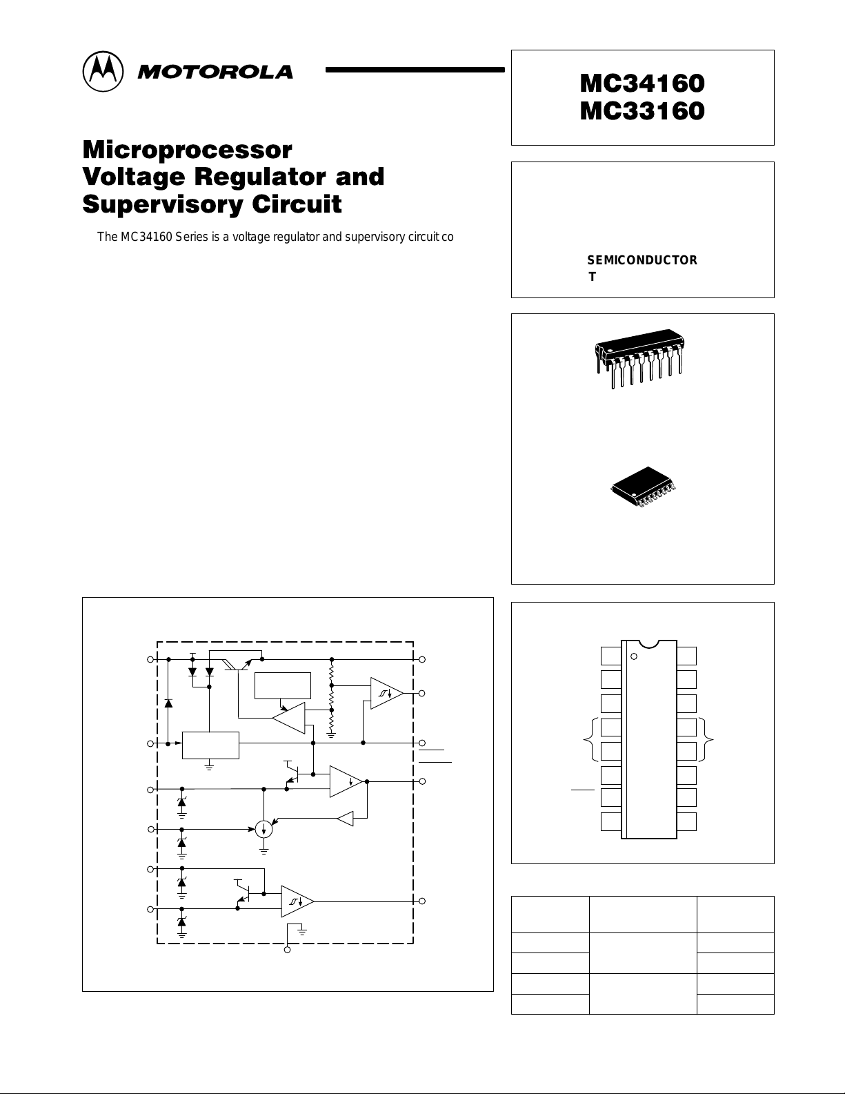
The MC34160 Series is a voltage regulator and supervisory circuit containing
many of the necessary monitoring functions required in microproces sor based
systems. It is specifically designed for appliance and industrial applications,
offering the designer a cost effective solution with minimal external components.
These integrated circuits feature a 5.0 V/100 mA regulator with short circuit
current limiting, pinned out 2.6 V bandgap reference, low voltage reset
comparator, power warning comparator with programmable hysteresis, and an
uncommitted comparator ideally suited for microprocessor line synchronization.
Additional features include a chip disable input for low standby current,
and internal thermal shutdown for over temperature protection.
These devices are contained in a 16 pin dual–in–line heat tab plastic
package for improved thermal conduction.
• 5.0 V Regulator Output Current in Excess of 100 mA
• Internal Short Circuit Current Limiting
• Pinned Out 2.6 V Reference
• Low Voltage Reset Comparator
• Power Warning Comparator with Programmable Hysteresis
• Uncommitted Comparator
• Low Standby Current
• Internal Thermal Shutdown Protection
• Heat Tab Power Package
MICROPROCESSOR
VOLTAGE REGULATOR/
SUPERVISORY CIRCUIT
SEMICONDUCTOR
TECHNICAL DATA
16
1
P SUFFIX
PLASTIC PACKAGE
CASE 648C
(DIP–16)
16
1
DW SUFFIX
PLASTIC PACKAGE
CASE 751G
(SOP–16L)
V
CC
14
Chip Disable
15
Power
Sense
9
Hysteresis
Adjust
10
Noninverting
Input
2
Inverting
Input
1
Representative Block Diagram
+
Thermal
Shutdown
2.6 V
Reference
+
This device contains 72 active transistors.
+
I
H
IH On/Off
+
–
Gnd 4, 5, 12, 13
0.913 R
+
0.01 R
–
+
–
+
–
R
Regulator
Output
11
Reset
7
Reference
Output
16
Power
Warning
8
Comparator
Output
6
PIN CONNECTIONS
1
Comp. Noninv. In
Gnd
Comp. Out
Power Warning Power Sense
2
3
N.C.
4
5
6
7
Reset
89
(Top View)
16Comp. Inv. In
V
ref
15
Chip Disable
14
V
CC
13
12
11
Reg. Out
10
Hyst. Adj.
ORDERING INFORMATION
Operating
Device
MC34160DW
MC34160P
MC33160DW
MC33160P
Temperature Range
TA = 0° to +70°C
TA = – 40° to +85°C
Package
SOP–16L
DIP–16
SOP–16L
DIP–16
Gnd
MOTOROLA ANALOG IC DEVICE DATA
Motorola, Inc. 1996 Rev 1
1
Page 2
MC34160 MC33160
MAXIMUM RATINGS
Rating Symbol Value Unit
Power Supply Voltage V
Chip Disable Input Voltage (Pin 15, Note 1) V
Comparator Input Current (Pins 1, 2, 9) I
Comparator Output Voltage (Pins 6, 7, 8) V
Comparator Output Sink Current (Pins 6, 7, 8) I
Power Dissipation and Thermal Characteristics
P Suffix, Dual–In–Line Case 648C
Thermal Resistance, Junction–to–Air
Thermal Resistance, Junction–to–Case (Pins 4, 5, 12, 13)
DW Suffix, Surface Mount Case 751G
Thermal Resistance, Junction–to–Air
Thermal Resistance, Junction–to–Case (Pins 4, 5, 12, 13)
Operating Junction Temperature T
Operating Ambient Temperature
MC34160
MC33160
Storage Temperature Range T
Sink
R
R
R
R
CC
–0.3 to V
CD
–2.0 to +2.0 mA
in
O
θJA
θJC
θJA
θJC
J
T
A
–40 to +85
–65 to +150 °C
stg
40 V
CC
40 V
10 mA
80
15
94
18
+150 °C
0 to +70
V
°C/W
°C
ELECTRICAL CHARACTERISTICS (V
operating ambient temperature range that applies [Notes 2 and 3], unless otherwise noted.)
Characteristics
REGULATOR SECTION
Total Output Variation (VCC = 7.0 V to 40 V,
IO = 1.0 mA to 100 mA, TA = T
Line Regulation (VCC = 7.0 V to 40 V, TA = 25°C) Reg
Load Regulation (IO = 1.0 V to 100 mA, TA = 25°C) Reg
Ripple Rejection
(VCC = 25 V to 35 V, IO = 40 mA, f = 120 Hz, TA = 25°C)
REFERENCE SECTION
Total Output Variation (VCC = 7.0 to 40 V,
IO = 0.1 mA to 2.0 mA, TA = T
Line Regulation (VCC = 5.0 V to 40 V, TA = 25°C) Reg
Load Regulation (IO = 0.1 mA to 2.0 mA, TA = 25°C) Reg
RESET COMPARATOR
Threshold Voltage
High State Output (Pin 11 Increasing)
Low State Output (Pin 11 Decreasing)
Hysteresis
Output Sink Saturation (VCC = 4.5 V, I
Output Off–State Leakage (VOH = 40 V) I
NOTES: 1. The maximum voltage range is –0.3 V to VCC or +35 V, whichever is less.
2.T
=0°C for MC34160 T
low
3.Low duty cycle pulse testing techniques are used during test to maintain junction temperature as close to ambient as possible.
–40°C for MC33160 85°C for MC33160
low
low
to T
to T
= 30 V , IO = 10 mA, I
CC
high)
high)
= 2.0 mA) V
Sink
=70°C for MC34160
high
= 100 µA) For typical values TA = 25°C, for min/max values TA is the
ref
Symbol Min Typ Max Unit
V
O
line
load
RR 50 6.5 – dB
V
ref
line
load
V
IH
V
IL
V
H
OL
OH
4.75 5.0 5.25 V
– 5.0 40 mV
– 20 50 mV
2.47 2.6 2.73 V
– 2.0 20 mV
– 4.0 30 mV
–
4.55
0.02
– – 0.4 V
– – 4.0 µA
(VO–0.11)
(VO–0.18)
0.07
(VO–0.05)
V
–
–
2
MOTOROLA ANALOG IC DEVICE DATA
Page 3
MC34160 MC33160
ELECTRICAL CHARACTERISTICS (continued) (V
values TA is the operating ambient temperature range that applies [Notes 2 and 3], unless otherwise noted.)
Characteristics Symbol Min Typ Max Unit
POWER WARNING COMPARATOR
Input Offset Voltage V
Input Bias Current (V
Input Hysteresis Current (V
R
= 24 k
Pin 10
R
= ∞
Pin 10
Output Sink Saturation (I
Output Off–State Leakage (VOH = 40 V) I
UNCOMMITTED COMPARATOR
Input Offset Voltage (Output Transition Low to High) V
Input Hysteresis Voltage (Output Transition High to Low) I
Input Bias Current (V
Input Common Mode Voltage Range V
Output Sink Saturation (I
Output Off–State Leakage (VOH = 40 V) I
TOTAL DEVICE
Chip Disable Threshold Voltage (Pin 15)
High State (Chip Disabled)
Low State (Chip Enabled)
Chip Disable Input Current (Pin 15)
High State (Vin = 2.5 V)
Low State (Vin = 0.8 V)
Chip Disable Input Resistance (Pin 15) R
Operating Voltage Range
VO (Pin 11) Regulated
V
(Pin 16) Regulated
ref
Power Supply Current
Standby (Chip Disable High State)
Operating (Chip Disable Low State)
NOTES: 1. The maximum voltage range is –0.3 V to VCC or +35 V, whichever is less.
2.T
=0°C for MC34160 T
low
3.Low duty cycle pulse testing techniques are used during test to maintain junction temperature as close to ambient as possible.
–40°C for MC33160 85°C for MC33160
= 3.0 V) I
Pin 9
= V
Pin 9
= 2.0 mA) V
Sink
= 2.6 V) I
Pin 1, 2
= 2.0 mA) V
Sink
– 100 mV)
ref
high
=70°C for MC34160
= 30 V, IO = 10 mA, I
CC
= 100 µA) For typical values TA = 25°C, for min/max
ref
– 1.2 10 mV
– – 0.5 µA
40
4.5
– 0.13 0.4 V
– – 4.0 µA
– – 20 mV
140 200 260 mV
– – –1.0 µA
0.6 to 5.0 – – V
– 0.13 0.4 V
– – 4.0 µA
2.5
–
–
–
50 100 – kΩ
7.0 to 40
5.0 to 40
–
–
V
V
I
IO
IB
I
H
OL
OH
IO
H
IB
ICR
OL
OH
V
I
IH
I
IL
CC
CC
IH
IL
in
50
7.5
–
–
–
–
–
–
0.18
1.5
60
µA
11
V
–
0.8
µA
100
30
V
–
–
mA
0.35
3.0
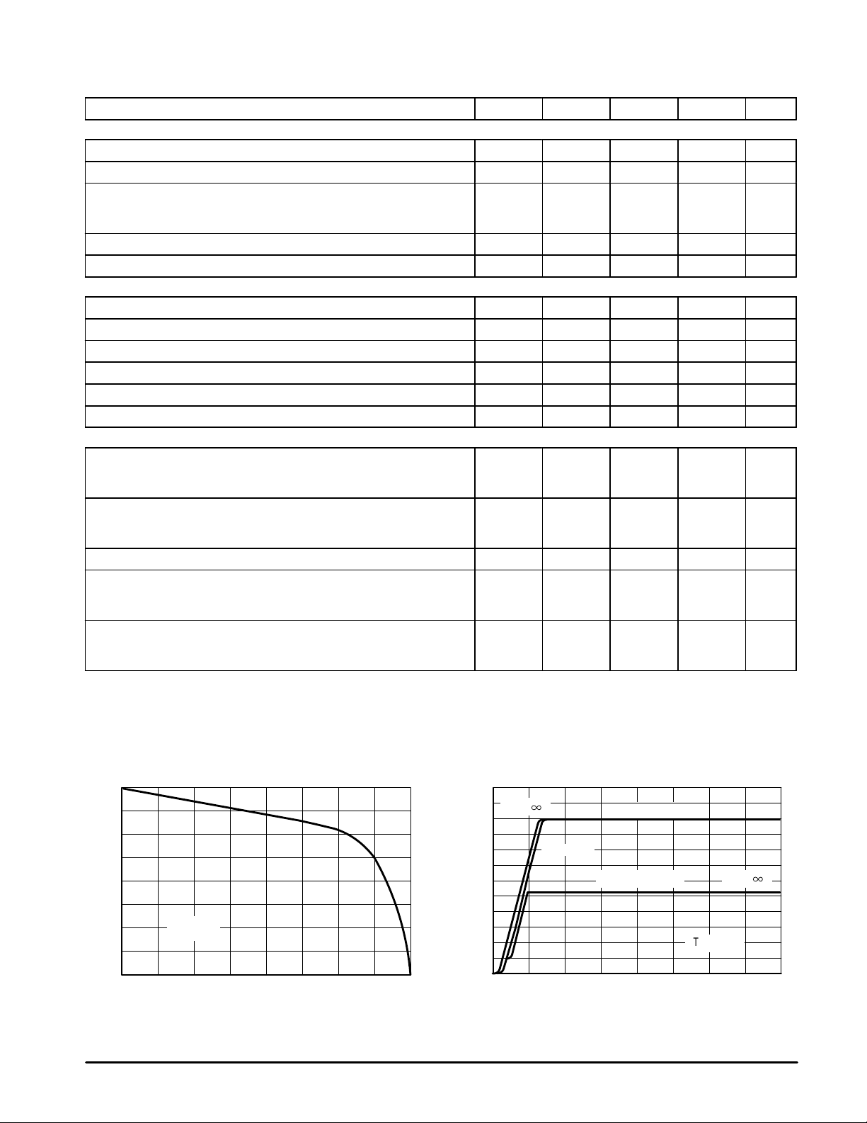
Figure 1. Regulator Output Voltage Change
versus Source Current
0
–4.0
–8.0
–12
–16
, REGULAT OR OUTPUT VOLTAGE CHANGE (mV)
O
0 40 80 120 160
V
∆
VCC = 7.5 V
°
C
TA = 25
IO, REGULAT OR OUTPUT SOURCE CURRENT (mA)
MOTOROLA ANALOG IC DEVICE DATA
Figure 2. Reference and Regulator Output
versus Supply V oltage
6.0
RL =
1
4.0
2.0
OUTPUT VOLTAGE (V)
0
0 10203040
RL = 50
Regulator Output
Ω
Reference Output RL =
TA = 25°C
VCC, SUPPLY VOLTAGE (V)
1
3
Page 4
MC34160 MC33160
Figure 3. Reference Output V oltage Change
versus Source Current
0
–8.0
–16
–24
, REFERENCE OUTPUT VOLTAGE CHANGE (mV)
–32
ref
0 2.0 4.0 6.0 8.0
V
∆
VCC = 7.5 V
°
C
TA = 25
I
, REFERENCE OUTPUT SOURCE CURRENT (mA)
ref
Figure 5. Power Warning Comparator Delay
versus T emperature
800
VCC = 30 V
Vin (Pin 9) = 2.5 V to 2.7 V
RL = 2.4 k to V
600
O
Output Rise
Figure 4. Power Warning Hysteresis Current
versus Programming Resistor
60
µ
VCC = 30 V
V
= 2.5 V
Pin 9
°
C
TA = 25
40
20
, HYSTERESIS CURRENT ( A)
H
I
0
20 40 60 80 100 120 140
RH, PROGRAMMING RESISTOR (kW)
Figure 6. Uncommitted Comparator Delay
versus T emperature
440
VCC = 30 V
V
= 2.5 V to 2.9 V
V
360
RL = 2.4 k to V
Pin 1
Pin 2
= 2.6 V
O
Output Rise
Output Fall
400
, OUTPUT DELA Y TIME (ns)
DLY
t
200
–55 –25 0 25 50 75 100 125
TA, AMBIENT TEMPERATURE (
°
C)
Figure 7. Comparator Output Saturation
versus Sink Current
0.5
VCC = 6.0 V
V
= V
Pin 1
0.4
V
V
0.3
0.2
, OUTPUT SA TURATION (V)
OL
0.1
V
0
0 2.0 4.0 6.0 8.0
ref
= 10 kΩ to Gnd
Pin 2, 9
= Pins 6, 7, 8
sat
TA = 85
TA = 25
°
C
I
, SINK CURRENT (mA)
Sink
°
C
TA = –40
280
Output Fall
, OUTPUT DELA Y TIME (ns)
200
DLY
t
120
–55 –25 0 25 50 75 100 125
TA, AMBIENT TEMPERATURE (°C)
Figure 8. P Suffix (DIP–16) Thermal Resistance and
Maximum Power DIssipation versus
P.C.B. Copper Length
°
100
Printed circuit board heatsink example
80
R
θ
60
°
C
40
20
00
, THERMAL RESISTANCE JUNCTION TO AIR ( C/W)
JA
θ
R
JA
P
for TA = 70°C
D(max)
10020304050
L, LENGTH OF COPPER (mm)
2.0 oz.
L
Copper
L
Graphs represent symmetrical layout
3.0 mm
5.0
4.0
3.0
2.0
1.0
, MAXIMUM POWER DISSIPATION (W)
D
P
4
MOTOROLA ANALOG IC DEVICE DATA
Page 5

MC34160 MC33160
Figure 9. DW Suffix (SOP–16L) Thermal Resistance and
Maximum Power Dissipation versus P.C.B. Copper Length
100
90
P
D(max)
for TA = 50°C
2.8
2.4
80
°
70
60
50
JA
JUNCTION-TO-AIR ( C/W)
θ
R , THERMAL RESISTANCE
40
30
02030504010
Graph represents symmetrical layout
2.0 oz.
L
Copper
R
θ
JA
L, LENGTH OF COPPER (mm)
3.0 mmL
2.0
1.6
1.2
0.8
0.4
0
, MAXIMUM POWER DISSIPATION (W)
D
P
PIN FUNCTION DESCRIPTION
Pin Function Description
1 Comparator Inverting Input This is the Uncommitted Comparator Inverting input. It is typically connected to a resistor
2 Comparator Noninverting Input This is the Uncommitted Comparator Noninverting input. It is typically connected to a
3 N.C. No connection. This pin is not internally connected.
4, 5, 12, 13 Gnd These pins are the control circuit grounds and are connected to the source and load
6 Comparator Output This is the Uncommitted Comparator output. It is an open collector sink–only output
7 Reset This is the Reset Comparator output. It is an open collector sink–only output requiring a
8 Power Warning This is the Power Warning Comparator output. It is an open collector sink–only output
9 Power Sense This is the Power Warning Comparator noninverting input. It is typically connected to a
10 Hysteresis Adjust The Power Warning Comparator hysteresis is programmed by a resistor connected from
11 Regulator Output This is the 5.0 V Regulator output.
14 V
15 Chip Disable This input is used to switch the IC into a standby mode turning off all outputs.
16 V
CC
ref
divider to monitor a voltage.
reference voltage.
ground returns. They are part of the IC lead frame and can be used for heatsinking.
requiring a pull–up resistor.
pull–up resistor.
requiring a pull–up resistor.
resistor divider to monitor the input power source voltage.
this pin to ground.
This pin is the positive supply input of the control IC.
This is the 2.6 V Reference output. It is intended to be used in conjunction with the Power
Warning and Uncommitted comparators.
OPERA TING DESCRIPTION
The MC34160 series is a monolithic voltage regulator and
supervisory circuit containing many of the necessary
monitoring functions required in microprocessor based
systems. It is specifically designed for appliance and
industrial applications, offering the designer a cost effective
solution with minimal external components. These devices
are specified for operation over an input voltage of 7.0 V to
40 V, and with a junction temperature of –40° to +150°C. A
typical microprocessor application is shown in Figure 10.
Regulator
The 5.0 V regulator is designed to source in excess of
100 mA output current and is short circuit protected. The
output has a guaranteed tolerance of ±5.0% over line, load,
and temperature. Internal thermal shutdown circuitry is
included to limit the maximum junction temperature to a safe
MOTOROLA ANALOG IC DEVICE DATA
level. When activated, typically at 170°C, the regulator output
turns off.
In specific situations a combination of input and output
bypass capacitors may be required for regulator stability. If
the regulator is located an appreciable distance (≥ 4″) from
the supply filter, an input bypass capacitor (Cin) of 0.33 µF or
greater is suggested. Output capacitance values of less than
5.0 nF may cause regulator instability at light load (≤ 1.0 mA)
and cold temperature. An output bypass capacitor of 0.1 µF
or greater is recommended to ensure stability under all load
conditions. The capacitors selected must provide good high
frequency characteristics.
Good construction techniques should be used to minimize
ground loops and lead resistance drops since the regulator
does not have external sense inputs.
5
Page 6

MC34160 MC33160
Reference
The 2.6 V bandgap reference is short circuit protected and
has a guaranteed output tolerance of ±5.0% over line, load,
and temperature. It is intended to be used in conjunction with
the Power Warning and Uncommitted comparator. The
reference can source in excess of 2.0 mA and sink a
maximum of 10 µA. For additional current sinking capability,
an external load resistor to ground must be used.
Reference biasing is internally derived from either VCC or
VO, allowing proper operation if either drops below nominal.
Chip Disable
This input is used to switch the IC into a standby mode.
When activated, internal biasing for the entire die is removed
causing all outputs to turn off. This reduces the power supply
current (ICC) to less than 0.3 mA.
Comparators
Three separate comparators are incorporated for voltage
monitoring. Their outputs can provide diagnostic information
to the microprocessor, preventing system malfunctions.
The Reset Comparator Inverting Input is internally
connected to the 2.6 V reference while the Noninverting Input
monitors VO. The Reset
approximately 180 mV below its regulated voltage. To
prevent erratic operation when crossing the comparator
threshold, 70 mV of hysteresis is provided.
The Power Warning Comparator is typically used to detect
an impending loss of system power. The Inverting Input is
internally connected to the reference, fixing the threshold at
2.6 V. The input power source Vin is monitored by the
Noninverting Input through the R1/R2 divider (Figure 10). This
input features an adjustable 10 µA to 50 µA current sink I
that is programmed by the value selected for resistor RH. A
default current of 6.5 µA is provided if RH is omitted. When the
comparator input falls below 2.6 V, the current sink is
activated. This produces hysteresis if Vin is monitored
through a series resistor (R1). The comparator thresholds are
defined as follows:
V
th(lower)
V
th(upper)
Output is active low when VO falls
= V
= V
ref
ref
1 +
1 +
R1
R
R1
R
2
2
+ IH R
1
1
– IIB R
Figure 10. T ypical Microprocessor Application
V
CC
14
C
in
15
9
10
R
H
2
R
1
in
AC
Line
V
in
R
1
Chip
Disable
R
2
2.6 V
+
2.6 V
Reference
The nominal hysteresis current IH equals 1.2 V/R
H
(Figure 4).
The Uncommitted Comparator can be used to
synchronize the microprocessor with the ac line signal for
timing functions, or for synchronous load switching. It can
also be connected as a line loss detector as shown in
Figure 11. The comparator contains 200 mV of hysteresis
preventing erractic output behavior when crossing the input
threshold.
The Power Warning and Uncommitted Comparators each
have a transistor base–emitter connected across their inputs.
The base input normally connects to a voltage reference
while the emitter input connects to the voltage to be
monitored. The transistor limits the negative excursion on the
emitter input to – 0.7 V below the base input by supply current
from VCC. This clamp current will prevent forward biasing the
IC substrate. Zener diodes are connected to the comparator
inputs to enhance the ICs electrostatic discharge capability.
Resistors R1 and Rin must limit the input current to a
maximum of ±2.0 mA.
Each comparator output consists of an open collector NPN
transistor capable of sinking 2.0 mA with a saturation voltage
less than 0.4 V, and standing off 40 V with minimal leakage.
Internal bias for the Reset and Power Warning Comparators
is derived from either VCC or the regulator output to ensure
functionality when either is below nominal.
Heat Tab Package
The MC34160 is contained in a 16 lead plastic
dual–in–line package in which the die is mounted on a
special Heat T ab copper alloy lead frame. This tab consists of
the four center ground pins that are specifically designed to
H
improve thermal conduction from the die to the surrounding
air. The pictorial in Figure 8 shows a simple but effective
method of utilizing the printed circuit board medium as a heat
dissipator by soldering these tabs to an adequate area of
copper foil. This permits the use of standard board layout and
mounting practices while having the ability to more than halve
the junction to air thermal resistance. The example and graph
are for a symmetrical layout on a single sided board with one
ounce per square foot copper.
V
C
O
+
–
O
MPU Reset
V
ref
Power Warning
Line Sync.
Sink Only
=
Positive True Logic
I
H
+
Thermal
Shutdown
–
+
+
IH On/Off
Uncommitted
Comparator
+
–
4, 5, 12, 13
0.913 R
.01 R
R
Power
Warning
–
+
+
–
Reset
11
7
16
8
6
6
MOTOROLA ANALOG IC DEVICE DATA
Page 7

MC34160 MC33160
Figure 11. Line Loss Detector Application
Point A
Pin 6
Pin 8
AC
Line
V
t
DLY
in
Chip
Disable
≈
R
DLY CDLY
C
2.6 V
2.6 V
R
in
A
V
CC
in
R
1
ln
V
ref
+
14
2.6 V
Reference
15
9
10
2
1
IH R
– V
DLY
+ IH R1 – VO + IH R
V
11
+
–
7
Reset
10
8
6
Sink Only
=
Positive True Logic
–
+
+
IH On/Off
Uncommitted
Comparator
+
–
4, 5, 12, 13
0.913 R
.01 R
R
Power
Warning
+
–
+
–
Thermal
Shutdown
I
H
+
O
DLY
O
C
O
MPU Reset
V
ref
Line Loss Output
R
DLY
C
DLY
Figure 12. Time Delayed Microprocessor Reset
V
V
in
R
1
Chip
Disable
R
2
CC
C
in
R
H
14
15
9
10
2
1
6.2 k
+
2.6 V
Reference
3.6 k
I
H
+
Thermal
Shutdown
–
+
+
IH On/Off
Uncommitted
+
–
4, 5, 12, 13
t
R
DLY
+
–
0.913 R
.01 R
R
Power
Warning
+
–
Comparator
DLY CDLY
Sink Only
=
Positive True Logic
+
–
Reset
V
C
DLY
C
O
R
DLY
O
V
ref
MPU Reset
11
7
16
8
6
MOTOROLA ANALOG IC DEVICE DATA
7
Page 8

–T–
SEATING
PLANE
MC34160 MC33160
OUTLINE DIMENSIONS
PLASTIC PACKAGE
–A–
916
–B–
18
NOTE 5
N
F
D
0.13 (0.005) T A
G
16 PL
E
M
S
–A–
916
–B–
P 8 PL
18
0.25 (0.010)
G 14 PL
C
–T–
SEATING
K
16 PL
D
0.25 (0.010) T A B
M
PLANE
S S
CASE 648C–03
C
K
PLASTIC PACKAGE
CASE 751G–02
M M
J
F
M
P SUFFIX
(DIP–16)
L
J
0.13 (0.005) T B
DW SUFFIX
(SOP–16L)
B
R
16 PL
X 45°
NOTES:
1. DIMENSIONING AND TOLERANCING PER ANSI
Y14.5M, 1982.
2. CONTROLLING DIMENSION: INCH.
3. DIMENSION L TO CENTER OF LEADS WHEN
FORMED PARALLEL.
4. DIMENSION B DOES NOT INCLUDE MOLD
FLASH.
5. INTERNAL LEAD CONNECTION, BETWEEN 4
AND 5, 12 AND 13.
INCHES
MIN MINMAX MAX
DIM
0.740
A
0.240
B
0.145
C
0.015
D
E
M
M
S
NOTES:
1. DIMENSIONING AND TOLERANCING PER ANSI
Y14.5M, 1982.
2. CONTROLLING DIMENSION: MILLIMETER.
3. DIMENSIONS A AND B DO NOT INCLUDE MOLD
PROTRUSION.
4. MAXIMUM MOLD PROTRUSION 0.15 (0.006) PER
SIDE.
5. DIMENSION D DOES NOT INCLUDE DAMBAR
PROTRUSION. ALLOWABLE DAMBAR
PROTRUSION SHALL BE 0.13 (0.005) TOTAL IN
EXCESS OF D DIMENSION AT MAXIMUM
MATERIAL CONDITION.
DIM
A
B
C
D
F
G
J
K
M
P
R
0.050 BSC
0.040
F
0.100 BSC
G
J
0.008
K
0.115
0.300 BSC
L
M
0
°
N
0.015
MILLIMETERS INCHES
MIN MINMAX MAX
10.45
10.15
7.60
7.40
2.65
2.35
0.49
0.35
0.90
0.50
1.27 BSC 0.050 BSC
0.32
0.25
0.25
0.10
7
0
°
°
10.05
10.55
0.25
0.75
0.840
0.260
0.185
0.021
0.070
0.015
0.135
10
0.040
0.400
0.292
0.093
0.014
0.020
0.010
0.004
0
0.395
0.010
°
°
MILLIMETERS
18.80
21.34
6.10
6.60
3.69
4.69
0.38
0.53
1.27 BSC
1.02
1.78
2.54 BSC
0.20
0.38
2.92
3.43
7.62 BSC
0
10
°
0.39
1.01
0.411
0.299
0.104
0.019
0.035
0.012
0.009
7
°
0.415
0.029
°
Motorola reserves the right to make changes without further notice to any products herein. Motorola makes no warranty , representation or guarantee regarding
the suitability of its products for any particular purpose, nor does Motorola assume any liability arising out of the application or use of any product or circuit, and
specifically disclaims any and all liability, including without limitation consequential or incidental damages. “T ypical” parameters which may be provided in Motorola
data sheets and/or specifications can and do vary in different applications and actual performance may vary over time. All operating parameters, including “Typicals”
must be validated for each customer application by customer’s technical experts. Motorola does not convey any license under its patent rights nor the rights of
others. Motorola products are not designed, intended, or authorized for use as components in systems intended for surgical implant into the body, or other
applications intended to support or sustain life, or for any other application in which the failure of the Motorola product could create a situation where personal injury
or death may occur. Should Buyer purchase or use Motorola products for any such unintended or unauthorized application, Buyer shall indemnify and hold Motorola
and its officers, employees, subsidiaries, affiliates, and distributors harmless against all claims, costs, damages, and expenses, and reasonable attorney fees
arising out of, directly or indirectly, any claim of personal injury or death associated with such unintended or unauthorized use, even if such claim alleges that Motorola
was negligent regarding the design or manufacture of the part. Motorola and are registered trademarks of Motorola, Inc. Motorola, Inc. is an Equal
Opportunity/Affirmative Action Employer.
How to reach us:
USA/EUROPE/Locations Not Listed: Motorola Literature Distribution; JAPAN: Nippon Motorola Ltd.; Tatsumi–SPD–JLDC, 6F Seibu–Butsuryu–Center,
P.O. Box 20912; Phoenix, Arizona 85036. 1–800–441–2447 or 602–303–5454 3–14–2 Tatsumi Koto–Ku, Tokyo 135, Japan. 03–81–3521–8315
MFAX: RMF AX0@email.sps.mot.com – TOUCHT ONE 602–244–6609 ASIA/PACIFIC: Motorola Semiconductors H.K. Ltd.; 8B Tai Ping Industrial Park,
INTERNET: http://Design–NET.com 51 Ting Kok Road, T a i Po, N.T., Hong Kong. 852–26629298
8
◊
MOTOROLA ANALOG IC DEVICE DATA
MC34160/D
*MC34160/D*
 Loading...