

Page 1
MC33157
Half Bridge Controller and
Driver for Industrial
Linear Tubes
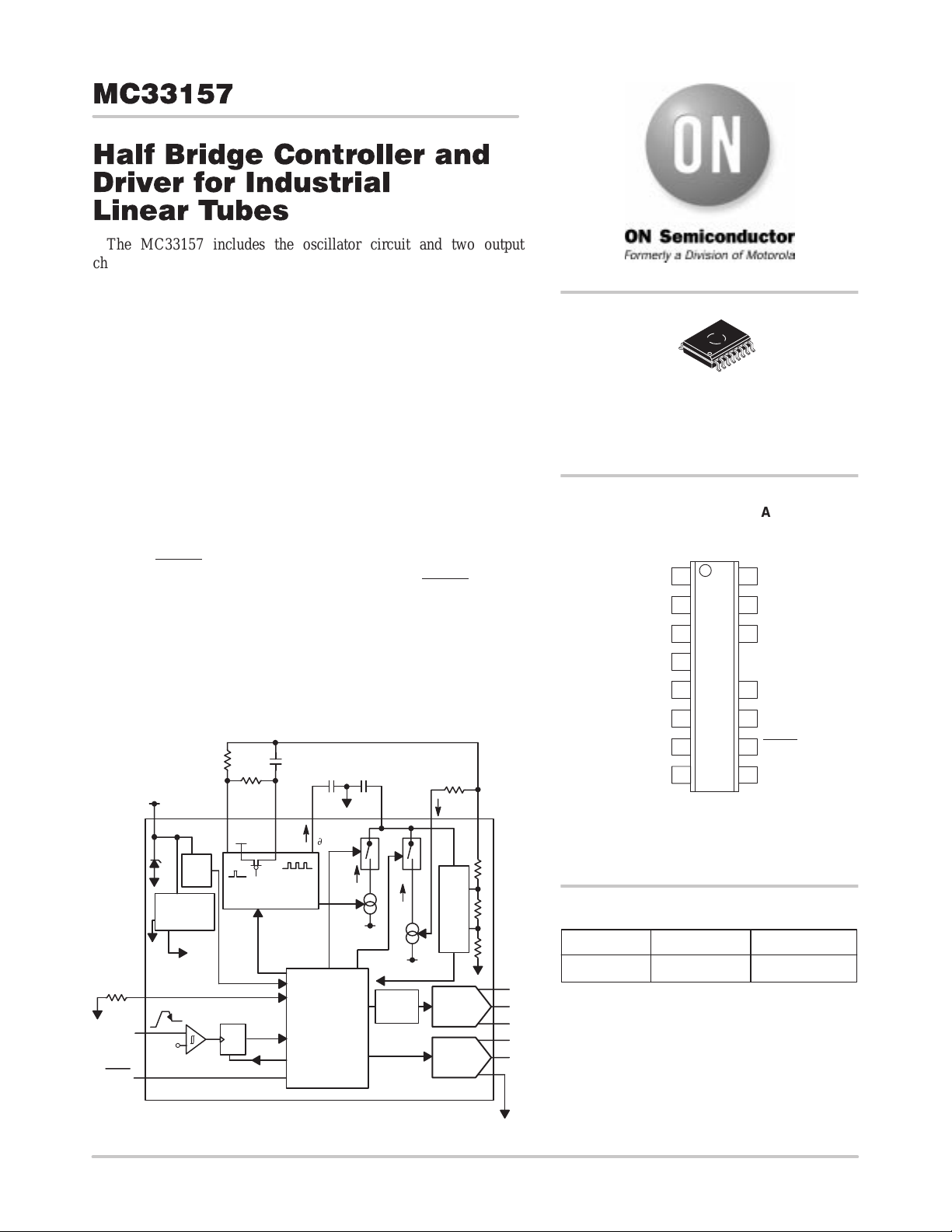
The MC33157 includes the oscillator circuit and two output
channels to control a half–bridge power stage.
One of the channels is ground–referenced. The second one is
floating to provide a bootstrap operation for the high side switch.
Dedicated Driver for Industrial Linear T ubes
• Main oscillator is current controlled, making it easy to set up by a
single external resistor . On top of that, such a feature is useful to
implement a dimming function by frequency shift.
• Filament pre–heating time control built–in.
• The strike sequence is controllable by external passive components,
the resonnant frequency being independently adjustable. This
frequency can be made different from the pre–heating and the steady
state values. A frequency sweep between two defined values makes
this IC suitable for any series resonnant topologies.
• Dedicated internal comparator provides an easy lamp strike detection
implementation.
• Digital RESET pin provides a fast reset of the system (less than 10µs).
Both output MOSFET are set to “OFF” state when RESET is zero.
• Adjustable dead time makes the product suitable for any snubber
capacitor and size of MOSFET used as power switches.
• Designed to be used with standard setting capacitors ≤ 470nF.
• A voltage reference, derived from the internal bandgap, is provided
for external usage. This voltage is 100% trimmed at probe level
yielding a 2% tolerance over the temperature range.
C
PH
SWEEP
C
PH
Iph
ē
Iph
Ifstrike
ENABLE
Dead Time
CONTROL LOGIC
Strike Detection
Clear
INHIBIT
+Vref
C
OP
SHIFTER
Iop
LEVEL
+Vref
R
OP
ICO
COMPARATOR
HIGH SIDE
BUFFER
LOW SIDE
BUFFER
+Vref
2
R
R
R
16
VHS
15
VHO
14
VOUT
13
NC
12
VLO
11
GND
DT adjust
Strike
Detection
RESET
R
ENDSWP
U
VLO
+Vref
(+7 V)
R
+Vref
PREHEAT
& STRIKE CONTROL
Latch
Q
C
V
DD
145367
15 V
BAND GAP
REFERENCE
8
9
Vth
10
http://onsemi.com
16
1
SO–16L
DW SUFFIX
CASE 751G
PIN CONNECTIONS AND
MARKING DIAGRAM
116
V
DD
2
+V
ref
C
3
PH
R
4
PH
C
SWEEP
512
MC33157DW
6
C
OP
ICO
7
DTA SD
AWL = Manufacturing Code
YYWW = Date Code
(Top View)
15
14
AWLYYWW
11
10
98
V
HS
V
HO
V
OUT
V
LO
GND
RESET
ORDERING INFORMATION
Device Package Shipping
MC33157DW Plastic SO–16L 47 Units / Rail
Semiconductor Components Industries, LLC, 1999
November, 1999 – Rev. 1
1 Publication Order Number:
MC33157/D
Page 2
MC33157
Á
Á
Á
Á
Á
Á
Á
Á
Á
Á
Á
Á
Á
Á
Á
Á
Á
Á
Á
Á
Á
Á
Á
Á
Á
Á
Á
Á
Á
Á
Á
Á
MAXIMUM RATINGS
Rating Symbol Value Unit
High Side Max Voltage
Differential Max Voltage VHS – V
High Side Output Voltage Range
Low Side Output Voltage Range
Max VHS Allowable Slew Rate
Max VHO/VLO Allowable Slew Rate
Supply Voltage
Maximum Power Dissipation @ TA = 50°C
ББББББББББББББББ
Thermal Resistance Junction–to–Air
Operating Junction Temperature
ББББББББББББББББ
(Note 1)
Storage Temperature Range
Electrostatic Discharge [HBMI]
OUT
V
HS
D
V
HS
V
HO
V
LO
dVHS/dt
dVHO/dt, dVLO/dt
V
DD
P
БББББ
БББББ
D
R
θJA
T
J
T
stg
ESD
600
16
V
–0.3 to VHS+0.3
OUT
–0.3 to +16
±10
±10
16
ББББББ
ББББББ
600
140
–40 to +150
–65 to +150
2.0
V/ns
V/ns
mW
Á
°C/W
Á
V
V
V
V
V
°C
°C
kV
ELECTRICAL CHARACTERISTICS (V
= 14V . All parameters are specified for –20 °C to 85°C ambient temperature
DD
unless otherwise noted.)
Characteristic
SUPPLY VOLTAGE
Input Threshold Voltage
Turn–On
ББББББББББББББББ
Turn–Off
Clamp Voltage @ I
Supply Current
(Note 2)
Standby Current at No Load @ VDD < UV
Quiescent Current at No Load @ VDD > UV
CLAMP
= 10 mA
OFF
ON
OUTPUT DRIVERS (VLO, VHO)
High Side VDSON @ Source current = 250 mA
Low Side VDSON @ Sink current = 300 mA
High Side / Low Side rise time @ C
High Side / Low Side fall time @ C
OUT
OUT
= 2 nF
= 2 nF
OSCILLATOR
Output Max Frequency
Internal Master Clock Duty Cycle
System operation programming recommended values
ББББББББББББББББ
ББББББББББББББББ
ББББББББББББББББ
V
High threshold
COP
V
Low threshold
COP
I
discharging current
COP
I
COP
over I
current ratio
ROP
Symbol Min Typ Max Unit
UV
ON
ÁÁÁ
UV
OFF
V
CLAMP
I
S
I
STDBY
I
Q
VDS(P)
VDS(N)
t
r
t
f
f
OSC
DC
R
OP
ÁÁÁ
R
PH
R
ENDSWEEP
ÁÁÁ
R
DTA
ÁÁÁ
C
OP
11
ÁÁ
8.0
15
–
–
–
68
ÁÁ
68
68
ÁÁ
10
ÁÁ
100
–
–
–
–
12
ÁÁ
8.5
16
12
1.5
2.5
880
880
40
35
50
ÁÁ
ÁÁ
ÁÁ
4.2
2.8
400
2.0
12.8
ÁÁ
9.0
16.5
1500
1500
250
–
560
ÁÁ
560
2200
ÁÁ
250
ÁÁ
560
–
–
–
–
Á
mA
mA
mA
mV
mV
ns
ns
kHz
%
k
Á
k
k
Á
k
Á
pF
µA
V
V
V
W
W
W
W
V
V
http://onsemi.com
2
Page 3
MC33157
ELECTRICAL CHARACTERISTICS (continued) (V
unless otherwise noted.)
Characteristic UnitMaxTypMinSymbol
TIMING
Preheat timing capacitor pulsed charging current
(Duty Cycle=1/16)
Filament preheat time with CPH = 0.47 µF
Strike sequence recycling time with CPH = 0.47 µF
CPH charging current ratio
Strike sequence restart blanking time with CPH = 470nF
Dead time: externally adjustable by Rdt
Dead time adjust resistance (Recommended range)
Dead time tolerance
VOLTAGE REFERENCE
Voltage reference @ I
Line regulation @ I
Load regulation @ I
Maximum load current
Total V
REF
INPUT
Strike detect high voltage threshold
Strike detect low voltage threshold
Maximum current on strike detect input @ Regulation level ISDHI – – 10 nA
Maximum voltage on strike detect @ Regulation level VSDHI – – 7.0 V
Maximum current on strike detect input @ Low level ISDLO – – 10 nA
Maximum strike detect voltage negative input VSDNEG – – –0.3 V
Strike detect minimum pulse width
RESET high voltage
RESET low voltage
RESET input current @ high voltage
RESET input current @ low voltage
RESET maximum voltage
RESET maximum negative voltage
NOTES:
(1) Since this device has a built–in zener, one cannot use a low impedance supply to drive this pin. Having a current limit mode by external
means is mandatory.
(2) Test Conditions: C
LOAD
variation over Line, Temperature, Load
OUT
= 500 µA, TJ = 25°C
LOAD
= 500 µA, TJ = 25°C
= 500 µA to 5 mA
LOAD
= 2.2 nF, f = 100 kHz, VDD = 15V.
= 14V . All parameters are specified for –20 °C to 85°C ambient temperature
DD
It
PH
t
PH
t
SK
∂
t
bk
dt
Rdt
dt
Tol
V
REF
D
V
REF
D
V
REF
I
REFMAX
V
REF
VTHSDHI
VTHSDLO
SDPW
RSTHI
RSTLO
14
–
–
–
–
0.3
10
–
–
–
–
6.85
–
–
50
–
1.6
–
–
–
–
16
2.0
125
1/16
10
–
–
±10
7.0
10
10
–
7.0
4.0
3.75
100
1.8
1.8
–20
–20
–
–
17
–
–
–
–
2.5
220
–
–
–
25
7.15
–
–
–
2.2
–
–
–
7.0
–0.3
µA
s
ms
ms
µs
k
%
V
mV
mV
mA
V
V
V
ns
V
V
µA
µA
V
V
W
http://onsemi.com
3
Page 4
Á
Á
Á
Á
Á
Á
Á
Á
Á
Á
Á
Á
Á
Á
Á
Á
Á
Á
Á
Á
Á
Á
Á
Á
Á
Á
Á
Á
Á
Á
Á
Á
Á
Á
Á
Á
Á
Á
Á
Á
Á
Á
Á
Á
Á
Á
Á
Á
Á
Á
Á
Á
Á
Á
Á
Á
Á
Á
Á
Á
Á
Á
Á
Á
Á
Á
Á
Á
Á
Á
Á
Á
Á
Á
Á
Á
Á
Á
Á
Á
Á
Á
Á
Á
Á
Á
Á
Á
Á
Á
Á
Á
Á
Á
Á
Á
Á
Á
Á
Á
Á
Á
Á
Á
Á
Á
Á
Á
Á
Á
Á
Á
Á
Á
Á
Á
MC33157
PIN FUNCTION DESCRIPTION
Pin Symbol Function Description
1
Á
Á
Á
Á
Á
Á
Á
Á
Á
Á
Á
Á
Á
Á
Á
Á
Á
Á
Á
Á
Á
10
Á
Á
Á
Á
Á
Á
Á
Á
V
DD
ÁÁ
ÁÁ
2
+V
ÁÁ
3
C
PH
ÁÁ
ÁÁ
4
R
PH
ÁÁ
ÁÁ
ÁÁ
5
C
SWEEP
ÁÁ
ÁÁ
6
C
OP
ÁÁ
ÁÁ
7
ICO
ÁÁ
ÁÁ
8
DTA
ÁÁ
9
SD
ÁÁ
ÁÁ
ÁÁ
ÁÁ
ÁÁ
ÁÁ
RESET
ÁÁ
ÁÁ
ÁÁ
ÁÁ
ÁÁ
ÁÁ
ÁÁ
ÁÁ
ref
Supply voltage
input
ÁÁÁ
ÁÁÁ
Voltage
reference
ÁÁÁ
output
Preheat timing
ÁÁÁ
capacitor
ÁÁÁ
Preheat and
ÁÁÁ
Strike
frequencies
ÁÁÁ
adjustment
resistors
ÁÁÁ
Frequency
sweep timing
ÁÁÁ
capacitor
ÁÁÁ
Oscillator
capacitor
ÁÁÁ
ÁÁÁ
Steady state
operating
ÁÁÁ
frequency
adjustment
ÁÁÁ
current input
Dead Time
ÁÁÁ
Adjust
Strike detection
input
ÁÁÁ
ÁÁÁ
ÁÁÁ
ÁÁÁ
ÁÁÁ
ÁÁÁ
Master reset
input
ÁÁÁ
ÁÁÁ
ÁÁÁ
ÁÁÁ
ÁÁÁ
ÁÁÁ
ÁÁÁ
ÁÁÁ
This pin provides the DC supply to the circuit. The voltage is internally clamped by a zener
connected to the ground. It is NOT allowed to use a DC low impedance power supply to feed this
ББББББББББББББББББББББ
pin, but limiting the current by an external resistor is mandatory. It is recommended to damp this pin
ББББББББББББББББББББББ
to ground by an electrolytic capacitor connected close to pin 1.
This pin provides a +7V voltage reference derived from the internal bandgap. The +Vref can supply
up to 25 mA and shall be decoupled to ground by a 220nF ceramic capacitor
ББББББББББББББББББББББ
This capacitor sets two timings: filaments preheat time (tPH) and strike sequence recycle time (tSK).
ББББББББББББББББББББББ
It is charged with a constant current and cares must be observed to minimize the leakage current
at this pin to get the expected timing. Typically, a 0.47 µF capacitor will give a 2 seconds
ББББББББББББББББББББББ
pre–heating time and a 125 ms strike sequence recycle time. (See details given by figure 9)
The RPH resistor together with R
ББББББББББББББББББББББ
filaments (fPH = f1). R
timing, the frequency will sweep from the high pre–heating f1 to the low strike f2 values. Normally,
ББББББББББББББББББББББ
f1 is far from the LC resonance but f2 is close enough to generate the high voltage across the
fluorescent tube. (See details given by figure 9)
ББББББББББББББББББББББ
ENDSWEEP
ENDSWEEP
defines the strike frequency (f
This timing define the sweep time from f1 to f2. Since the timing capacitor is charged with a low
constant current, cares must be observed to minimize the leakage current at this pin to get the
ББББББББББББББББББББББ
expected timing. Since this capacitor is charged through resistor RPH, the voltage rises according
to an exponential and the frequency shifts with the same law.
ББББББББББББББББББББББ
This pin defines the steady state operation frequency (f3 = fOP) of the controller. Since this timing
capacitor is charged with a low constant current, cares must be observed to minimize the leakage
ББББББББББББББББББББББ
current at this pin to get the expected frequency. Film type capacitor are recommended
(polycarbonate).
ББББББББББББББББББББББ
Since the circuit uses a Current Controlled Oscillator (ICO), the current forced into this pin will
control the operating frequency. The allowable current range is from 1 µA to 500 µA. The +Vref
ББББББББББББББББББББББ
output can be used to provide the voltage across ROP. An auxiliary voltage source can be used to
implement a dimming function.
ББББББББББББББББББББББ
This pin provides an access to the internal timing system to adjust the dead time between the gate
ББББББББББББББББББББББ
drive of the High and Low power switches connected, respectively, to pin VHO and VLO.
This pin drives a comparator, with an internal fixed reference, and acknowledges the tube strike.
When a negative going slope (across the internal reference) is detected, the system considers the
ББББББББББББББББББББББ
lamp has struck and the oscillator jumps from the present frequency value, which is within the
ББББББББББББББББББББББ
window defined by RPH and R
going slope is detected on this pin, the system will repeat the sweep and strike sequence four
ББББББББББББББББББББББ
times, then stops. The circuit will re–start from either a RESET, or by pulling +VDD to ground. The
ББББББББББББББББББББББ
input signal can be either a logic level or an analog voltage ramping up from zero to +Vref followed
by a negative going slope to zero. In any case, the positive pulse width must be 1 µs minimum. The
ББББББББББББББББББББББ
pcb layout must be designed to minimize the noise at this pin. (See details given by figures 8, 9, &
ББББББББББББББББББББББ
10)
ENDSWEEP
Forcing a logic zero to this pin (HCMOS low level) will reset the circuit, initializing a frequency sweep
and lamp strike sequence. The master reset does not include the pre–heating timing. The minimum
ББББББББББББББББББББББ
pulse width requested is 10µs to guarantee a reset state. However, this pin has no built in filtering
ББББББББББББББББББББББ
and a shorter pulse may initialize a reset sequence: it is the responsibility of the designer to make
sure that no noise or parasitic pulse are developed at the RESET input. A full re–start of the
ББББББББББББББББББББББ
sequence, including the pre–heating time, can be initialized by pulling the +VDD pin to ground. In this
case, +VDD and RESET
ББББББББББББББББББББББ
low (active) both outputs MOS are biased in the off condition. An internal 20µA pull up current forces
ББББББББББББББББББББББ
the pin to logic one, allowing the designer to left this pin open if the RESET function is not used. In
order to avoid any uncontrolled state of the output drivers, it is recommended to set up a 10ms low
ББББББББББББББББББББББ
level at pin 10. The reset is activated in less than 10 microsecond, but releasing this pin while the Vcc
ББББББББББББББББББББББ
supply is high (above 300V) can generate a random operation, depending upon the dv/dt coming
from the power supply.
ББББББББББББББББББББББ
must be simultaneously released to a high state. When RESET is asserted
http://onsemi.com
4
and COP defines the frequency used to preheat the
ENDSWEEP
= f2). During the sweep
to the steady state value defined by ROP. If no negative
Page 5

Pin DescriptionFunctionSymbol
Á
Á
Á
Á
Á
Á
Á
Á
Á
Á
Á
Á
Á
Á
Á
Á
Á
Á
Á
Á
11
GND
Á
Á
Á
Á
Á
12
13
14
15
16
ÁÁ
V
LO
ÁÁ
NC
V
OUT
ÁÁ
ÁÁ
V
HO
ÁÁ
V
HS
Ground
(zero voltage
ÁÁÁ
reference)
Low side driver
ÁÁÁ
output
Not Connected
High side
common point /
ÁÁÁ
Half bridge
ÁÁÁ
output
High side driver
output
ÁÁÁ
High voltage
boost supply
MC33157
PIN FUNCTION DESCRIPTION (continued)
Since high and fast currents circulate in the circuit, it is mandatory to build a single ground point in
the system.
ББББББББББББББББББББББ
This pin provides the VGS to drive the Low side power MOSFET.
ББББББББББББББББББББББ
This pin is connected to the output of the half bridge and is referenced for the High side switch.
ББББББББББББББББББББББ
ББББББББББББББББББББББ
This pin provides the VGS to drive the High side power MOSFET.
ББББББББББББББББББББББ
The gate drive of the High side switch is derived from this voltage.
http://onsemi.com
5
Page 6

+Vref
C
OP
External
MC33157
Internal
6
10 V
ESD
2K
10 V
ESD
Figure 1. PIN 6 COP INPUT
+Vref
I
I
PH
SWP
(8 UA)
Circuits
CAN’T READ
0V
ph/swp Switch
I
blanking
(200 uA)
10 V
ESD
2K
10 V
ESD
3
C
PH
(external)
Figure 2. PIN 3 CPH INPUT
+Vref
Internal
Circuits
5V
10
10 V
ESD
2K
10 V
ESD
Figure 3. PIN 10 RESET
4 V
+Vref
0.0 V
10 V
ESD
2K
10 V
ESD
9
Internal
Circuits
Hysteresis Switch
Figure 4. PIN 9 SD
http://onsemi.com
6
Page 7

MC33157
+Vref
81
2
R
OP
(external)
7
ph/swp switch
2K
10 V
ESD
R
DTA
(external)
I
8
10 V
ESD
10 V
ESD
(external)
(external)
I I/8
10 V
ESD
Internal
Circuits
10 V
ESD
2K
Figure 5. PIN 8 DTA
+Vref
10 V
ESD
2K
10 V
ESD
1 k
W
(internal)
1 k
W
(internal)
6
2I
C
OP
(external)
Figure 6. PIN ICO
+Vref
10 V
ESD
10 V
ESD
I
2K
10 V
ESD
6
2I
C
SWP
5
R
PH
2
R
4
ENDSWEEP
(external)
SD max
1 k
W
(internal)
Figure 7. PIN 2, 4 & 5 V
V
T 1 stw
ref
m
SDHIVth
4 V typ
Internal Hysterisis
The Strike Detect is acknowledged as soon as the input
voltage drops below SDLOVth. It is not necessary to pull
the input voltage to zero volt or to a negative bias
Figure 8. STRIKE DETECTION
http://onsemi.com
7
, RPH & C
SDNEG max
1 k
(internal)
SWP
W
SDLOVth
3.75 V typ
C
OP
(external)
Page 8

MC33157
Rise time
V
DD
U
VON
9.2 V typ
U
VLO
3.8 V typ
V
V
CPH
(PREHEAT)
Frequency
SWEEP
STRIKE
DETECTION
RESET
Output
Frequency
status
w
lms
ref
1
0
OFF STATE
f1 = fPH, preheating frequency adjusted by RPH and R
f2 = f
ENDSWEEP
f3 = fOP, operating frequency controlled by the ICO current (pin 7) and capacitor C
tPH = (CPH * 2/3 * Vref) / (ē * I
“OFF” state: High side switch OFF, Low side switch ON
tph
t 1 swm
STRIKE
F1 F2 F3 F1 F2 F3
, end of sweep frequency, adjusted by R
tPH
FSwp
ENDSWEEP
ENDSWEEP (
)
U RESET
VLO
7.0 V typ
OFF STATE
pin 2). In any case f1 w f
OP
FSwp
time
2
RESET
+V
ref
V
CSWP
STRIKE
DETECTION
Output Frequency
status
Figure 9. TIMING DIAGRAM (Normal startup sequence and U
10 swm
1
0
SD
HIGH
F3
Previous On state
When RESET
then executes a frequency sweep down to f
detection signal is applied to pin 9. There is no preheating timing performed after a reset coming from pin 10.
RESET
Note: Strike detection lever can be either digital – CMOS or analog as depicted here above, as long as the
signal fulfills the SD
OFF STATE: both output MOSFET are biased in the off condition.
pin is released to a logic one, the system jumps to the preheat frequency as defined by RPH,
logic level is CMOS compatible.
HIGH
OFF STATE
and SD
ENDSWEEP
values and timing.
LOW
FSweep
, as defined by R
SD
ENDSWEEP
LOW
, and waits until a strike
VLO
F3
reset)
V repeats indefinitely
CSWP
No further logic action activated
time
Figure 10. TIMING DIAGRAM (External reset)
http://onsemi.com
8
Page 9

RESET
+V
ref
V
CSWP
+VV
w
ref
STRIKE
DETECTION
MC33157
1
0
End of preheating sequence
Blanking 10 ms typ
@ C = 470 nF
PH
t
F
t
FEND
t
SK
SD
Blanking
HIGH
SD
Last restrike valid cycle
LOW
Frequency status
The controller repeats the f
Following a non strike situation, the controller goes in a full STOP and can be reinitialized by either pulling the VDD pin 1 to ground or by forcing a low to the RESET
pin 9. The controller assumes the lamp has struck when a negative going transient is applied on the STRIKE detection pin 10. On the other hand, in order to avoid false
strike information, the controller force a blank time between the end of t
Output
FSweep FSweep FSweep
tSF: Sweep Frequency time. This time is given by the RC network built with C
tSK: Sweep sequence recycle time. This time is derived by integrating a constant DC current in capacitor
C
There is a fixed ratio (ē ) between the preheating time tPH and strike sequence recycle time tSK.
PH.
t
fEND
and the strike sequence until there is a STRIKE signal coming from the external circuit, or until FOUR sequences have been counted.
SWEEP
FSweep
F2
F1
: Time during which f = (f
F2 F1 F2 F1 F2 F3
). This time is equal to tSK – tSF.
ENDSWP
and the start of the next sequence.
SWEEP
SWEEP
time
and RPH.
Figure 11. TIMING DIAGRAM (no strike conditions)
5
4.5
I = V/√ [(R2 + (Lw – 1/Cw)2]
4
3.5
I = V/√ [(R2 + (Lw)2]
Z @ RLCF
Z = Lw
3
2.5
2
Current (A)
1.5
1
0.5
0
5000
9000
13000
17000
21000
25000
29000
33000
37000
41000
45000
49000
53000
57000
61000
Frequency (F)
Figure 12. OUTPUT = f (freq) @ Lc = 1.5 mH, Cs = 6.8 nF
http://onsemi.com
9
65000
69000
73000
77000
93000
81000
85000
89000
97000
Page 10

C3
10 F/25 V
m
MC33157
+400 V
R3
C4
R4
72116
I
C2
C1
R2
R1
C6
R5
Typical Values for FPH = 70 kHz, FOP = 45 kHz, tPH = 2 s, t
T1 Np = R1 390 k
Ns = R2 62 k
Lp = 150 mH R3 100 kW – 0.5 W C3 10 mF/25 V/Electrolytic
Q1 MTP6N60E R4 100 k
Q2 MTP6N60E R5 82 K
D1 MUR160RL R6 1 M
D2 MUR120RL R7 68 K
D3 1N4148 R8 68 k
U1 MC33157 R9 22
C
6
0
C
OP
3
C
PH
4
R
PH
5
C
SWP
8
D
TA
RESET GND SD
W
W
W
W
W
W
W
W
+V
REF
MC33157
10 11 9
D1 MUR160
V
DD
U1
= 125 ms
SWEEP
C1 470 nF/25 V/Polyester
C2 470 pF/2%/50 ppm
C4 220 nF/Polyester
C5 100 nF/63 V/Polyester
C6 220 nF/25 V/Polyester
C7 6.8 nF/5%/1000 V
C8 100 nF/400 V/Polyester
C9 100 nF/400 V/Polyester
C10 22 mF/450 V/Electrolytic
C11 100 nF/25 V/Polyester
C12 330 pF/500 V/Polyester
R9
100 nF/400 V
C9
V
HS
V
HO
V
OUT
V
LO
MTP6N60E
15
14
MTP6N60E
12
Q1
Q2
C5 100 nF
330 pF
C12
Ns
Np
C11
C7
T1
D3 1N4148
R8
100 nF
100 nF/400 V
C8
R6
R7
m
22 F/450 V
C10
TO SEE: AN1682 (Using the MC33157 Electronic Ballast Controller)
Figure 13. T ypical Application Schematic Diagram
http://onsemi.com
10
Page 11

MC33157
P ACKAGE DIMENSIONS
SO–16L
DW SUFFIX
PLASTIC P ACKAGE
CASE 751G–03
ISSUE B
16 9
M
B
H8X
M
0.25
0.25 B
14X
D
B16X
M
S
A
T
e
A
q
NOTES:
1. DIMENSIONS ARE IN MILLIMETERS.
2. INTERPRET DIMENSIONS AND TOLERANCES
PER ASME Y14.5M, 1994.
E
_
h X 45
81
B
S
A
L
A1
T
SEATING
PLANE
C
3. DIMENSIONS D AND E DO NOT INLCUDE MOLD
PROTRUSION.
4. MAXIMUM MOLD PROTRUSION 0.15 PER SIDE.
5. DIMENSION B DOES NOT INCLUDE DAMBAR
PROTRUSION. ALLOWABLE DAMBAR
PROTRUSION SHALL BE 0.13 TOTAL IN EXCESS
OF THE B DIMENSION AT MAXIMUM MATERIAL
CONDITION.
MILLIMETERS
DIM MIN MAX
A 2.35 2.65
A1 0.10 0.25
B 0.35 0.49
C 0.23 0.32
D 10.15 10.45
E 7.40 7.60
e 1.27 BSC
H 10.05 10.55
h 0.25 0.75
L 0.50 0.90
q
0 7
__
http://onsemi.com
11
Page 12

MC33157
ON Semiconductor and are trademarks of Semiconductor Components Industries, LLC (SCILLC). SCILLC reserves the right to make changes
without further notice to any products herein. SCILLC makes no warranty , representation or guarantee regarding the suitability of its products for any particular
purpose, nor does SCILLC assume any liability arising out of the application or use of any product or circuit, and specifically disclaims any and all liability ,
including without limitation special, consequential or incidental damages. “Typical” parameters which may be provided in SCILLC data sheets and/or
specifications can and do vary in different applications and actual performance may vary over time. All operating parameters, including “Typicals” must be
validated for each customer application by customer’s technical experts. SCILLC does not convey any license under its patent rights nor the rights of others.
SCILLC products are not designed, intended, or authorized for use as components in systems intended for surgical implant into the body, or other applications
intended to support or sustain life, or for any other application in which the failure of the SCILLC product could create a situation where personal injury or
death may occur. Should Buyer purchase or use SCILLC products for any such unintended or unauthorized application, Buyer shall indemnify and hold
SCILLC and its officers, employees, subsidiaries, affiliates, and distributors harmless against all claims, costs, damages, and expenses, and reasonable
attorney fees arising out of, directly or indirectly , any claim of personal injury or death associated with such unintended or unauthorized use, even if such claim
alleges that SCILLC was negligent regarding the design or manufacture of the part. SCILLC is an Equal Opportunity/Affirmative Action Employer .
PUBLICATION ORDERING INFORMATION
USA/EUROPE Literature Fulfillment:
Literature Distribution Center for ON Semiconductor
P.O. Box 5163, Denver, Colorado 80217 USA
Phone: 303–675–2175 or 800–344–3860 Toll Free USA/Canada
Fax: 303–675–2176 or 800–344–3867 Toll Free USA/Canada
Email: ONlit@hibbertco.com
Fax Response Line*: 303–675–2167
800–344–3810 Toll Free USA/Canada
*To receive a Fax of our publications
N. America Technical Support: 800–282–9855 Toll Free USA/Canada
http://onsemi.com
ASIA/PACIFIC: LDC for ON Semiconductor – Asia Support
Phone: 303–675–2121 (Tue–Fri 9:00am to 1:00pm, Hong Kong Time)
Email: ONlit–asia@hibbertco.com
JAPAN: ON Semiconductor, Japan Customer Focus Center
4–32–1 Nishi–Gotanda, Shinagawa–ku, T okyo, Japan 141–8549
Phone: 81–3–5487–8345
Email: r14153@onsemi.com
ON Semiconductor Website: http://onsemi.com
For additional information, please contact your local Sales Representative.
MC33157/D
12
 Loading...