

Page 1
The MC33153 is specifically designed as an IGBT driver for high power
applications that include ac induction motor control, brushless dc motor
control and uninterruptable power supplies. Although designed for driving
discrete and module IGBTs, this device offers a cost effective solution for
driving power MOSFETs and Bipolar Transistors. Device protection features
include the choice of desaturation or overcurrent sensing and undervoltage
detection. These devices are available in dual–in–line and surface mount
packages and include the following features:
• High Current Output Stage: 1.0 A Source/2.0 A Sink
• Protection Circuits for Both Conventional and Sense IGBTs
• Programmable Fault Blanking Time
• Protection against Overcurrent and Short Circuit
• Undervoltage Lockout Optimized for IGBT’s
• Negative Gate Drive Capability
• Cost Effectively Drives Power MOSFETs and Bipolar Transistors
Order this document by MC33153/D
SINGLE IGBT
GATE DRIVER
SEMICONDUCTOR
TECHNICAL DATA
8
1
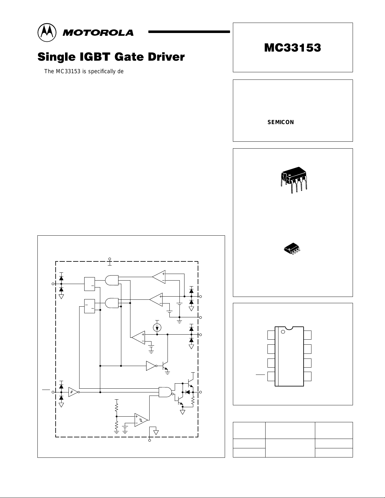
Representative Block Diagram
V
CC
6
V
CC
Short Circuit
V
V
V
EE
CC
EE
Latch
Q
Overcurrent
Latch
Q
Fault
Output
7
Input
4 5
V
CC
S
R
S
R
V
CC
This device contains 133 active transistors.
Short Circuit
Comparator
Overcurrent
Comparator
Fault Blanking/
Desaturation
Comparator
Under
Voltage
Lockout
12 V/
11 V
3
65 mV
V
CC
6.5 V
V
EE
130 mV
270
µ
A
Output
Stage
100 k
V
EE
V
CC
V
EE
V
CC
V
EE
V
CC
Current
Sense
1
Input
Kelvin
Gnd
2
Fault
Blanking/
8
Desaturation
Input
Drive
Output
Current Sense
Input
Kelvin Gnd
V
EE
Input
ORDERING INFORMATION
Device
MC33153D
MC33153P
P SUFFIX
PLASTIC PACKAGE
CASE 626
8
1
D SUFFIX
PLASTIC PACKAGE
CASE 751
(SO–8)
PIN CONNECTIONS
18
2
3
4
(Top View)
Operating
Temperature Range
TA = –40° to +105°C
Fault Blanking/
Desaturation Input
7
Fault Output
6
V
CC
5
Drive Output
Package
SO–8
DIP–8
MOTOROLA ANALOG IC DEVICE DATA
Motorola, Inc. 1998 Rev 2
1
Page 2
MC33153
MAXIMUM RATINGS
Rating Symbol Value Unit
Power Supply Voltage V
VCC to V
Kelvin Ground to VEE (Note 1) KGnd – V
Logic Input V
Current Sense Input V
Blanking/Desaturation Input V
Gate Drive Output
Source Current
Sink Current
Diode Clamp Current
Fault Output
Source Current
Sink Curent
Power Dissipation and Thermal Characteristics
D Suffix SO–8 Package, Case 751
Maximum Power Dissipation @ TA = 50°C
Thermal Resistance, Junction–to–Air
P Suffix DIP–8 Package, Case 626
Maximum Power Dissipation @ TA = 50°C
Thermal Resistance, Junction–to–Air
Operating Junction Temperature T
Operating Ambient Temperature T
Storage Temperature Range T
NOTE: ESD data available upon request.
EE
VCC – V
in
S
BD
I
O
I
FO
P
D
R
θJA
P
D
R
θJA
J
A
stg
EE
EE
20
20
VEE –0.3 to V
–0.3 to V
–0.3 to V
–40 to +105 °C
–65 to +150 °C
CC
CC
CC
1.0
2.0
1.0
25
10
0.56
180
1.0
100
+150 °C
V
V
V
A
mA
W
°C/W
W
°C/W
ELECTRICAL CHARACTERISTICS (V
TA = 25°C, for min/max values TA is the operating ambient temperature range that applies (Note 2), unless otherwise noted.)
Characteristic
LOGIC INPUT
Input Threshold Voltage
High State (Logic 1)
Low State (Logic 0)
Input Current
High State (VIH = 3.0 V)
Low State (VIL = 1.2 V)
DRIVE OUTPUT
Output Voltage
Low State (I
High State (I
Output Pull–Down Resistor R
FAULT OUTPUT
Output voltage
Low State (I
High State (I
SWITCHING CHARACTERISTICS
Propagation Delay (50% Input to 50% Output CL = 1.0 nF)
Logic Input to Drive Output Rise
Logic Input to Drive Output Fall
Drive Output Rise Time (10% to 90%) CL = 1.0 nF t
Drive Output Fall Time (90% to 10%) CL = 1.0 nF t
NOTES: 1. Kelvin Ground must always be between VEE and VCC.
2.Low duty cycle pulse techniques are used during test to maintain the junction temperature as close to ambient as possible.
= 1.0 A)
Sink
= 500 mA)
Source
= 5.0 mA)
Sink
= 20 mA)
Source
T
= –40°C for MC33153 T
low
= 15 V, VEE = 0 V, Kelvin Gnd connected to VEE. For typical values
CC
Symbol Min Typ Max Unit
= +105°C for MC33153
high
V
IH
V
IL
I
IH
I
IL
V
OL
V
OH
PD
V
FL
V
FH
t
PLH(in/out)
t
PHL (in/out)
r
f
–
1.2
–
–
–
12
– 100 200 kΩ
–
12
–
–
– 17 55 ns
– 17 55 ns
2.70
2.30
130
50
2.0
13.9
0.2
13.3
80
120
3.2
500
100
2.5
1.0
300
300
V
–
µA
V
–
V
–
ns
2
MOTOROLA ANALOG IC DEVICE DATA
Page 3
MC33153
ELECTRICAL CHARACTERISTICS (continued) (V
TA = 25°C, for min/max values TA is the operating ambient temperature range that applies (Note 2), unless otherwise noted.)
Characteristic UnitMaxTypMinSymbol
SWITCHING CHARACTERISTICS (continued)
Propagation Delay µs
Current Sense Input to Drive Output t
Fault Blanking/Desaturation Input to Drive Output t
UVLO
Startup Voltage VCC
Disable Voltage VCC
COMPARATORS
Overcurrent Threshold Voltage (V
Short Circuit Threshold Voltage (V
Fault Blanking/Desaturation Threshold (V
Current Sense Input Current (VSI = 0 V) I
FAULT BLANKING/DESATURATION INPUT
Current Source (V
Discharge Current (V
TOTAL DEVICE
Power Supply Current
Standby (V
Operating (CL = 1.0 nF, f = 20 kHz)
NOTES: 1. Kelvin Ground must always be between VEE and VCC.
Pin 4
2.Low duty cycle pulse techniques are used during test to maintain the junction temperature as close to ambient as possible.
T
= –40°C for MC33153 T
low
= 0 V, V
Pin8
= 15 V, V
Pin8
= VCC, Output Open)
> 7.0 V) V
Pin8
> 7.0 V) V
Pin8
> 100 mV) V
Pin1
= 0 V) I
Pin4
= 5.0 V) I
Pin4
= +105°C for MC33153
high
= 15 V, VEE = 0 V, Kelvin Gnd connected to VEE. For typical values
CC
P(OC)
P(FLT)
start
dis
SOC
SSC
th(FLT)
SI
chg
dschg
I
CC
– 0.3 1.0
– 0.3 1.0
11.3 12 12.6 V
10.4 11 1 1.7 V
50 65 80 mV
100 130 160 mV
6.0 6.5 7.0 V
– –1.4 –10 µA
–200 –270 –300 µA
1.0 2.5 – mA
–
–
7.2
7.9
14
20
mA
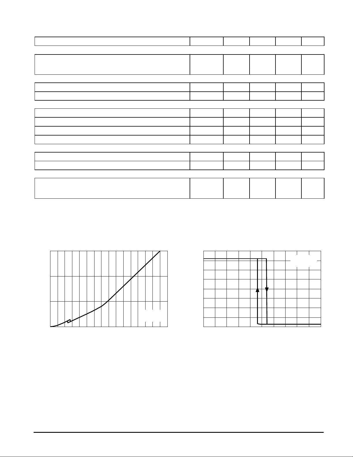
Figure 1. Input Current versus Input Voltage
1.5
1.0
0.5
, INPUT CURRENT (mA)
in
I
0
2.0 4.0 6.0 8.0 10 12 14 16
0
Vin, INPUT VOLTAGE (V)
VCC = 15 V
°
C
TA = 25
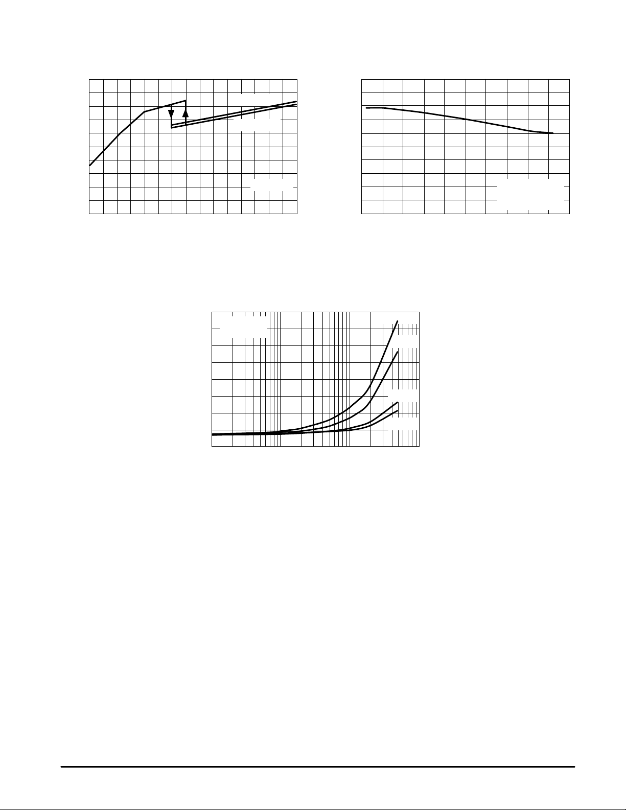
Figure 2. Output V oltage versus Input Voltage
16
14
12
10
8.0
6.0
, OUTPUT VOL TAGE (V)
4.0
O
V
2.0
0
0
1.0 2.0 3.0 4.0
Vin, INPUT VOLTAGE (V)
VCC = 15 V
°
C
TA = 25
5.0
MOTOROLA ANALOG IC DEVICE DATA
3
Page 4
MC33153
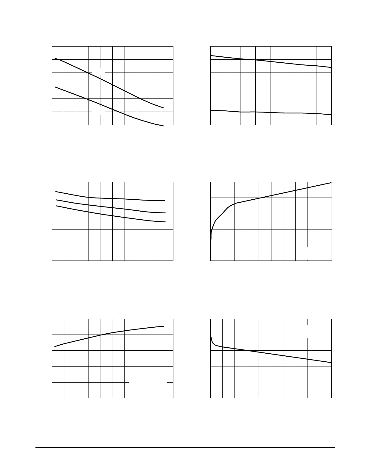
, INPUT THRESHOLD VOLTAGE (V)V
IL
– V
IH
Figure 3. Input Threshold V oltage
versus T emperature
3.2
3.0
2.8
2.6
2.4
2.2
2.0
–40 –20 0 20 40 60 80 100 120 140
–60
V
IH
V
IL
TA, AMBIENT TEMPERATURE (°C)
VCC = 15 V
Figure 5. Drive Output Low State Voltage
versus T emperature
2.5
2.0
1.5
I
= 1.0 A
Sink
= 500 mA
, INPUT THRESHOLD VOLTAGE (V)V
IL
– V
IH
Figure 4. Input Threshold V oltage
versus Supply V oltage
2.8
V
2.7
2.6
2.5
2.4
2.3
2.2
13 14 15 16 17 18 19 20
12
IH
V
IL
VCC, SUPPLY VOLTAGE (V)
Figure 6. Drive Output Low State Voltage
versus Sink Current
2.0
1.6
1.2
TA = 25°C
1.0
0.5
, OUTPUT LOW STATE VOLTAGE (V)
OL
V
0
–60
14.0
13.9
13.8
13.7
13.6
, DRIVE OUTPUT HIGH STATE VOLTAGE (V)
13.5
OH
–60
V
= 250 mA
VCC = 15 V
–40 –20 0 20 40 60 80 100 120 140
TA, AMBIENT TEMPERATURE (°C)
Figure 7. Drive Output High State Voltage
versus T emperature
VCC = 15 V
I
= 500 mA
Source
–40 –20 0 20 40 60 80 100 120 140
°
TA, AMBIENT TEMPERATURE (
C)
0.8
0.4
, OUTPUT LOW STATE VOLTAGE (V)
OL
V
0
0
15.0
14.6
14.2
13.8
13.4
, DRIVE OUTPUT HIGH STATE VOLTAGE (V)
13.0
OH
0
V
TA = 25°C
VCC = 15 V
0.2 0.4 0.6 0.8 1.0
I
, OUTPUT SINK CURRENT (A)
Sink
Figure 8. Drive Output High State Voltage
versus Source Current
VCC = 15 V
°
C
TA = 25
0.1 0.2 0.3 0.4 0.5
I
, OUTPUT SOURCE CURRENT (A)
Source
4
MOTOROLA ANALOG IC DEVICE DATA
Page 5

MC33153
Figure 9. Drive Output Voltage
versus Current Sense Input V oltage
16
14
12
10
8.0
6.0
4.0
, DRIVE OUTPUT VOLTAGE (V)
O
2.0
V
0
50
55 60 65 70 75 80
V
, CURRENT SENSE INPUT VOLTAGE (mV)
Pin 1
Figure 11. Overcurrent Protection Threshold
V oltage versus Temperature
70
68
VCC = 15 V
V
= 0 V
Pin 4
V
> 7.0 V
Pin 8
°
C
TA = 25
VCC = 15 V
Figure 10. Fault Output Voltage
versus Current Sense Input V oltage
14
12
10
8.0
6.0
4.0
, FAULT OUTPUT VOLTAGE (V)
2.0
Pin 7
V
0
100
110 120 130 140 150 160
V
, CURRENT SENSE INPUT VOLTAGE (mV)
Pin 1
Figure 12. Overcurrent Protection Threshold
V oltage versus Supply Voltage
70
68
VCC = 15 V
V
= 0 V
Pin 4
V
> 7.0 V
Pin 8
°
C
TA = 25
TA = 25°C
66
64
62
, OVERCURRENT THRESHOLD VOLTAGE (mV)
60
–40 –20 0 20 40 60 80 100 120 140
–60
SOC
V
TA, AMBIENT TEMPERATURE (°C)
Figure 13. Short Circuit Comparator Threshold
V oltage versus Temperature
135
130
VCC = 15 V
66
64
62
, OVERCURRENT THRESHOLD VOLTAGE (mV)
SOC
60
12
14 16 18 20
VCC, SUPPLY VOLTAGE (V)
Figure 14. Short Circuit Comparator Threshold
V oltage versus Supply Voltage
135
130
TA = 25°C
, SHORT CIRCUIT THRESHOLD VOLTAGE (mV)
125
SSC
V
–40 –20 0 20 40 60 80 100 120 140 14 16 18 20
–60
TA, AMBIENT TEMPERATURE (°C)
MOTOROLA ANALOG IC DEVICE DATA
, SHORT CIRCUIT THRESHOLD VOLTAGE (mV) V
SSC
V
125
12
VCC, SUPPLY VOLTAGE (V)
5
Page 6

MC33153
Figure 15. Current Sense Input Current
versus V oltage
0
µ
VCC = 15 V
°
C
TA = 25
–0.5
–1.0
, CURRENT SENSE INPUT CURRENT ( A)
SI
I
–1.5
0
4.0 6.0 8.0 10 12 14 162.0
V
, CURRENT SENSE INPUT VOLTAGE (V)
Pin 1
Figure 17. Fault Blanking/Desaturation Comparator
Threshold V oltage versus Temperature
6.6
VCC = 15 V
V
= 0 V
Pin 4
V
> 100 mV
Pin 1
Figure 16. Drive Output V oltage versus Fault
Blanking/Desaturation Input V oltage
16
14
12
10
8.0
6.0
4.0
, DRIVE OUTPUT VOLTAGE (V)
O
2.0
V
0
6.0
6.2 6.4 6.6 6.8 7.0
V
, FAULT BLANKING/DESATURATION INPUT VOLTAGE (V)
Pin 8
VCC = 15 V
V
= 0 V
Pin 4
V
> 100 mV
Pin 1
°
C
TA = 25
Figure 18. Fault Blanking/Desaturation Comparator
Threshold V oltage versus Supply Voltage
6.6
V
= 0 V
Pin 4
V
> 100 mV
Pin 1
°
C
TA = 25
THRESHOLD VOLTAGE (V)
, FAULT BLANKING/DESATURATION
BDT
V
µ
, CURRENT SOURCE ( A)
chg
I
6.5
6.4
–60
–20 0 20 40 60 80 100 120 140–40
TA, AMBIENT TEMPERATURE (°C)
Figure 19. Fault Blanking/Desaturation Current
Source versus T emperature
–200
–220
–240
–260
–280
VCC = 15 V
V
Pin 8
= 0 V
6.5
THRESHOLD VOLTAGE (V)
, FAULT BLANKING/DESATURATION
BDT
V
6.4
12
14 16 18 20
VCC, SUPPLY VOLTAGE (V)
Figure 20. Fault Blanking/Desaturation Current
Source versus Supply V oltage
–200
–220
µ
–240
–260
, CURRENT SOURCE ( A)I
–280
chg
V
Pin 4
V
Pin 8
TA = 25
= 0 V
= 0 V
°
C
–300
–60
–20 0 20 40 60 80 100 120 140–40 15 2010
TA, AMBIENT TEMPERATURE (°C)
6
–300
5.0
VCC, SUPPLY VOLTAGE (V)
MOTOROLA ANALOG IC DEVICE DATA
Page 7

MC33153
µ
, CURRENT SOURCE ( A)I
chg
Figure 21. Fault Blanking/Desaturation
Current Source versus Input Voltage
–200
–220
–240
–260
–280
–300
VCC = 15 V
V
= 0 V
Pin 4
°
C
TA = 25
0
V
Pin 8
4.0 6.0 8.0 10 12 14 162.0 4.0 8.0 12 16
, FAULT BLANKING/DESATURATION INPUT VOLTAGE (V)
Figure 23. Fault Output Low State Voltage
versus Sink Current
1.0
0.8
0.6
VCC = 15 V
V
= 5.0 V
Pin 4
°
C
TA = 25
Figure 22. Fault Blanking/Desaturation Discharge
Current versus Input Voltage
2.5
2.0
1.5
1.0
0.5
, DISCHARGE CURRENT (mA)I
dscg
–0.5
0
0
V
, FAULT BLANKING/DESATURATION INPUT VOLTAGE (V)
Pin 8
VCC = 15 V
V
Pin 4
TA = 25
Figure 24. Fault Output High State Voltage
versus Source Current
14.0
13.8
13.6
VCC = 15 V
V
Pin 4
V
Pin 1
Pin 8 = Open
TA = 25
= 5.0 V
°
C
= 0 V
= 1.0 V
°
C
0.4
, FAULT OUTPUT VOLTAGE (V)
0.2
Pin 7
V
0
0
16
14
12
10
8.0
6.0
4.0
, DRIVE OUTPUT VOLTAGE (V)
O
2.0
V
0
10
2.0 4.0 6.0 8.0 10
I
, OUTPUT SINK CURRENT (mA)
Sink
Figure 25. Drive Output Voltage
versus Supply V oltage
Turn–Off
Threshold
Startup
Threshold
11 12 13 14 15
VCC, SUPPLY VOLTAGE (V)
V
Pin 4
TA = 25
= 0 V
°
C
13.4
, FAULT OUTPUT VOLTAGE (V)
13.2
Pin 7
V
13.0
12.5
12.0
11.5
, UNDERVOL TAGE
11.0
th(UVLO)
LOCKOUT THRESHOLD (V)
V
10.5
–60
0
4.0 6.0 8.0 10 12 14 16 18 202.0
I
, OUTPUT SOURCE CURRENT (mA)
Source
Figure 26. UVLO Thresholds
versus T emperature
Startup Threshold
VCC Increasing
Turn–Off Threshold
VCC Decreasing
–20 20 60 100 140–40 0 40 80 120
TA, AMBIENT TEMPERATURE (°C)
MOTOROLA ANALOG IC DEVICE DATA
7
Page 8
10
Figure 27. Supply Current versus
Supply V oltage
MC33153
Figure 28. Supply Current versus T emperature
10
8.0
6.0
4.0
, SUPPLY CURRENT (mA)
2.0
CC
I
0
5.0
VCC, SUPPLY VOLTAGE (V)
Figure 29. Supply Current versus Input Frequency
80
VCC = 15 V
TA = 25
60
40
, SUPPLY CURRENT (mA)
20
CC
I
Output High
Output Low
TA = 25°C
°
C
8.0
6.0
4.0
, SUPPLY CURRENT (mA)
2.0
CC
I
0
–60
–4010 15
CL = 10 nF
= 5.0 nF
= 2.0 nF
= 1.0 nF
VCC = 15 V
V
Drive Output Open
0 20 40 60 80 100 120 14020 –20
TA, AMBIENT TEMPERATURE (
Pin 4
°
C)
= V
CC
0
1.0
f, INPUT FREQUENCY (kHz)
OPERA TING DESCRIPTION
GA TE DRIVE
Controlling Switching Times
The most important design aspect of an IGBT gate drive is
optimization of the switching characteristics. The switching
characteristics are especially important in motor control
applications in which PWM transistors are used in a bridge
configuration. In these applications, the gate drive circuit
components should be selected to optimize turn–on, turn–off
and off–state impedance. A single resistor may be used to
control both turn–on and turn–off as shown in Figure 30.
However, the resistor value selected must be a compromise
in turn–on abruptness and turn–off losses. Using a single
resistor is normally suitable only for very low frequency
PWM. An optimized gate drive output stage is shown in
Figure 31. This circuit allows turn–on and turn–off to be
optimized separately. The turn–on resistor, Ron, provides
control over the IGBT turn–on speed. In motor control
circuits, the resistor sets the turn–on di/dt that controls how
fast the free–wheel diode is cleared. The interaction of the
IGBT and free–wheeling diode determines the turn–on dv/dt.
Excessive turn–on dv/dt is a common problem in half–bridge
100010 100
circuits. The turn–off resistor, R
, controls the turn–off speed
off
and ensures that the IGBT remains off under commutation
stresses. Turn–off is critical to obtain low switching losses.
While IGBTs exhibit a fixed minimum loss due to minority
carrier recombination, a slow gate drive will dominate the
turn–off losses. This is particularly true for fast IGBTs. It is
also possible to turn–off an IGBT too fast. Excessive turn–off
speed will result in large overshoot voltages. Normally, the
turn–off resistor is a small fraction of the turn–on resistor.
The MC33153 contains a bipolar totem pole output stage
that is capable of sourcing 1.0 amp and sinking 2.0 amps
peak. This output also contains a pull down resistor to ensure
that the IGBT is off whenever there is insufficient VCC to the
MC33153.
In a PWM inverter, IGBTs are used in a half–bridge
configuration. Thus, at least one device is always off. While
the IGBT is in the off–state, it will be subjected to changes in
voltage caused by the other devices. This is particularly a
problem when the opposite transistor turns on.
8
MOTOROLA ANALOG IC DEVICE DATA
Page 9

MC33153
When the lower device is turned on, clearing the upper
diode, the turn–on dv/dt of the lower device appears across
the collector emitter of the upper device. To eliminate
shoot–through currents, it is necessary to provide a low sink
impedance to the device that is in the off–state. In most
applications the turn–off resistor can be made small enough
to hold off the device that is under commutation without
causing excessively fast turn–off speeds.
Figure 30. Using a Single Gate Resistor
and if desired, isolation from ac line voltages. An optoisolator
with a very high dv/dt capability should be used, such as the
Hewlett Packard HCPL4053. The IGBT gate turn–on resistor
should be set large enough to ensure that the opto’s dv/dt
capability is not exceeded. Like most optoisolators, the
HCPL4053 has an active low open–collector output. Thus,
when the LED is on, the output will be low. The MC33153 has
an inverting input pin to interface directly with an optoisolator
using a pull up resistor. The input may also be interfaced
directly to 5.0 V CMOS logic or a microcontroller.
V
CC
R
Output
5
V
V
EE
EE
3
V
EE
IGBT
g
Figure 31. Using Separate Resistors
for Turn–On and Turn–Off
V
CC
R
on
Output
5
V
V
EE
EE
3
V
EE
R
D
off
off
IGBT
Optoisolator Output Fault
The MC33153 has an active high fault output. The fault
output may be easily interfaced to an optoisolator. While it is
important that all faults are properly reported, it is equally
important that no false signals are propagated. Again, a high
dv/dt optoisolator should be used.
The LED drive provides a resistor programmable current
of 10 to 20 mA when on, and provides a low impedance path
when off. An active high output, resistor, and small signal
diode provide an excellent LED driver. This circuit is shown in
Figure 32.
Figure 32. Output Fault Optoisolator
Short Circuit
Latch Output
V
CC
Q
7
V
V
EE
EE
A negative bias voltage can be used to drive the IGBT into
the off–state. This is a practice carried over from bipolar
Darlington drives and is generally not required for IGBTs.
However, a negative bias will reduce the possibility of
shoot–through. The MC33153 has separate pins for VEE and
Kelvin Ground. This permits operation using a +15/–5.0 V
supply.
INTERFACING WITH OPTOISOLATORS
Isolated Input
The MC33153 may be used with an optically isolated
input. The optoisolator can be used to provide level shifting,
UNDERVOLTAGE LOCKOUT
It is desirable to protect an IGBT from insufficient gate
voltage. IGBTs require 15 V on the gate to achieve the rated
on–voltage. At gate voltages below 13 V, the on–voltage
increases dramatically, especially at higher currents. At very
low gate voltages, below 10 V, the IGBT may operate in the
linear region and quickly overheat. Many PWM motor drives
use a bootstrap supply for the upper gate drive. The UVLO
provides protection for the IGBT in case the bootstrap
capacitor discharges.
The MC33153 will typically start up at about 12 V. The
UVLO circuit has about 1.0 V of hysteresis and will disable
the output if the supply voltage falls below about 1 1 V.
MOTOROLA ANALOG IC DEVICE DATA
9
Page 10

MC33153
PROTECTION CIRCUITRY
Desaturation Protection
Bipolar Power circuits have commonly used what is known
as “Desaturation Detection”. This involves monitoring the
collector voltage and turning off the device if this voltage rises
above a certain limit. A bipolar transistor will only conduct a
certain amount of current for a given base drive. When the
base is overdriven, the device is in saturation. When the
collector current rises above the knee, the device pulls out of
saturation. The maximum current the device will conduct in
the linear region is a function of the base current and the dc
current gain (hFE) of the transistor.
The output characteristics of an IGBT are similar to a
Bipolar device. However, the output current is a function of
gate voltage instead of current. The maximum current
depends on the gate voltage and the device type. IGBT s tend
to have a very high transconductance and a much higher
current density under a short circuit than a bipolar device.
Motor control IGBTs are designed for a lower current density
under shorted conditions and a longer short circuit survival
time.
The best method for detecting desaturation is the use of a
high voltage clamp diode and a comparator. The MC33153
has a Fault Blanking/Desaturation Comparator which senses
the collector voltage and provides an output indicating when
the device is not fully saturated. Diode D1 is an external high
voltage diode with a rated voltage comparable to the power
device. When the IGBT is “on” and saturated, D1 will pull
down the voltage on the Fault Blanking/Desaturation Input.
When the IGBT pulls out of saturation or is “off”, the current
source will pull up the input and trip the comparator. The
comparator threshold is 6.5 V, allowing a maximum
on–voltage of about 5.8 V.
A fault exists when the gate input is high and VCE is
greater than the maximum allowable V
CE(sat)
the Desaturation Comparator is ANDed with the gate input
signal and fed into the Short Circuit and Overcurrent Latches.
The Overcurrent Latch will turn–off the IGBT for the
remainder of the cycle when a fault is detected. When input
goes high, both latches are reset. The reference voltage is
tied to the Kelvin Ground instead of the VEE to make the
threshold independent of negative gate bias. Note that for
proper operation of the Desaturation Comparator and the
Fault Output, the Current Sense Input must be biased above
the Overcurrent and Short Circuit Comparator thresholds.
This can be accomplished by connecting Pin 1 to VCC.
Figure 33. Desaturation Detection
V
Kelvin
Gnd
CC
V
ref
6.5 V
270
V
CC
µ
A
8
V
EE
Desaturation
Comparator
. The output of
D1
The MC33153 also features a programmable fault
blanking time. During turn–on, the IGBT must clear the
opposing free–wheeling diode. The collector voltage will
remain high until the diode is cleared. Once the diode has
been cleared, the voltage will come down quickly to the
V
considerable ringing on the collector due to the C
of the device. Following turn–on, there is normally
CE(sat)
OSS
capacitance of the IGBT s and the parasitic wiring inductance.
The fault signal from the Desaturation Comparator must be
blanked sufficiently to allow the diode to be cleared and the
ringing to settle out.
The blanking function uses an NPN transistor to clamp the
comparator input when the gate input is low. When the input
is switched high, the clamp transistor will turn “off”, allowing
the internal current source to charge the blanking capacitor.
The time required for the blanking capacitor to charge up
from the on–voltage of the internal NPN transistor to the trip
voltage of the comparator is the blanking time.
If a short circuit occurs after the IGBT is turned on and
saturated, the delay time will be the time required for the
current source to charge up the blanking capacitor from the
V
level of the IGBT to the trip voltage of the
CE(sat)
comparator. Fault blanking can be disabled by leaving Pin 8
unconnected.
Sense IGBT Protection
Another approach to protecting the IGBTs is to sense the
emitter current using a current shunt or Sense IGBTs. This
method has the advantage of being able to use high gain
IGBTs which do not have any inherent short circuit capability.
Current sense IGBTs work as well as current sense
MOSFETs in most circumstances. However, the basic
problem of working with very low sense voltages still exists.
Sense IGBTs sense current through the channel and are
therefore linear with respect to the collector current. Because
IGBTs have a very low incremental on–resistance, sense
IGBTs behave much like low–on resistance current sense
MOSFETs. The output voltage of a properly terminated
sense IGBT is very low, normally less than 100 mV.
The sense IGBT approach requires fault blanking to
prevent false tripping during turn–on. The sense IGBT also
requires that the sense signal is ignored while the gate is low.
This is because the mirror output normally produces large
transient voltages during both turn–on and turn–off due to the
collector to mirror capacitance. With non–sensing types of
IGBTs, a low resistance current shunt (5.0 to 50 mΩ) can be
used to sense the emitter current. When the output is an
actual short circuit, the inductance will be very low. Since the
blanking circuit provides a fixed minimum on–time, the peak
current under a short circuit can be very high. A short circuit
discern function is implemented by the second comparator
which has a higher trip voltage. The short circuit signal is
latched and appears at the Fault Output. When a short circuit
is detected, the IGBT should be turned–off for several
milliseconds allowing it to cool down before it is turned back
on. The sense circuit is very similar to the desaturation
circuit. It is possible to build a combination circuit that
provides protection for both Short Circuit capable IGBTs and
Sense IGBTs.
10
MOTOROLA ANALOG IC DEVICE DATA
Page 11

MC33153
APPLICATION INFORMATION
Figure 34 shows a basic IGBT driver application. When
driven from an optoisolator, an input pull up resistor is
required. This resistor value should be set to bias the output
transistor at the desired current. A decoupling capacitor
should be placed close to the IC to minimize switching noise.
A bootstrap diode may be used for a floating supply . If the
protection features are not required, then both the Fault
Blanking/Desaturation and Current Sense Inputs should both
be connected to the Kelvin Ground (Pin 2). When used with a
single supply, the Kelvin Ground and VEE pins should be
connected together. Separate gate resistors are
recommended to optimize the turn–on and turn–off drive.
Figure 34. Basic Application
18 V
B+
7
4
Fault
MC33153
Input
Bootstrap
6
V
CC
V
EE
3
Desat/
Blank
Output
Sense
Gnd
8
5
1
2
If desaturation protection is desired, a high voltage diode
is connected to the Fault Blanking/Desaturation pin. The
blanking capacitor should be connected from the
Desaturation pin to the VEE pin. If a dual supply is used, the
blanking capacitor should be connected to the Kelvin
Ground. The Current Sense Input should be tied high
because the two comparator outputs are ANDed together.
Although the reverse voltage on collector of the IGBT is
clamped to the emitter by the free–wheeling diode, there is
normally considerable inductance within the package itself. A
small resistor in series with the diode can be used to protect
the IC from reverse voltage transients.
Figure 36. Desaturation Application
18 V
7
4
Fault
Input
6
V
CC
MC33153
V
EE
3
Desat/
Blank
Output
Sense
Gnd
8
C
Blank
5
1
2
Figure 35. Dual Supply Application
15 V
6
7
Fault
V
CC
Desat/
Blank
Output
8
5
MC33153
4
–5.0 V
Input
V
EE
3
Sense
Gnd
1
2
When used in a dual supply application as in Figure 35, the
Kelvin Ground should be connected to the emitter of the
IGBT. If the protection features are not used, then both the
Fault Blanking/Desaturation and the Current Sense Inputs
should be connected to Ground. The input optoisolator
should always be referenced to VEE.
When using sense IGBTs or a sense resistor, the sense
voltage is applied to the Current Sense Input. The sense trip
voltages are referenced to the Kelvin Ground pin. The sense
voltage is very small, typically about 65 mV, and sensitive to
noise. Therefore, the sense and ground return conductors
should be routed as a differential pair . An RC filter is useful in
filtering any high frequency noise. A blanking capacitor is
connected from the blanking pin to VEE. The stray
capacitance on the blanking pin provides a very small level of
blanking if left open. The blanking pin should not be grounded
when using current sensing, that would disable the sense.
The blanking pin should never be tied high, that would short
out the clamp transistor.
Figure 37. Sense IGBT Application
18 V
7
Fault
4
Input
6
V
CC
MC33153
V
EE
3
Desat/
Blank
Output
Sense
Gnd
8
5
1
2
MOTOROLA ANALOG IC DEVICE DATA
11
Page 12

MC33153
OUTLINE DIMENSIONS
P SUFFIX
PLASTIC PACKAGE
CASE 626–05
58
ISSUE K
NOTE 2
C
–T–
SEATING
PLANE
H
A
E
B
A1
14
F
–A–
N
D
G
0.13 (0.005) B
D
58
0.25MB
1
H
4
e
A
B
SS
A0.25MCB
–B–
C
SEATING
PLANE
K
M
A
T
PLASTIC PACKAGE
M
0.10
L
J
M
M
M
D SUFFIX
CASE 751–06
(SO–8)
ISSUE T
h
X 45
_
NOTES:
1. DIMENSION L TO CENTER OF LEAD WHEN
FORMED PARALLEL.
2. PACKAGE CONTOUR OPTIONAL (ROUND OR
SQUARE CORNERS).
3. DIMENSIONING AND TOLERANCING PER ANSI
Y14.5M, 1982.
DIM MIN MAX MIN MAX
A 9.40 10.16 0.370 0.400
B 6.10 6.60 0.240 0.260
C 3.94 4.45 0.155 0.175
D 0.38 0.51 0.015 0.020
F 1.02 1.78 0.040 0.070
G 2.54 BSC 0.100 BSC
H 0.76 1.27 0.030 0.050
J 0.20 0.30 0.008 0.012
K 2.92 3.43 0.115 0.135
L 7.62 BSC 0.300 BSC
M ––– 10 ––– 10
N 0.76 1.01 0.030 0.040
NOTES:
1. DIMENSIONING AND TOLERANCING PER ASME
Y14.5M, 1994.
2. DIMENSIONS ARE IN MILLIMETER.
C
q
3. DIMENSION D AND E DO NOT INCLUDE MOLD
PROTRUSION.
4. MAXIMUM MOLD PROTRUSION 0.15 PER SIDE.
5. DIMENSION B DOES NOT INCLUDE DAMBAR
PROTRUSION. ALLOWABLE DAMBAR
PROTRUSION SHALL BE 0.127 TOTAL IN EXCESS
OF THE B DIMENSION AT MAXIMUM MATERIAL
CONDITION.
DIM MIN MAX
A 1.35 1.75
A1 0.10 0.25
B 0.35 0.49
C 0.19 0.25
D 4.80 5.00
E
H 5.80 6.20
L
h
L 0.40 1.25
q
INCHESMILLIMETERS
__
MILLIMETERS
3.80 4.00
1.27 BSCe
0.25 0.50
0 7
__
Motorola reserves the right to make changes without further notice to any products herein. Motorola makes no warranty , representation or guarantee regarding
the suitability of its products for any particular purpose, nor does Motorola assume any liability arising out of the application or use of any product or circuit, and
specifically disclaims any and all liability, including without limitation consequential or incidental damages. “T ypical” parameters which may be provided in Motorola
data sheets and/or specifications can and do vary in different applications and actual performance may vary over time. All operating parameters, including “Typicals”
must be validated for each customer application by customer’s technical experts. Motorola does not convey any license under its patent rights nor the rights of
others. Motorola products are not designed, intended, or authorized for use as components in systems intended for surgical implant into the body, or other
applications intended to support or sustain life, or for any other application in which the failure of the Motorola product could create a situation where personal injury
or death may occur. Should Buyer purchase or use Motorola products for any such unintended or unauthorized application, Buyer shall indemnify and hold Motorola
and its officers, employees, subsidiaries, affiliates, and distributors harmless against all claims, costs, damages, and expenses, and reasonable attorney fees
arising out of, directly or indirectly, any claim of personal injury or death associated with such unintended or unauthorized use, even if such claim alleges that
Motorola was negligent regarding the design or manufacture of the part. Motorola and are registered trademarks of Motorola, Inc. Motorola, Inc. is an Equal
Opportunity/Affirmative Action Employer.
Mfax is a trademark of Motorola, Inc.
How to reach us:
USA/EUROPE/Locations Not Listed: Motorola Literature Distribution; JAPAN: Nippon Motorola Ltd.: SPD, Strategic Planning Office, 141,
P.O. Box 5405, Denver, Colorado 80217. 1–303–675–2140 or 1–800–441–2447 4–32–1 Nishi–Gotanda, Shagawa–ku, Tokyo, Japan. 03–5487–8488
Customer Focus Center: 1–800–521–6274
Mfax: RMFAX0@email.sps.mot.com – TOUCHTONE 1–602–244–6609 ASIA/PACIFIC: Motorola Semiconductors H.K. Ltd.; 8B Tai Ping Industrial Park,
Moto rola Fax Back Sys tem – US & Canada ONLY 1–800–774–1848 51 Ting Kok Road, Tai Po, N.T., Hong Kong. 852–26629298
– http://sps.motorola.com/mfax/
HOME PAGE: http://motorola.com/sps/
12
◊
MOTOROLA ANALOG IC DEVICE DATA
MC33153/D
 Loading...