

Page 1
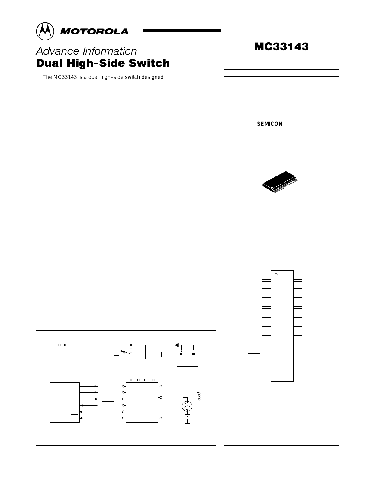
Order this document by MC33143/D
The MC33143 is a dual high–side switch designed for solenoid control in
harsh automotive applications, but is well suited for other environments. The
device can also be used to control small motors and relays as well as
solenoids. The MC33143 incorporates SMARTMOS technology, with
CMOS logic, bipolar/MOS analog circuitry, and DMOS power outputs. An
internal charge pump is incorporated for efficient gate enhancement of the
internal high–side power output devices. The outputs are designed to
provide current to low impedance solenoids. The MC33143 provides
individual output fault status reporting along with internal Overcurrent and
Over Temperature protection. The device also has Overvoltage protection,
with automatic recovery, which “globally” disables both outputs for the
duration of an Overvoltage condition. Each output has individual Overcurrent
and Over Temperature shutdown with automatic retry recovery. Outputs are
enabled with a CMOS logic high signal applied to an input to providing true
logic control. The outputs, when turned on, provide full supply (battery)
voltage across the solenoid coil.
The MC33143 is packaged in an economical 24 pin surface mount power
package and specified over an operating voltage of 5.5 V ≤ V
–40°C ≤ TA ≤ 125°C.
• Designed to Operate Over Wide Supply Voltages of 5.5 V to 26 V
• Dual High–Side Outputs Clamped to –10 V for Driving Inductive Loads
• Internal Charge Pump for Enhanced Gate Drive
• Interfaces Directly to a Microcontroller with Parallel Input Control
• Outputs Current Limited to 3.0 A to 6.0 A for Driving Incandescent Loads
• Chip Enable “Sleep Mode” for Power Conservation
• Individual Output Status Reporting
• Fault Interrupt Output for System Interrupt Use
• Output ON or OFF Open Load Detection
• Overvoltage Detection and Shutdown
• Output Over Temperature Detection and Shutdown with Automatic Retry
• Sustained Current Limit or Immediate Overcurrent Shutdown Output Modes
• Output Short to Ground Detection and Shutdown with Automatic Retry
• Output Short to V
SMARTMOS is a trademark of Motorola, Inc.
V
DD
V
P0
DD
P1
P2
MCU
P3
P4
IRQ
NOTE: Pins 5, 6, 7, 8, 17, 18, 19 and 20 provide electrical ground and heatsinking.
This document contains information on a new product. Specifications and information herein
are subject to change without notice.
MOTOROLA ANALOG IC DEVICE DATA
Detection
Pwr
Simplified Application
+V
Pwr
(16)
(11)
Pwr
DD
SFPD (14)
CEN (2)
IN1 (1)
IN2 (12)
STAT1
(13)
STAT2 (10)
INT (23)
This device contains 889 active transistors.
MC33143
GTST (15)
V
V
OUT1 (24)
OUT2 (13)
Gnd (Note)
< 26 V for
Pwr
Battery
DUAL HIGH–SIDE
SWITCH
SEMICONDUCTOR
TECHNICAL DATA
24
1
DW SUFFIX
PLASTIC PACKAGE
CASE 751E
(SOP (16+4+4)L)
PIN CONNECTIONS
23
22
21
20
19
18
17
16
15
14
13
OUT1
INT
N/C
V
Pwr
Gnd
Gnd
Gnd
Gnd
V
Pwr
GTST
SFPD
OUT2
Package
SOP–24L
1
124
IN1
CEN
2
STAT1
3
4
V
Pwr
Gnd
5
Gnd
6
Gnd
7
Gnd
8
9
V
Pwr
10
STAT2
V
11
DD
IN2
12
(Top View)
ORDERING INFORMATION
Operating
Device
MC33143DW TA = – 40° to +125°C
Motorola, Inc. 1996 Rev 0
Temperature Range
Page 2
V
(9, 16)
Pwr
SFPD (14)
IN1 (1)
VDD (11)
GTST (15)
CEN (2)
IN2 (12)
Gnd (5) (See Note)
NOTE: Pins 5, 6, 7, 8, 17, 18, 19 and 20 should all be grounded so as to provide electrical as well as thermal heatsinking of the device.
Overvoltage
Shutdown
Bias
Charge
Pump
MC33143
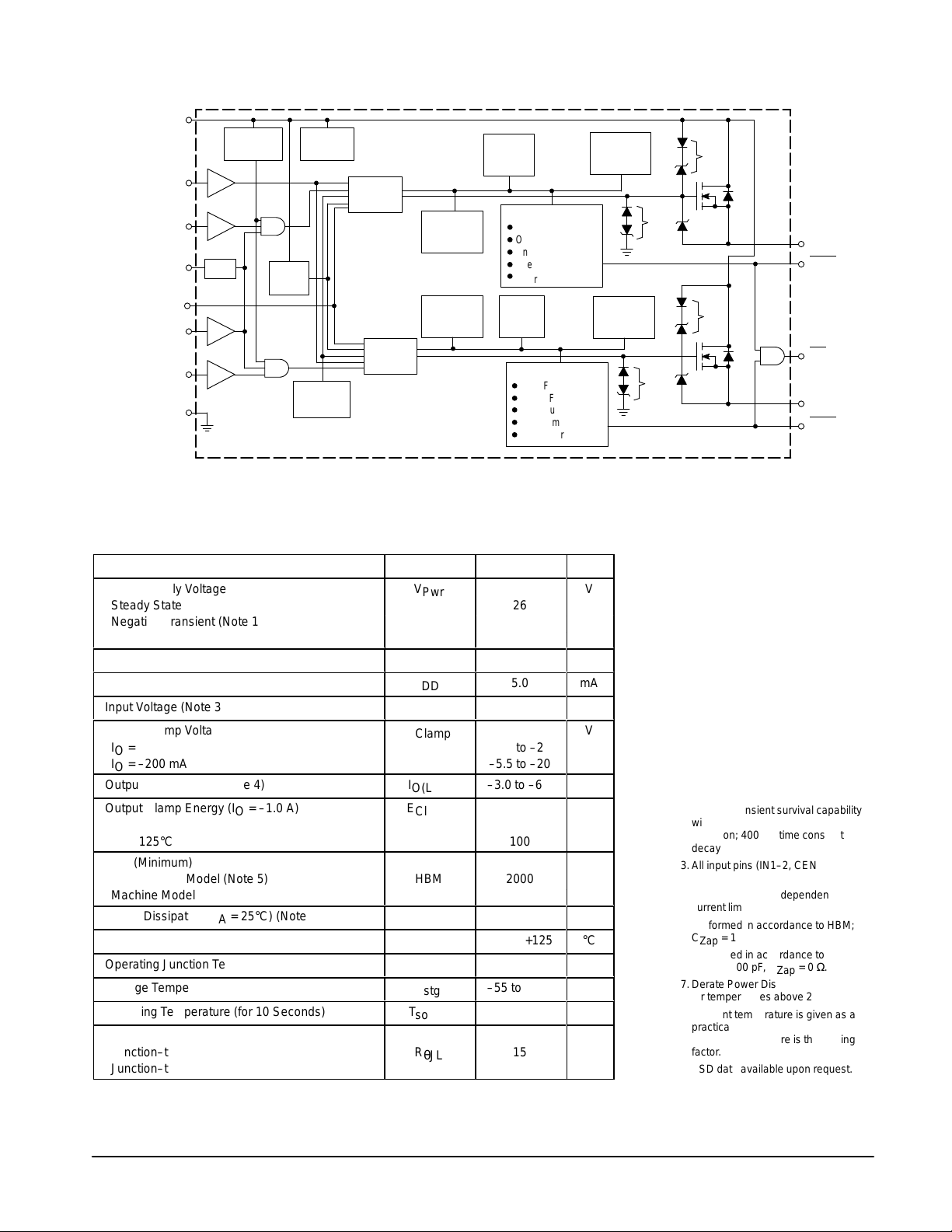
Figure 1. Simplified Internal Block Diagram
Voltage
Regulator
4.0 ms
Retry Timer
Gate
Control
Gate
Control
OFF/ON
Open Load
Detect
OFF/ON
Open Load
Detect
Current
Limit
Fault Detection
D
ON/OFF Open Load
D
ON/OFF V
D
On Ground Short
D
Over Temperature
D
V
Pwr
Current
Limit
Fault Detection
D
ON/OFF Open Load
D
ON/OFF V
D
On Ground Short
D
Over Temperature
D
V
Pwr
Short
Pwr
Overvoltage
Short
Pwr
Overvoltage
Over
T emperature
Shutdown
Over
T emperature
Shutdown
–10 V
–10 V
15 V
15 V
55 V
55 V
OUT1 (24)
(3)
STAT1
INT
(23)
OUT2 (13)
(10)
STAT2
MAXIMUM RATINGS (All voltages are with respect to ground, unless otherwise noted.)
Rating Symbol Value Unit
Power Supply Voltage
Steady State Continuous Operation 26
Negative Transient (Note 1) –1.5
Positive Load Dump Transient (Note 2) 60
Logic Supply Voltage Range
Logic Supply Current
Input Voltage (Note 3)
Output Clamp Voltage
IO = –20 mA –3.0 to –20
IO = –200 mA –5.5 to –20
Output Current Limit (Note 4)
Output Clamp Energy (IO = –1.0 A)
TJ = 25°C 300
TJ = 125°C 100
ESD (Minimum) V
Human Body Model (Note 5) HBM 2000
Machine Model (Note 6) MM 200
Power Dissipation (TA = 25°C) (Note 7)
Operating Temperature (Note 8)
Operating Junction Temperature
Storage Temperature
Soldering Temperature (for 10 Seconds)
Thermal Resistance
Junction–to–Lead R
Junction–to–Ambient R
V
Pwr
V
DD
I
DD
V
V
Clamp
I
O(Lim)
E
Clamp
P
T
T
T
stg
T
solder
θJL
θJA
–0.3 to 7.0
5.0
in
–0.3 to 7.0
–3.0 to –6.0
D
A
J
4.2
–40 to +125
–40 to +150
–55 to +150
270
°C/W
15
30
V
V
mA
V
V
A
mJ
W
°C
°C
°C
°C
NOTES: 1. Negative transient survival capability
for 100 ms time duration.
2.Positive transient survival capability
with typical automotive load dump
condition; 400 ms time constant
decay.
3.All input pins (IN1–2, CEN and
SFPD).
4.Each output has independent
current limiting.
5.Performed in accordance to HBM;
C
= 100 pF, R
Zap
6.Performed in accordance to MM;
C
= 100 pF, R
Zap
7.Derate Power Dissipation 33 mW/°C
for temperatures above 25°C.
8.Ambient temperature is given as a
practical reference; Maximum
junction temperature is the limiting
factor.
9.ESD data available upon request.
= 1500 Ω.
Zap
= 0 Ω.
Zap
2
MOTOROLA ANALOG IC DEVICE DATA
Page 3

MC33143
ÁÁÁ
ÁÁÁ
Á
Á
Á
Á
Á
ÁÁÁ
Á
ÁÁÁ
ÁÁÁ
ÁÁÁ
ÁÁÁ
ÁÁÁ
ÁÁÁ
ÁÁÁ
ÁÁÁ
ÁÁÁ
ÁÁÁ
ÁÁÁ
DC ELECTRICAL CHARACTERISTICS (Characteristics noted under conditions 9.0 V ≤ V
≤ 17 V, 4.5 V ≤ VDD 5.5 V,
Pwr
–40°C ≤ TL ≤ 125°C, unless otherwise noted, typical values represent approximate mean at TL = 25°C.)
Characteristic
Symbol Min Typ Max Unit
POWER INPUT
Supply Voltage Range (Operational)
V
Pwr
9.0
–
17
Supply Current (Note 1)
Both Outputs ON
(CEN = IN1 = IN2 = 0.7 x VDD, IO1 = IO2 = –1.0 A) I
Standby (CEN = 0.7 x VDD, IN1 = IN2 = 0.3 x VDD, RL = 12 Ω) I
“Sleep State” (CEN = IN1 = IN2 = 0.3 x VDD, RL = 12 Ω) I
Logic Supply Voltage Range
БББББББББББББББББ
Logic Supply Current
Pwr
Pwr(sby)
Pwr(sleep)
V
DD
ÁÁÁ
I
DD
0.1 4.2 7.0 mA
– 3.9 7.0 mA
– 0.2 300 µA
4.5
ÁÁ
–
–
ÁÁ
0.43
5.5
ÁÁ
5.0
Both Outputs ON (IN1 = IN2 = 0.7 x VDD, IO1 = IO2 = –1.0 A) mA
Overvoltage Shutdown (Note 2)
Overvoltage Shutdown Hysteresis
NOTES: 1. Supply current when both outputs are ON and during standby are measured in the Ground pin while during “sleep state” is measured in the V
2.Overvoltage Shutdown causes enabled outputs to be forced OFF; Overvoltage fault is immediately reported.
DC ELECTRICAL CHARACTERISTICS (Characteristics noted under conditions 9.0 V ≤ V
V
Pwr(ovsd)
V
Pwr(hys)
30
0.3
≤ 17 V, 4.5 V ≤ VDD 5.5 V,
Pwr
33.2
0.5
38
1.5
–40°C ≤ TL ≤ 125°C, unless otherwise noted, typical values represent approximate mean at TL = 25°C.)
Characteristic
Symbol Min Typ Max Unit
POWER OUTPUT
Drain–to–Source ON Resistance (Note 1)
R
DS(on)
(TJ = 25°C, CEN = IN1 = IN2 = 0.7 x VDD)
IO = –0.5 A. V
IO = –1.0 A. V
IO = –2.0 A. V
Drain–to–Source ON Resistance (Note 1)
= 5.5 V – 0.2 0.5
Pwr
= 14 V – 0.14 0.2
Pwr
= 24 V – 0.14 0.2
Pwr
R
DS(on)
(TJ = 125°C, CEN = IN1 = IN2 = 0.7 x VDD)
IO = –0.5 A. V
IO = –1.0 A. V
IO = –2.0 A. V
Output Self–Limiting Current (Note 2)
= 5.5 V – – 1.0
Pwr
= 14 V – – 0.38
Pwr
= 24 V – – 0.38
Pwr
I
O(Lim)
–3.0
–4.1
–6.0
(CEN = IN1 = IN2 = SFPD = 0.7 x VDD, RL = 0 Ω)
Output OFF Leakage Current
I
O(Lkg)
–5.0
–45
–150
(CEN = 0.7 x VDD, IN1 = IN2 = 0.3 x VDD)
Output OFF Open Load Sense Current
I
O(Sense)
–5.0
–45
–150
(CEN = 0.7 x VDD, IN1 = IN2 = 0.3 x VDD)
Output ON Open Load Detection Current (Note 3)
I
O(On)
(CEN = IN1 = IN2 = 0.7 x VDD)
TL = –40°C –2.0 –145 –200
TL = 125°C –2.0 –181 –200
Output Clamp Voltage (Note 4)
V
Clamp
(CEN = 0.7 x VDD, IN1 = IN2 = 0.3 x VDD)
IO = –20 mA –9.0 –13.2 –20
IO = –200 mA –9.0 –13.5 –20
Over T emperature Shutdown Range (Note 5)
T
Lim
155
–
185
(CEN = IN1 = IN2 = SFPD = 0.7 x VDD)
Over Temperature Shutdown Hysteresis (Note 6)
NOTES: 1. R
2.Applies to each output; each output has independent self–limiting source current feature; Over Current and Short–to–Ground defined as condition
3.Applies to each output; tested for by ramping IO from 0 until STAT
4.Applies to each output; each output has independent dynamic output voltage clamping feature.
5.Applies to each output; each output has independent thermal shutdown; parameter is measured by ramping temperature until enabled output is
6.Parameter is established by design but is not production tested.
applies to OUT1, OUT2 and is independent of output current.
DS(on)
when output source current exceeds I
; Device ignores Over Current and Short–to–Ground faults from 0 to tss.
O(Lim)
≤ 0.7 x VDD; defined as the condition when IO is outside of I
disabled; parameter is established by design but is not production tested; thermal fault is immediately reported.
T
Lim(hys)
–
–
15
current window.
O(on)
V
V
ÁÁ
V
V
pin.
Pwr
Ω
Ω
A
µA
µA
mA
V
°C
°C
MOTOROLA ANALOG IC DEVICE DATA
3
Page 4

MC33143
ÁÁÁ
ÁÁÁ
ÁÁÁ
ÁÁÁ
ÁÁÁ
ÁÁÁ
ÁÁÁ
ÁÁÁ
ÁÁÁ
ÁÁÁ
ÁÁÁ
ÁÁÁ
ÁÁÁ
DC ELECTRICAL CHARACTERISTICS
(Characteristics noted under conditions 9.0 V ≤ V
≤ 17 V, 4.5 V ≤ VDD 5.5 V,
Pwr
–40°C ≤ TL ≤ 125°C, unless otherwise noted, typical values represent approximate mean at TL = 25°C.)
Characteristic
Symbol Min Typ Max Unit
CONTROL INTERFACE
Input Control
Logic High (IO = –0.1 A) (Note 1) V
Logic Low (IO = 0) (Note 2) V
Input Logic Voltage Hysteresis (VIH – VIL)
Input Pull–Down Current (0.3 x VDD ≤ Vin < 0.7 x VDD) (Note 3)
IH
V
hys
I
in(pd)
IL
0.7 0.56 –
– 0.52 0.3
50
20
Chip–Enable Threshold
Logic Low (Note 4) V
Logic High (Note 5) V
Chip–Enable Hysteresis (V
CEN(IH)
– V
CEN(IL)
)
Chip–Enable Pull–Up Current (CEN = 0.7 x VDD)
Status Low Voltage (Iin = 600 µA) (Note 6)
Status Pull–Up Current (Note 7)
CEN(IL)
CEN(IH)
V
CEN(hys)
I
CEN(pu)
V
STAT
I
STAT(pu)
(low)
– 0.5 0.3
0.7 0.5 –
50
–2.0
–
–20
Interrupt (Note 8)
Logic High INT
Logic Low INT
NOTES: 1. Upper logic threshold voltage applies to IN1, IN2, and SFPD and expressed in VDD units
2.Lower logic threshold voltage applies to IN1, IN2, and SFPD and expressed in VDD units.
3.Applies to IN1, IN2, and SFPD.
4.Initially have CEN = 0.7 x VDD, Ramp CEN down from VDD until IO = 0 and note disabling point.
5.Initially have Vin = 0.7 x VDD, Ramp CEN up from ground until IO = 0.1 A and note enabling point.
6.Applies equally to STAT1–2
current into STAT1–2
7.Measured with no faults on OUT1–2, V
8. The Interrupt output has an internal active current pull–up
and INT outputs; Measured threshold voltage by applying an “open” fault to OUT1 or OUT2 while forcing 600 µA of
or INT.
= V
STAT
= 0.8 x VDD.
INT
.
h
l
0.7 – –
– – 0.3
250
44
150
–16.8
0.07
–44
500
100
500
–40
0.2
–100
V
V
V
V
DD
mV
µA
DD
mV
µA
DD
µA
DD
DC ELECTRICAL CHARACTERISTICS (Characteristics noted under conditions 9.0 V ≤ V
≤ 17 V, 4.5 V ≤ VDD 5.5 V,
Pwr
–40°C ≤ TL ≤ 125°C, unless otherwise noted, typical values represent approximate mean at TL = 25°C.)
Characteristic
Symbol Min Typ Max Unit
OUTPUT DYNAMICS
Output Short Sense Time (Note 1)
Output Short Refresh Time (Note 2)
Output Open Sense ON Time (Note 3)
t
ss
t
ref
t
os(on)
30
3.0
3.0
54
4.1
6.4
100
6.0
12
Output Propagation Delay
Turn–On (Output Low to High) (Note 4) t
Turn–Off (Output High to Low) (Note 5) t
dlh
dhl
– 7.2 50
– 40 75
Output Slew Rate
Output Rising (Note 6) SR
Output Falling (Note 7) SR
NOTES: 1. CEN = 0.7 x VDD, SFPD = 0.3 x VDD, RL = 0, Step Vin from 0.3 x VDD to 0.7 x VDD; Sense time measured from step until STAT = 0.2 x VDD.
2.CEN = IN1 = IN2 = 0.7 x VDD, RL = 0; Refresh time measured from output disable until output is re–enabled.
3.RL = “open”, Step Vin from ground to 0.7 x VDD, Open sense time measured from step until V
4.RL = 12 Ω, CL = 0.01 µF, step Vin from VIL to VIH; Turn–On propagation measured from Vin = 0.5 x VDD until V
5.RL = 12 Ω, CL = 0.01 µF, step Vin from VIH to VIL; Turn–Off propagation measured from V
6.RL = 12 Ω, CL = 0.01 µF, step Vin from VIL to VIH; Output Slew Rate measured from 2.0 V to V
7.RL = 12 Ω, CL = 0.01 µF, step Vin from VIH to VIL; Output Slew Rate measured from V
r
f
Pwr
0.2 11 10
0.2 2.6 10
≤ 0.2 x VDD.
STAT
= V
out
– 3.0 V to 2.0 V (see Figure 2).
–3.0 V until V
Pwr
– 3.0 V (see Figure 2).
Pwr
= 2.0 V (see Figure 2).
out
= 2.0 V (see Figure 2).
out
µs
ms
ms
µs
V/µs
4
MOTOROLA ANALOG IC DEVICE DATA
Page 5

MC33143
Á
Á
Á
Á
Á
Á
Á
Á
Á
Á
Á
Á
Á
Á
Á
Á
Á
Á
Á
Á
Á
Á
Á
Á
Figure 2. Output Response Waveform
5.0 V
IN1–2
50%
0 V
V
Pwr
t
dlh
V
– 3.0 V
Pwr
t
dhl
OUT1–2
t
SRr
2.0 V
t
SRf
0 V
PIN FUNCTION DESCRIPTION
Pin Symbol Description
1, 12
ÁÁ
ÁÁ
2 CEN Chip Enable (CEN) input pin, when low, disables both outputs (OUT1 and OUT2) and places the device
3, 10 STAT1. STAT2 The STATus pins (STAT1–2) respectively indicate the presence of faults on OUT1–2. STAT1–2 will be
4, 9, 16,21V
5, 6, 7, 8,
17, 18,
ÁÁ
19, 20
11
ÁÁ
13, 24
ÁÁ
ÁÁ
ÁÁ
ÁÁ
IN1, IN2
ÁÁÁÁ
ÁÁÁÁ
Pwr
Gnd
ÁÁÁÁ
V
DD
ÁÁÁÁ
OUT1, OUT2
ÁÁÁÁ
ÁÁÁÁ
ÁÁÁÁ
ÁÁÁÁ
INput 1 and INput 2 (IN1 and IN2) respectively determine the state of the corresponding output drivers
(OUT1 and OUT2) under normal operating conditions. When an input is high, it’s corresponding output
ББББББББББББББББББББББББ
is active ON, and when low is disabled OFF. IN1 and IN2 have internal active pull–downs which allow a
floating input pin to be conservatively interpreted as a logic low, turning Off the output. An unused input
ББББББББББББББББББББББББ
should be connected to ground.
in a “sleep mode” reducing the bias current required from VDD and V
OUT1 and OUT2 to rapidly turn OFF. A falling edge of CEN should precede any VDD shutdown to allow
time OUT1 and OUT2 to be disabled. When CEN is low, INTerrupt (INT
. A falling edge of CEN causes
Pwr
) and STATus 1 and 2 (STAT1–2)
will be tri–stated (high impedance). The CEN pin can also be used for power–on reset and under
voltage lockout to disable the outputs for power supply voltages less than 4.5 V . CEN is a dependent
input from the system microcontroller unit (MCU) or some other integrated circuit. It has an internal
pull–up resistor to VDD affording a floating pin to be interpreted as a logic high. R
50 kΩ. If used externally, this pin should be connected to VDD.
pull–up
is greater than
logic high during normal operation. A logic low will occur whenever an Open Load, Short–to–Ground,
Short–to–Supply (Battery), Thermal Limit, or Overvoltage Shutdown fault condition is experienced on a
corresponding output. STAT1–2
are both active low digital drivers. A 10 kΩ resistor between STAT1–2
and the system CPU may improve a Failure Mode Evaluation Analysis (FMEA) score if STAT1–2 are
externally shorted to V
. If unused, this pin should be left connected.
Pwr
These pins are connected to the supply and provide load current to the DMOS outputs, are used
pumping the DMOS gates, and for Overvoltage shutdown detection of the DMOS. The DMOS outputs
will turn ON with 5.5 to 24 V applied to V
250 ms. A 10 nF de–coupling cap is recommended to be used from V
Pwr
. V
is limited to –1.5 V for a maximum duration of
Pwr
to Ground.
Pwr
These eight pins constitute the circuits ground (Gnd) and also provide heatsinking for the DMOS output
transistors. Ground continuity is required for the outputs2 to turn ON.
ББББББББББББББББББББББББ
This pin is to be connected to the 5.0 V logic supply of the system. A 10 nF de–coupling capacitor is
recommended from VDD to Gnd.
ББББББББББББББББББББББББ
These pins are connected internally to the DMOS output transistors which source current into the
corresponding load. Each output incorporates dynamic clamping to accommodate inductive loads. In
ББББББББББББББББББББББББ
addition, each output has independent short to ground detection and protection, current limit detection
and protection, thermal limit detection and protection, ON open load and or short to supply (battery)
ББББББББББББББББББББББББ
detection. Neither output will turn ON if CEN is logic low. An unused output should be connected to a
ББББББББББББББББББББББББ
10 kΩ load to prevent false fault reporting. A 1.0 nF filter capacitor may be used from OUT to Gnd to
provide dV/dt noise filtering.
ББББББББББББББББББББББББ
MOTOROLA ANALOG IC DEVICE DATA
5
Page 6

MC33143
Á
Á
Á
Á
Á
Á
Á
Á
Á
Á
Á
Á
Á
Á
Á
Á
Á
Á
Á
Á
Á
Á
Á
Á
Á
Á
Á
Á
Á
Á
Á
Á
Á
Á
Á
Á
Á
Á
Á
Á
Á
Á
Á
Á
Á
Á
Á
Á
Á
Á
Á
CEN Low
PIN FUNCTION DESCRIPTION
(continued)
Pin DescriptionSymbol
14
ÁÁ
ÁÁ
ÁÁ
ÁÁ
ÁÁ
ÁÁ
ÁÁ
15
SFPD
ÁÁÁÁ
ÁÁÁÁ
ÁÁÁÁ
ÁÁÁÁ
ÁÁÁÁ
ÁÁÁÁ
ÁÁÁÁ
GTST
This is a Short Fault Protect Disable (SFPD) input; which when logic high disables the internal current
ББББББББББББББББББББББББ
limit timer preventing OUT1–2 from latching OFF when confronted with an overcurrent condition. The
condition of SFPD does not affect fault reporting. Current and thermal limit remain active when the
ББББББББББББББББББББББББ
SFPD pin is logic high. Having the SFPD pin logic high facilitates the device to drive incandescent lamp
ББББББББББББББББББББББББ
loads with peak in–rush currents in excess of three amperes. When SFPD is logic low, an overcurrent
demand will latch OFF only the output affected. The device will then automatically begin active
ББББББББББББББББББББББББ
re–enabling of the corresponding output affected for the duration of the overcurrent condition. SFPD has
an internal active pull–down which affords a floating input pin condition to be conservatively interpreted
ББББББББББББББББББББББББ
as a logic low. A 10 kΩ resistor between SFPD and the system CPU may improve the FMEA score if
ББББББББББББББББББББББББ
SFPD is externally shorted to OUT2. SFPD should be connected to Gnd or VDD for the desired
operating mode and not be left “floating”.
ББББББББББББББББББББББББ
The Gate TeST (GTST) pin is used to stress the devices DMOS gates during testing operations. This pin
should normally be connected to ground in the application.
23 INT The INTerrupt pin INT is active logic low and indicates the presence of a fault on either the output. INT
can be paralleled with additional fault pins and used as a system CPU interrupt to indicate the presence
of a fault. The system CPU can then read STAT1–2
to determine the specific type of fault occurring. INT
will be logic high during normal operation. A logic low will result if a fault occurs on either OUT1 or
OUT2. INT
has an internal active pull–up and requires no external pull–up resistor to be used. The INT
output has sufficient current drive capability to afford paralleling of up to five INT pins. A 10 kΩ resistor
between INT and the system CPU may improve the FMEA score if INT is externally shorted to OUT1.
This pin should be left unconnected if the feature is not used.
Figure 3. Function T able
Device Condition In Out STAT Output Condition STAT Condition
Normal
БББББ
Output to Gnd Short
Open Load
БББББ
Output to V
Short
БББББ
Pwr
Over Temperature
БББББ
V
Overvoltage
Pwr
БББББ
“Sleep”/Under
Voltage Mode,
БББББ
CEN Low
Low
ÁÁÁ
High
Low
High High/Low Low Output in active retry mode.
Low
ÁÁÁ
High
Low
High
ÁÁÁ
High
High
Normal OFF
БББББББ
Normal ON
Normal OFF
Normal ON when short is
Normal
БББББББ
Normal
Normal
Short fault reported. Fault
clears when short is removed.
removed.
Low
ÁÁÁ
High
ÁÁÁ
Low
ÁÁÁ
Normal OFF
БББББББ
“OFF” open fault reported. Fault
clears when load is connected.
БББББББ
High High Low Normal ON “ON” open fault reported. Fault
clears when load is connected.
Low
ÁÁÁ
High
ÁÁÁ
Low
ÁÁÁ
Normal OFF
БББББББ
“OFF” open fault reported. Fault
clears when short is removed.
БББББББ
HIgh High Low Normal ON “ON” open fault reported. Fault
clears when short is removed.
Low
ÁÁÁ
High Low Low Output disabled. Output Retries
Low
ÁÁÁ
Low
ÁÁÁ
Normal OFF
БББББББ
with no thermal limit.
Thermal fault reported. Fault
clears with no thermal limit.
БББББББ
Thermal fault reported. IN low
and no thermal limit required to
clear the fault.
Low
Low
Low
Normal OFF
Overvoltage fault reported.
Fault clears with no
ÁÁÁ
High Low Low Output disabled. Will reset with
ÁÁÁ
ÁÁÁ
БББББББ
no overvoltage.
БББББББ
overvoltage.
Overvoltage fault reported.
Fault clears with no
overvoltage.
Low
ÁÁÁ
High
Low
ÁÁÁ
Low
High–Z
ÁÁÁ
High–Z
Output disabled.
БББББББ
STAT tri–stated, no faults
reported.
БББББББ
Output disabled. STAT tri–stated, no faults
reported.
6
MOTOROLA ANALOG IC DEVICE DATA
Page 7

MC33143
FUNCTIONAL DESCRIPTION
General
The MC33143 is designed as an interface device;
between system’s electronic control unit and the actuators. It
is designed to withstand several abnormal operating
conditions, with the capability of reporting it’s operating status
back to the control unit. The MC33143 will resume normal
operation after having experienced 60 V transients on the
V
line, output shorts to V
Pwr
ground, over current, over temperature, or overvoltage
conditions. Status information is available when ever a load
experiences any of the faults. In addition, the MC33143
device incorporates internal output transient clamps allowing
it to control inductive loads and survive negative voltage
spikes without the need of external components.
Power Supply Voltage Requirements
The MC33143 is designed to operate with 5.5 V to 26 V
applied to the power supply pin (V
applied to the logic supply pin (VDD). If V
specified Overvoltage Shutdown voltage limit (V
the outputs will be disabled and the status line voltage will
transition to a low logic state indicating a fault.
When the CEN voltage is at a low logic state, OUT1 and
OUT2 will turn OFF. This provides an under voltage
shutdown for V
under voltage must be externally provided to the CEN pin.
The MC33143 is designed to survive the loss of V
Normal Operations
The MC33143 is considered to be operating normal when
the following conditions are met:
1) 5.5 V ≤ V
2) –40°C ≤ TJ ≤ 150°C.
3) When load currents (IO) exceed the Output Open “ON”
detection current (I
Sense “ON” time (t
4) When load currents (IO) are less than the Output Limit
Current (I
Sense time (tss).
5) So long as the output of the device is able to clamp
negative voltages produced when switching inductive
loads to the specified clamp voltage (V
Fault Conditions
Anytime the MC33143 is not operating normal it is said to
be operating in a “faulted condition”. Fault conditions will
result in level changes of the status outputs (STAT1–2
disable the affected faulted output.
Output Over Current/Short to Ground Faults
For an enabled input, the status line voltage will transition
to a low logic level if the output current equals or exceeds the
Output Limit current (I
the Short Sense time (tss). Only the affected output will turn
off; independent of the corresponding input’s condition. The
device incorporates an internal short duration Refresh timer
in the 0 to 4.5 V range. The active low
Pwr
≤ 26 V.
Pwr
O(on)
os(on)
) for durations in excess of the Short
O(Lim)
O(Lim)
, open loads, output shorts to
Pwr
) and 4.5 V to 5.5 V
Pwr
) and occur within the Open
) window.
) for a period of time in excess of
is above the
Pwr
Pwr(ovsd)
).
Clamp
Pwr
.
) and
(t
) to mask edge transients due to switching noise. The
ref
output will remain off for the short t
attempt to re–energize the shorted load. The internal
protection circuitry continues to be active during this
process. If the short is not removed; the circuitry will
sequence and the output will remain off for a another t
time. This process will continue so long as the output
remains shorted and the input remains in a logic high state. If
the short is removed from the output, while the input is ON,
the MC33143 will return to normal operation and the status
line will go to a logic high state after the t
status line will also go to a logic high state on the falling edge
of the corresponding input.
Open Load/Short to V
This condition is commonly referred to as an “ON” open
fault. For this fault to be present, the output current of the
driver must be at or near zero. Since the MC33143 is a
“high–side switch”; It is for this reason a Short to V
resembles an Open Load fault, in so far as the MC33143 is
)
concerned. When this fault is present the status line voltage
will transition to a low logic level so long as the output current
does not exceed the specified Open ON detection current
(I
) for a duration in excess of the specified Open Sense
O(on)
ON time (t
condition is removed, and the corresponding input is at a
logic high state, the status line voltage will go to a logic high
state after the drain current has exceeded I
open fault detection circuit incorporates a voltage comparator
which monitors the voltage difference from V
When ever the V
10 mV an ON Open fault is reported. A Short to V
to any module the MC33143 is in will not be detected as an
ON Open fault if the voltage difference from V
greater than 10 mV. V
this detection ability .
Overvoltage Fault
When this fault is present the status line voltage will
transition to a logic low state when V
Overvoltage Shutdown threshold V
produces a “global” response on the part of the MC33143 by
turning OFF both outputs independent of input conditions.
The outputs will resume normal operation when V
the specified Overvoltage Hysteresis V
Over Temperature Fault
When this fault is present the status line voltage transitions
to a low logic level when the junction temperature of either
output exceeds the specified Thermal Limit threshold (T
Only the specific faulted output will shutdown independent of
the input condition. The other output will continue to operate
in a normal fashion unless it also becomes faulted. The
thermally faulted output will resume normal operation when
the junction temperature drops the specified Over
Temperature Shutdown Hysteresis (T
). If the open load or output short to V
os(on)
Pwr
Fault
Pwr
to OUT voltage difference falls below
line voltage drops directly impact
Pwr
duration and then
ref
ref
exceeds the specified
Pwr
Pwr(ovsd)
Pwr(hys)
Lim(hys)
time–out. The
fault
Pwr
Pwr
. The ON
O(on)
to OUT.
Pwr
external
Pwr
to OUT is
Pwr
. This fault
drops
Pwr
value.
Lim
) amount.
ref
).
MOTOROLA ANALOG IC DEVICE DATA
7
Page 8

–T–
SEATING
PLANE
MC33143
OUTLINE DIMENSIONS
DW SUFFIX
PLASTIC PACKAGE
CASE 751E–04
(SOP (16+4+4)L)
ISSUE E
–A–
1324
–B– P12X
M
0.010 (0.25) B
1
D24X
0.010 (0.25) B
M
T
12
J
S
A
S
M
F
R
C
M
G22X
K
NOTES:
1. DIMENSIONING AND TOLERANCING PER ANSI
Y14.5M, 1982.
2. CONTROLLING DIMENSION: MILLIMETER.
3. DIMENSIONS A AND B DO NOT INCLUDE
MOLD PROTRUSION.
4. MAXIMUM MOLD PROTRUSION 0.15 (0.006)
PER SIDE.
5. DIMENSION D DOES NOT INCLUDE DAMBAR
PROTRUSION. ALLOWABLE DAMBAR
PROTRUSION SHALL BE 0.13 (0.005) TOTAL IN
EXCESS OF D DIMENSION AT MAXIMUM
MATERIAL CONDITION.
DIM MIN MAX MIN MAX
A 15.25 15.54 0.601 0.612
B 7.40 7.60 0.292 0.299
C 2.35 2.65 0.093 0.104
X 45
D 0.35 0.49 0.014 0.019
_
F 0.41 0.90 0.016 0.035
G 1.27 BSC 0.050 BSC
J 0.23 0.32 0.009 0.013
K 0.13 0.29 0.005 0.011
M 0 8 0 8
P 10.05 10.55 0.395 0.415
R 0.25 0.75 0.010 0.029
INCHESMILLIMETERS
____
Motorola reserves the right to make changes without further notice to any products herein. Motorola makes no warranty , representation or guarantee regarding
the suitability of its products for any particular purpose, nor does Motorola assume any liability arising out of the application or use of any product or circuit, and
specifically disclaims any and all liability, including without limitation consequential or incidental damages. “T ypical” parameters which may be provided in Motorola
data sheets and/or specifications can and do vary in different applications and actual performance may vary over time. All operating parameters, including “Typicals”
must be validated for each customer application by customer’s technical experts. Motorola does not convey any license under its patent rights nor the rights of
others. Motorola products are not designed, intended, or authorized for use as components in systems intended for surgical implant into the body, or other
applications intended to support or sustain life, or for any other application in which the failure of the Motorola product could create a situation where personal injury
or death may occur. Should Buyer purchase or use Motorola products for any such unintended or unauthorized application, Buyer shall indemnify and hold Motorola
and its officers, employees, subsidiaries, affiliates, and distributors harmless against all claims, costs, damages, and expenses, and reasonable attorney fees
arising out of, directly or indirectly, any claim of personal injury or death associated with such unintended or unauthorized use, even if such claim alleges that
Motorola was negligent regarding the design or manufacture of the part. Motorola and are registered trademarks of Motorola, Inc. Motorola, Inc. is an Equal
Opportunity/Affirmative Action Employer.
How to reach us:
USA/EUROPE/ Locations Not Listed: Motorola Literature Distribution; JAPAN: Nippon Motorola Ltd.; Tatsumi–SPD–JLDC, 6F Seibu–Butsuryu–Center,
P.O. Box 20912; Phoenix, Arizona 85036. 1–800–441–2447 or 602–303–5454 3–14–2 T atsumi Koto–Ku, Tokyo 135, Japan. 03–81–3521–8315
MFAX: RMF AX0@email.sps.mot.com – TOUCHT ONE 602–244–6609 ASIA/PACIFIC: Motorola Semiconductors H.K. Ltd.; 8B Tai Ping Industrial Park,
INTERNET: http://Design–NET.com 51 Ting Kok Road, Tai Po, N.T., Hong Kong. 852–26629298
8
◊
MOTOROLA ANALOG IC DEVICE DATA
MC33143/D
*MC33143/D*
 Loading...