

Page 1
SEMICONDUCTOR
TECHNICAL DATA
POWER MANAGEMENT
CONTROLLER
Order this document by MC33128/D
Device
Operating
Temperature Range
Package
D SUFFIX
PLASTIC PACKAGE
CASE 751B
(SO–16)
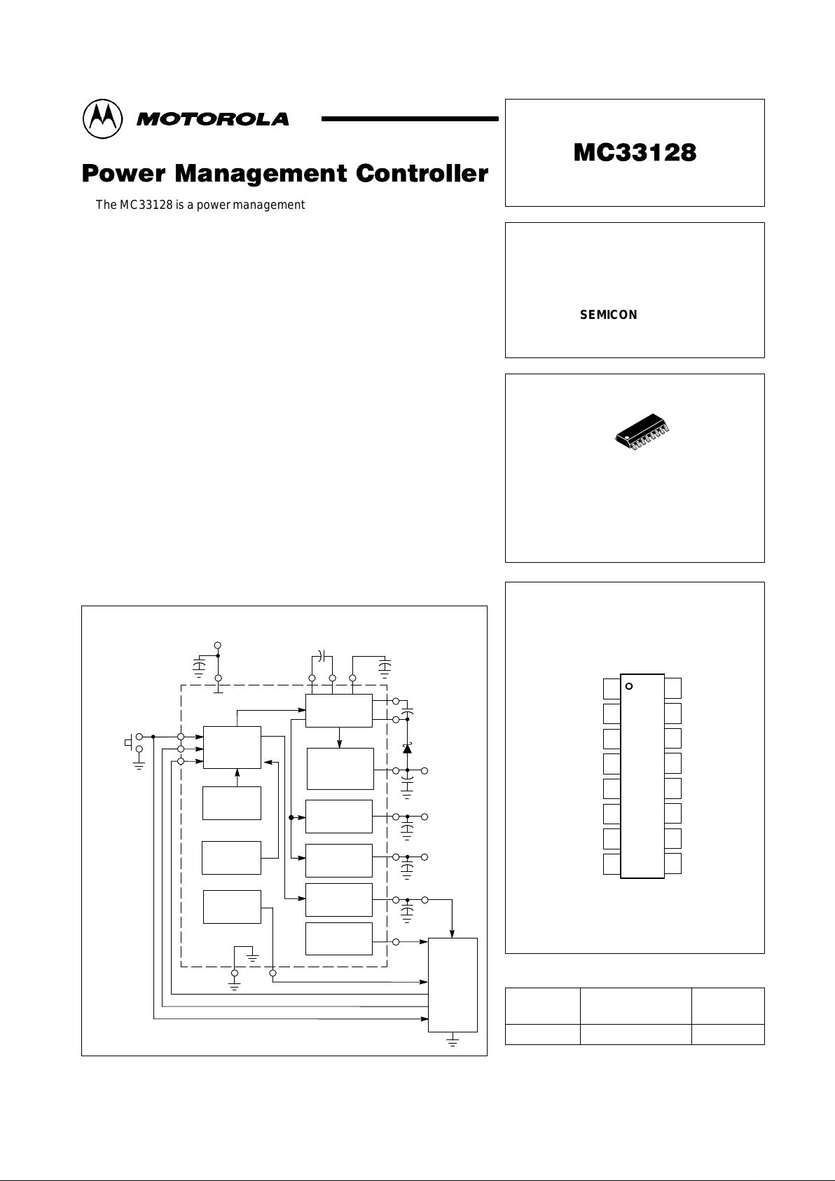
PIN CONNECTIONS
(Top View)
ORDERING INFORMATION
MC33128D TA = – 30° to +60°C SO–16
16
1
Output 2
VBB Charge Pump
Capacitor Input
VBB Charge Pump
Capacitor Drive
Gnd
Output 4 Charge Pump
Capacitor Input
V
CC
Battery Saver Input
VBB Output
Output 4
Output 4 Charge Pump
Capacitor Drive
Output 1
Output 3
Reset Output
Reference Output
Power Up Input
Power Down Input
116
15
14
13
12
11
10
9
2
3
4
5
6
7
8
1
MOTOROLA ANALOG IC DEVICE DATA
The MC33128 is a power management controller specifically designed for
use in battery powered cellular telephone and pager applications. This
device contains all of the active functions required to interface the user to the
system electronics via a microprocessor. This integrated circuit consists of a
low dropout voltage regulator with power–up reset for MPU power, two low
dropout voltage regulators for independant powering of analog and digital
circuitry, and a negative charge pump voltage regulator for full depletion of
gallium arsenide MESFETs.
Also included are protective system shutdown features consisting of a
battery latch that is activated upon battery insertion, low battery voltage
shutdown, and a thermal over temperature detector. This device is available
in a 16–pin narrow body surface mount plastic package.
• Three Positive Regulated Outputs Featuring Low Dropout Voltage
• Negative Regulated Output for Full Depletion of GaAs MESFETs
• MPU Power Up Reset
• Battery Latch
• Low Battery Shutdown
• Pinned–Out Reference for MPU A/D Converter
• Low Start–Up and Operating Current
• Thermal Protection
Simplified Block Diagram
ON/OFF
Toggle
V
CC
VBB CPC
VBB Output
Control
Logic
Low Battery
Shutdown
Thermal
Protection
Reference
Charge
Pump
Negative
Standby
Regulator
Standby
Regulator 1
Standby
Regulator 2
MPU
Regulator
MPU Power
Up Reset
Reference OutputGnd 6 12
9
10
11
16 3 2 4
8
7
5
15
1
14
13
V
DD
V
SS
R
I
O
O
I
Output 4
CPC
Output 4
–2.5 V/1.0 mA
Output 1
3.0 V/30 mA
Output 2
3.0 V/60 mA
Output 3
3.0 V/20 mA
MPU
+
Motorola, Inc. 1996 Rev 0
Page 2
MC33128
2
MOTOROLA ANALOG IC DEVICE DATA
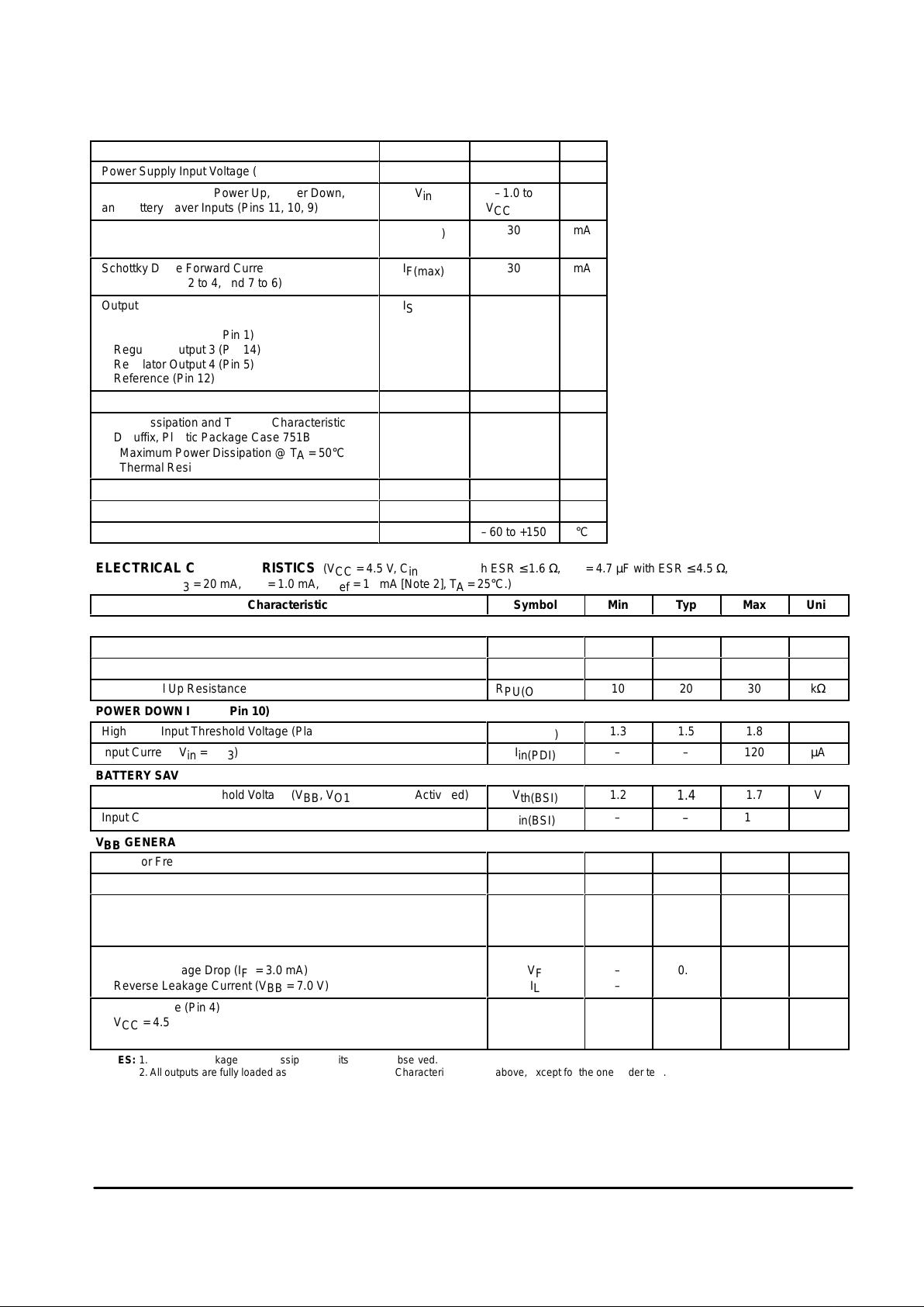
MAXIMUM RATINGS
Rating Symbol Value Unit
Power Supply Input Voltage (Pin 16)
V
CC
+7.0
V
ББББББББББББ
Á
Input Voltage Range Power Up, Power Down,
and Battery Saver Inputs (Pins 11, 10, 9)
ÁÁÁ
Á
V
in
ÁÁÁ
Á
–1.0 to
VCC + 1.0
Á
Á
V
Charge Pump Capacitor Drive Outputs,
Source or Sink Current (Pins 3, 8)
I
O(max)
30
mA
ББББББББББББ
Á
Schottky Diode Forward Current
(Pins 16 to 2, 2 to 4, and 7 to 6)
ÁÁÁ
Á
I
F(max)
ÁÁÁ
Á
30
Á
Á
mA
ББББББББББББ
Á
ББББББББББББ
Á
ББББББББББББ
Á
Output Source Current (Note 1)
Regulator Output 1 (Pin 15)
Regulator Output 2 (Pin 1)
Regulator Output 3 (Pin 14)
Regulator Output 4 (Pin 5)
Reference (Pin 12)
ÁÁÁ
Á
ÁÁÁ
Á
ÁÁÁ
Á
I
Source
ÁÁÁ
Á
ÁÁÁ
Á
ÁÁÁ
Á
150
250
50
10
40
Á
Á
Á
Á
Á
Á
mA
Reset Sink Current (Pin 13)
I
Sink
5.0
mA
ББББББББББББ
Á
ББББББББББББ
Á
Power Dissipation and Thermal Characteristic
D Suffix, Plastic Package Case 751B
Maximum Power Dissipation @ TA = 50°C
Thermal Resistance, Junction–to–Air
ÁÁÁ
Á
ÁÁÁ
Á
P
D
R
∅JA
ÁÁÁ
Á
ÁÁÁ
Á
560
180
Á
Á
Á
Á
mW
°C/W
Operating Junction Temperature
T
J
+150
°C
Operating Ambient Temperature (Note 1)
T
A
–30 to +60
°C
Storage Temperature
T
stg
–60 to +150
°C
ELECTRICAL CHARACTERISTICS (V
CC
= 4.5 V, Cin = 33 µF with ESR ≤ 1.6 Ω, CO = 4.7 µF with ESR ≤ 4.5 Ω, IO1 = 30 mA,
I
O2
= 60 mA, IO3 = 20 mA, IO4 = 1.0 mA, I
Oref
= 10 mA [Note 2], TA = 25°C.)
Characteristic
Symbol Min Typ Max Unit
POWER UP INPUT (Pin 11)
Low State Input Threshold Voltage
V
th(toggle)
VCC – 1.5
VCC – 1.2
VCC – 0.8
V
Input Current (Vin = VO3)
БББББ
I
in(toggle)
–
–
120
ÁÁÁ
µA
Internal Pull Up Resistance
БББББ
R
PU(ON/OFF)
10
20
30
ÁÁÁ
kΩ
POWER DOWN INPUT (Pin 10)
High State Input Threshold Voltage (Places IC in Standby Mode)
БББББ
V
th(PDI)
1.3
1.5
1.8
ÁÁÁ
V
Input Current (Vin = VO3)
БББББ
I
in(PDI)
–
–
120
ÁÁÁ
µA
BATTERY SAVER INPUT (Pin 9)
High State Input Threshold Voltage (VBB, VO1, VO2, VO4 Activated)
БББББ
V
th(BSI)
1.2
1.4
1.7
ÁÁÁ
V
Input Current (Vin = VO3)
БББББ
I
in(BSI)
–
–
120
ÁÁÁ
µA
VBB GENERATOR
Oscillator Frequency
БББББ
f
OSC
85
95
105
ÁÁÁ
kHz
Oscillator Duty Cycle
БББББ
DC
35
50
65
ÁÁÁ
%
БББББББББББББББББ
Á
Charge Pump Capacitor Drive Output Voltage Swing (Pin 3)
High State (I
Source
= 3.0 mA)
Low State (I
Sink
= 3.0 mA)
БББББ
ÁÁÁÁ
Á
V
OH
V
OL
ÁÁ
Á
–
–
ÁÁ
Á
VCC – 0.9
0.15
ÁÁ
Á
–
–
ÁÁÁ
ÁÁ
Á
V
БББББББББББББББББ
Á
Schottky Diode (Pins 2, 4)
Forward Voltage Drop (IF = 3.0 mA)
Reverse Leakage Current (VBB = 7.0 V)
БББББ
ÁÁÁÁ
Á
V
F
I
L
ÁÁ
Á
–
–
ÁÁ
Á
0.5
0.01
ÁÁ
Á
–
–
ÁÁÁ
ÁÁ
Á
V
µA
БББББББББББББББББ
Á
Output Voltage (Pin 4)
VCC = 4.5 V
VCC = 2.9 V
БББББ
ÁÁÁÁ
Á
V
O(VBB)
ÁÁ
Á
–
–
ÁÁ
Á
7.9
4.4
ÁÁ
Á
–
–
ÁÁÁ
ÁÁ
Á
V
NOTES: 1. Maximum package power dissipation limits must be observed.
2.All outputs are fully loaded as stated in the Electrical Characteristics Table above, except for the one under test.
Page 3
MC33128
3
MOTOROLA ANALOG IC DEVICE DATA
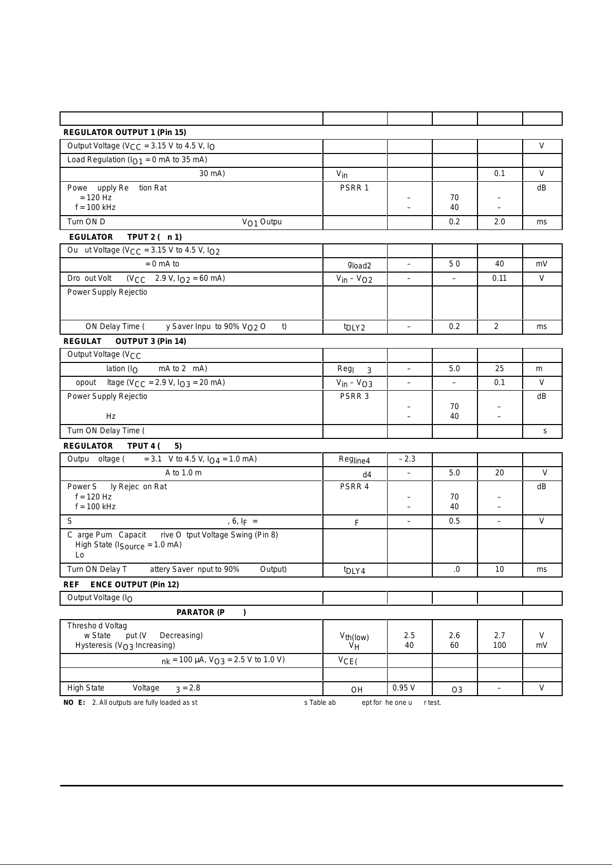
ELECTRICAL CHARACTERISTICS (V
CC
= 4.5 V, Cin = 33 µF with ESR ≤ 1.6 Ω, CO = 4.7 µF with ESR ≤ 4.5 Ω, IO1 = 30 mA,
I
O2
= 60 mA, IO3 = 20 mA, IO4 = 1.0 mA, I
Oref
= 10 mA [Note 2], TA = 25°C.)
Characteristic UnitMaxTypMinSymbol
REGULATOR OUTPUT 1 (Pin 15)
Output Voltage (VCC = 3.15 V to 4.5 V, IO1 = 30 mA)
БББББ
Reg
line1
2.9
3.0
3.1
ÁÁÁ
V
Load Regulation (IO1 = 0 mA to 35 mA)
БББББ
Reg
load1
–
5.0
30
ÁÁÁ
mV
Dropout Voltage (VCC = 2.9 V , IO1 = 30 mA)
БББББ
Vin – V
O1
–
–
0.1
ÁÁÁ
V
БББББББББББББББББ
Á
Power Supply Rejection Ratio
f = 120 Hz
f = 100 kHz
БББББ
ÁÁÁÁ
Á
PSRR 1
ÁÁ
Á
–
–
ÁÁ
Á
70
40
ÁÁ
Á
–
–
ÁÁÁ
ÁÁ
Á
dB
Turn ON Delay Time (Battery Saver Input to 90% VO1 Output)
БББББ
t
DLY1
–
0.2
2.0
ÁÁÁ
ms
REGULATOR OUTPUT 2 (Pin 1)
Output Voltage (VCC = 3.15 V to 4.5 V, IO2 = 60 mA)
БББББ
Reg
2.9
3.0
3.1
ÁÁÁ
V
Load Regulation (IO2 = 0 mA to 60 mA)
БББББ
Reg
load2
–
5.0
40
ÁÁÁ
mV
Dropout Voltage (VCC = 2.9 V , IO2 = 60 mA)
БББББ
Vin – V
O2
–
–
0.11
ÁÁÁ
V
БББББББББББББББББ
Á
Power Supply Rejection Ratio
f = 120 Hz
f = 100 kHz
БББББ
ÁÁÁÁ
Á
PSRR 2
ÁÁ
Á
–
–
ÁÁ
Á
70
40
ÁÁ
Á
–
–
ÁÁÁ
ÁÁ
Á
dB
Turn ON Delay Time (Battery Saver Input to 90% VO2 Output)
БББББ
t
DLY2
–
0.2
2.0
ÁÁÁ
ms
REGULATOR OUTPUT 3 (Pin 14)
Output Voltage (VCC = 3.15 V to 4.5 V, IO3 = 20 mA)
БББББ
Reg
line3
2.9
3.0
3.1
ÁÁÁ
V
Load Regulation (IO3 = 0 mA to 20 mA)
БББББ
Reg
load3
–
5.0
25
ÁÁÁ
mV
Dropout Voltage (VCC = 2.9 V , IO3 = 20 mA)
БББББ
Vin – V
O3
–
–
0.1
ÁÁÁ
V
БББББББББББББББББ
Á
БББББББББББББББББ
Á
Power Supply Rejection Ratio
f = 120 Hz
f = 100 kHz
БББББ
ÁÁÁÁ
Á
ÁÁÁÁ
Á
PSRR 3
ÁÁ
Á
ÁÁ
Á
–
–
ÁÁ
Á
ÁÁ
Á
70
40
ÁÁ
Á
ÁÁ
Á
–
–
ÁÁÁ
ÁÁ
Á
ÁÁ
Á
dB
Turn ON Delay Time (ON/OFF Toggle Input to 90% VO3 Output)
БББББ
t
DLY3
–
0.5
3.0
ÁÁÁ
ms
REGULATOR OUTPUT 4 (Pin 5)
Output Voltage (VCC = 3.15 V to 4.5 V, IO4 = 1.0 mA)
БББББ
Reg
line4
–2.35
–2.5
–2.65
ÁÁÁ
V
Load Regulation (IO4 = 0 mA to 1.0 mA)
БББББ
Reg
load4
–
5.0
20
ÁÁÁ
mV
БББББББББББББББББ
Á
БББББББББББББББББ
Á
Power Supply Rejection Ratio
f = 120 Hz
f = 100 kHz
БББББ
ÁÁÁÁ
Á
ÁÁÁÁ
Á
PSRR 4
ÁÁ
Á
ÁÁ
Á
–
–
ÁÁ
Á
ÁÁ
Á
70
40
ÁÁ
Á
ÁÁ
Á
–
–
ÁÁÁ
ÁÁ
Á
ÁÁ
Á
dB
Schottky Diode Forward Voltage Drop (Pins 7, 6, IF = 1.0 mA)
БББББ
V
F
–
0.5
–
ÁÁÁ
V
БББББББББББББББББ
Á
Charge Pump Capacitor Drive Output Voltage Swing (Pin 8)
High State (I
Source
= 1.0 mA)
Low State (I
Sink
= 1.0 mA)
БББББ
ÁÁÁÁ
Á
V
OH
V
OL
ÁÁ
Á
–
–
ÁÁ
Á
VBB – 0.2 5
0.15
ÁÁ
Á
–
–
ÁÁÁ
ÁÁ
Á
V
Turn ON Delay Time (Battery Saver Input to 90% VO4 Output)
БББББ
t
DLY4
–
4.0
10
ÁÁÁ
ms
REFERENCE OUTPUT (Pin 12)
Output Voltage (IO = 0 mA to 10 mA)
БББББ
Reg
load
1.46
1.5
1.54
ÁÁÁ
V
ББББББББББББББББББББББББББББББББ
MPU POWER UP RESET COMPARATOR (Pin 13)
БББББББББББББББББ
Á
БББББББББББББББББ
Á
Threshold Voltage
Low State Output (VO3 Decreasing)
Hysteresis (VO3 Increasing)
БББББ
ÁÁÁÁ
Á
ÁÁÁÁ
Á
V
th(low)
V
H
ÁÁ
Á
ÁÁ
Á
2.5
40
ÁÁ
Á
ÁÁ
Á
2.6
60
ÁÁ
Á
ÁÁ
Á
2.7
100
ÁÁÁ
ÁÁ
Á
ÁÁ
Á
V
mV
Output Sink Saturation (I
Sink
= 100 µA, VO3 = 2.5 V to 1.0 V)
БББББ
V
CE(sat)
–
130
300
ÁÁÁ
mV
Internal Pull–up Resistance
БББББ
R
PU
10
26
40
ÁÁÁ
kΩ
БББББББББББББББББ
High State Output Voltage (VO3 = 2.8 V)
БББББ
ÁÁÁÁ
V
OH
ÁÁ
0.95 V
O3
ÁÁ
V
O3
ÁÁ
–
ÁÁÁ
ÁÁ
V
NOTE: 2.All outputs are fully loaded as stated in the Electrical Characteristics Table above, except for the one under test.
Page 4

MC33128
4
MOTOROLA ANALOG IC DEVICE DATA
ELECTRICAL CHARACTERISTICS
(VCC = 4.5 V, Cin = 33 µF with ESR ≤ 1.6 Ω, CO = 4.7 µF with ESR ≤ 4.5 Ω, IO1 = 30 mA,
I
O2
= 60 mA, IO3 = 20 mA, IO4 = 1.0 mA, I
Oref
= 10 mA [Note 2], TA = 25°C.)
Characteristic UnitMaxTypMinSymbol
LOW BATTERY SHUTDOWN COMPARATOR (Pin 16)
Shutdown Threshold Voltage (VCC Decreasing, Pin 10 = Gnd)
БББББ
V
th(LBSC)
2.25
2.4
2.55
ÁÁÁ
V
TOTAL DEVICE (Pin 16)
БББББББББББББББББ
Á
БББББББББББББББББ
Á
БББББББББББББББББ
Á
Power Supply Current (No Load On All Outputs)
Operating
Battery Saver Input High (Pin 9 = 2.0 V)
Battery Saver Input Low (Pin 9 ≤ 0.8 V)
Standby (After Power Down Input Strobe)
БББББ
ÁÁÁÁ
Á
ÁÁÁÁ
Á
ÁÁÁÁ
Á
I
CC
ÁÁ
Á
ÁÁ
Á
ÁÁ
Á
–
–
–
ÁÁ
Á
ÁÁ
Á
ÁÁ
Á
2.6
270
8.0
ÁÁ
Á
ÁÁ
Á
ÁÁ
Á
4.0
330
12
ÁÁÁ
ÁÁ
Á
ÁÁ
Á
ÁÁ
Á
mA
µA
µA
NOTE: 2.All outputs are fully loaded as stated in the Electrical Characteristics Table above, except for the one under test.
0
8.0
0
–3.0
0
0
0
160
V ,
O
V OUTPUT VOLTAGE (V)
IO, VBB OUTPUT SOURCE CURRENT (mA)
V
O
, OUTPUT 4 VOL TAGE (V)
IO, OUTPUT 4 SOURCE CURRENT (mA)
V
ref
, OUTPUT VOLTAGE CHANGE (mV)
I
ref
, REFERENCE SOURCE CURRENT (mA)
Figure 1. Dropout Voltage
versus Source Current
Figure 2. Output 4 Voltage
versus Source Current
Figure 3. Reference Output
Voltage Change versus Source Current
IO, OUTPUT SOURCE CURRENT (mA)
Figure 4. VBB Output
Voltage Change versus Source Current
VCC = 2.9 V
TA = 25
°
C
See Note
Output 2
Output 1
Output 3
20 40 60 80 100
120
80
40
0
V – V , DROPOUT VOLTAGE (mV)
Oin
TA = 25°C
See Note
VCC = 3.15 V
–1.0 –2.0 –3.0 –4.0 –5.0
–2.5
–2.0
–1.5
–1.0
–0.5
0
VCC = 4.5 V
TA = 25°C
See Note
VCC = 3.15 V
5.0 10 15 20 25
–10
–20
–30
–40
∆
BB
6.0
4.0
2.0
0
0.5 1.0 1.5 2.0
TA = 25°C
See Note
VCC = 4.5 V
NOTE: All outputs are fully loaded as stated in the Electrical Characteristics Table above, except for the one under test.
Page 5

MC33128
5
MOTOROLA ANALOG IC DEVICE DATA
OPERA TING DESCRIPTION
The MC33128 is a complete power management
controller that is designed to interface the user to the system
electronics via a microprocessor.
Outputs
Three low dropout voltage regulators are provided at outputs
1, 2 and 3. Outputs 1 and 2 were contemplated for independent
powering of the systems analog and digital circuitry. This
significantly reduces the possibility of digitally generated noise
and spurious signals from coupling into the RF and analog
circuits. The low dropout characteristic of Outputs 1 and 2 is
achieved by applying a boosted battery voltage, VBB, to their
respective driver transistors. This allows the output pass
transistors to be driven into saturation when the battery voltage
approaches 3.0 V . The VBB Output appears at Pin 4 and can be
used to provide gate bias for enhancing external N channel
MOSFET switches. Excess ive loading of the V
BB
output will
result in an increase in dropout voltage.
Output 4 is derived from a voltage inverting charge pump
circuit and is intended to provide the negative gate bias
required for full depletion of RF gallium arsenide MESFETs.
In personal communication system applications such as
cellular telephone, negative gate bias is usually required by
the antenna switch and power amplifier circuit blocks with a
typical combined current of less than 1.0 mA. Output 4 can
supply in excess of 2.0 mA, but there will be an increase in
dropout voltage of Outputs 1, 2 and 3.
Outputs 1, 2, 4, VBB Generator and Thermal Protection are
all enabled and disabled in unison by the Battery Saver Input,
Pin 9. The microprocessor can be programmed to
significantly extend the system battery operating time by
periodically enabling the receiver circuitry.
Output 3 provides power to the microprocessor, flash
EPROM and the system display. These blocks are enabled
by the Power Up Input, Pin 11, and disabled by the Power
Down Input, Pin 10. By having separate power up and power
down inputs, the microprocessor can store any pending
information before turning the system and then itself OFF.
This allows a controlled or graceful shutdown. Note that the
power down request is initiated by pressing the toggle switch
while the system is “ON”. This action generates a
microprocessor non–maskable interrupt that initiates the
graceful shutdown.
Battery Voltage Detection
Reverse biasing and eventual failure of the lowest
capacity cell in the battery pack can occur if the system is
accidentally left on for an extended time period. To prevent
this condition the following circuit blocks were incorporated.
A means for low battery detection is accomplished by
using the Reference Output, Pin 12, in conjunction with the
microprocessor’s analog to digital converter input. A
microprocessor output (LBO) can be designated to flash a
display enunciator when a low battery condition exists. The
Reference Output is 1.5 V ±2.7% and is capable of sourcing
in excess of 10 mA.
The Power Up Reset Output, Pin 13, is designed to hold
the microprocessor reset input low until the voltage at Output 3
rises above 2.66 V . This feature prevents the microprocessor
from hanging or writing invalid information into its memory
during power up. Notice that the output of the MPU Power Up
Reset comparator also drives the base of transistor QPD. If
Output 3 should fall below 2.6 V, due to an overload or a low
battery condition, the comparator will drive QPD “ON”,
causing its collector to pull high on the Power Down Input,
immediately forcing the system into standby mode.
Externally pulling down on Pin 13, base of QPD, will also force
the system into standby mode.
A redundant Low Battery Shutdown circuit is included.
This circuit directly monitors the battery voltage and also
forces the system into standby mode when the battery
voltage falls below 2.4 V. To test the functionality of this
circuit, the high state signal generated by transistor QPD must
be clamped low, to prevent resetting the ON/OFF Latch. An
external short or a pull–down, capable of sinking 2.0 mA at
less than 0.8 V, must be connected to Pin 10.
A Battery Latch circuit is designed into the IC to prevent
the system from turning on when the batteries are inserted
into the finished product. This feature is useful for the end
customer as well as the equipment manufacturer. Upon initial
application of battery voltage, the lower comparator (0.7 V
threshold) forces the Battery Latch into a reset state with its
“Q” output low. This in turn triggers a reset of the ON/OFF
Latch via the OR gate and also locks out the set signal
present at the upper input of the AND gate. As the voltage at
Pin 11 rises above (VCC – 1.5 V), the set signal disappears,
leaving the state of the ON/OFF Latch unchanged (reset).
When the voltage at Pin 11 rises above (VCC –1.0 V), the
upper comparator forces the Battery Latch into a set state
causing its “Q” output to go high. This allows the AND gate
and the ON/OFF Latch to receive a set signal from Pin 11.
The initial Battery Latch lockout time is controlled by the
internal 20 kΩ resistor and the external 0.1 µF capacitor.
Page 6

MC33128
6
MOTOROLA ANALOG IC DEVICE DATA
Figure 5. MC33128 Block Diagram
Reference
Oscillator
S
R
S
R
Thermal
Logic
Bias
20k
V
O3
VBB Generator
VBB Charge
Pump Capacitor
3216
0.22
V
CC
33
V
bat
5.0V to 3.0V
1.27V
VCC –1.0V
Battery
Latch
1.0
µ
A
10pF
0.7V
VCC –1.5V
Power Up
Input
Battery
Saver
Input
Power
Down
Input
Reference
1.5V/10mA
V
O3
1.27V
Reference
Output
Low Battery
Shutdown
V
O3
1.27V
MPU
Power Up
Reset
1.27V
MPU
Regulator
V
O3
1.27V
26k
40k
V
CC
Q
PD
Reset
Output
4.7
Output 3
3.0V/20mA
Output 2
3.0V/60mA
Output 1
3.0V/30mA
Output 4
–2.5V/1.0mA
Output 4
Charge Pump Capacitor
1.27V
1.27V
Standby
Regulator 2
Standby
Regulator 1
–2.5V
Regulator
V
BB
V
BB
1.27V
V
BB
ON/OFF
Latch
11
9
10
12 Gnd 6
ON/OFF
T oggle
Low Battery
Output
V
bat
V
DD
V
SS
LBO
A/D
In
R
Ref
Out
Out
Out
In
13
14
1
15
5
7
8
4
4.7
4.7
4.7
4.7
0.1
Q
Q
MPU
Page 7

MC33128
7
MOTOROLA ANALOG IC DEVICE DATA
Oscillator
VBB Generator
3216
0.22
33
V
bat
V
BB
5
7
8
4
4.7
Figure 6. Voltage Tripler and Switch Driver
4.7
0.1
V
bat
Tripler
Output
ON/OFF
Controlled
Turn ON/OFF
Time
R
C
1
C
2
R
FB
R
L
Load Current
(mA)
VCC = 3.15 V VCC = 4.5 V
Tripler Output Voltage
0
0.5
1.0
1.5
2.0
7.96
7.48
7.24
6.99
6.62
12.01
11.54
11.29
11.04
10.69
Load Turn ON/OFF Time
High R
FB
Critical R
FB
Low R
FB
External Switch
A low threshold N–channel MOSFET can be used to
switch the transmitting power amplifier (RL) ON and OFF. T o
ensure that all of the available battery voltage appears
across the load, the MOSFET must be fully enhanced over
the system’s required operating voltage range. With the
addition of two Schottky diodes and two capacitors, the V
BB
Generator can be made to function as a voltage tripler. The
table in Figure 6 shows the output voltage characteristics of
the tripler circuit.
In order to minimize adjacent channel splatter, the RF
power amplifier must be turned ON and OFF in a controlled
(soft) manner. The applied voltage rise and fall time, as well
as the rate of change in rise and fall time, must be tailored to
the amplifiers characteristics. The circuit consisting of
resistors R, RFB, and capacitors C1 and C2 is a simple
solution allowing the system designer a means to control the
ON and OFF time as well as the waveshape. Feedback
resistor RFB controls the waveshape. Capacitors C
1
and C
2
are usually of equal value.
Page 8

MC33128
8
MOTOROLA ANALOG IC DEVICE DATA
OUTLINE DIMENSIONS
D SUFFIX
PLASTIC PACKAGE
CASE 751B–05
(SO–16)
ISSUE J
0.25 (0.010) T B A
M
S S
MIN MINMAX MAX
MILLIMETERS INCHES
DIM
A
B
C
D
F
G
J
K
M
P
R
9.80
3.80
1.35
0.35
0.40
0.19
0.10
0
°
5.80
0.25
10.00
4.00
1.75
0.49
1.25
0.25
0.25
7
°
6.20
0.50
0.386
0.150
0.054
0.014
0.016
0.008
0.004
0
°
0.229
0.010
0.393
0.157
0.068
0.019
0.049
0.009
0.009
7
°
0.244
0.019
1.27 BSC 0.050 BSC
NOTES:
1. DIMENSIONING AND TOLERANCING PER ANSI
Y14.5M, 1982.
2. CONTROLLING DIMENSION: MILLIMETER.
3. DIMENSION A AND B DO NOT INCLUDE MOLD
PROTRUSION.
4. MAXIMUM MOLD PROTRUSION 0.15 (0.006)
PER SIDE.
5. DIMENSION D DOES NOT INCLUDE DAMBAR
PROTRUSION. ALLOWABLE DAMBAR
PROTRUSION SHALL BE 0.127 (0.005) TOTAL
IN EXCESS OF THE D DIMENSION AT
MAXIMUM MATERIAL CONDITION.
1
8
916
–A
–
–B
–
D 16 PL
K
C
G
–T
–
SEATING
PLANE
R X 45°
M
J
F
P
8 PL
0.25 (0.010) B
M M
Motorola reserves the right to make changes without further notice to any products herein. Motorola makes no warranty, representation or guarantee regarding
the suitability of its products for any particular purpose, nor does Motorola assume any liability arising out of the application or use of any product or circuit, and
specifically disclaims any and all liability, including without limitation consequential or incidental damages. “T ypical” parameters which may be provided in Motorola
data sheets and/or specifications can and do vary in different applications and actual performance may vary over time. All operating parameters, including “Typicals”
must be validated for each customer application by customer’s technical experts. Motorola does not convey any license under its patent rights nor the rights of
others. Motorola products are not designed, intended, or authorized for use as components in systems intended for surgical implant into the body, or other
applications intended to support or sustain life, or for any other application in which the failure of the Motorola product could create a situation where personal injury
or death may occur. Should Buyer purchase or use Motorola products for any such unintended or unauthorized application, Buyer shall indemnify and hold Motorola
and its officers, employees, subsidiaries, affiliates, and distributors harmless against all claims, costs, damages, and expenses, and reasonable attorney fees
arising out of, directly or indirectly, any claim of personal injury or death associated with such unintended or unauthorized use, even if such claim alleges that
Motorola was negligent regarding the design or manufacture of the part. Motorola and are registered trademarks of Motorola, Inc. Motorola, Inc. is an Equal
Opportunity/Affirmative Action Employer.
How to reach us:
USA/EUROPE/Locations Not Listed: Motorola Literature Distribution; JAP AN: Nippon Motorola Ltd.; Tatsumi–SPD–JLDC, 6F Seibu–Butsuryu–Center,
P.O. Box 20912; Phoenix, Arizona 85036. 1–800–441–2447 or 602–303–5454 3–14–2 Tatsumi Koto–Ku, Tokyo 135, Japan. 03–81–3521–8315
MFAX: RMF AX0@email.sps.mot.com – TOUCHT ONE 602–244–6609 ASIA/ PACIFIC: Motorola Semiconductors H.K. Ltd.; 8B Tai Ping Industrial Park,
INTERNET: http://Design–NET .com 51 Ting Ko k Road, Tai Po, N.T., Hong Kong. 852–26629298
MC33128/D
*MC33128/D*
◊
 Loading...