

Page 1
MOTOROLA
SEMICONDUCTOR
TECHNICAL DATA
Advance Information
Low Voltage Compander
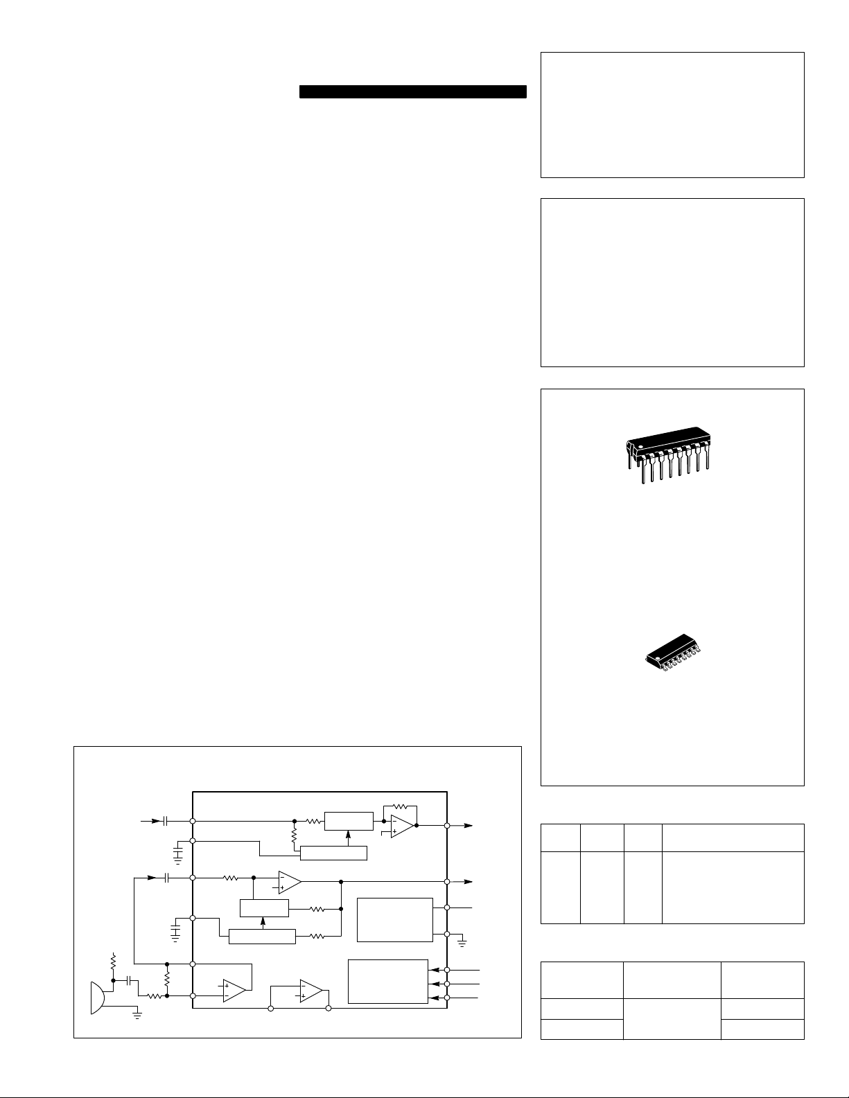
The MC33111 contains two variable gain circuits configured for
compressing and expanding the dynamic range of an audio signal. One
circuit is configured as an expander, and the other is configured as a
compressor. Each circuit has a full wave rectifier to provide average value
information to a variable gain cell located in either the input stage or the
feedback path. An internal temperature stable bandgap reference provides
the necessary precision voltages.
Included in the MC33111 are controls for muting each section
independently, and for passthrough of both. Two uncommitted op amps
are available for peripheral functions.
The MC33111 will operate from a supply voltage of 3.0 V to 7.0 V, and
over a temperature range of – 40° to + 85°C. It is designed to
accommodate a 60 dB dynamic range; from – 40 dB to + 20 dB referenced
to 100 mVrms.
Order this data sheet by MC33111/D
MC33111
LOW VOLTAGE
COMPANDER
SILICON MONOLITHIC
INTEGRATED CIRCUIT
Applications include cordless telephone, CBs, walkie-talkies, and most
voice RF links, and any application where an improvement in the signal to
noise ratio is desired. Other applications include speakerphones and voice
activated intercoms, dictating machines, etc.
• Operating Supply Voltage: 3.0 V to 7.0 V
• Output Voltage Swing = 2.8 V
with VCC = 3.0 V
p-p
• No Precision External Components Required
• 60 dB Dynamic Range Compressed to 30 dB, Re-expandable to 60 dB
• Unity Gain Level set at 100 mVrms
• Attack and Decay Times Adjustable
• Mute and Passthrough Controls
• Two Uncommitted Op Amps
• Temperature Compensated Reference
• Available in Standard DIP and Surface Mount Packages
Simplified Block Diagram
MC33111
0.5
1.0
1.0
µ
0.5
µ
14
11
F
10 k
3
Vb
∆
5
F
10
Vb
9
Gain
Rectifier
Expander
Input
Compressor
Input
V+
Microphone
This document contains information on a new product. Specifications and information herein are subject to change
without notice. This device contains 329 active transistors.
40 k
Vb
15 k
Rectifier
7.5 k
40 k
∆
67
Gain
20 k
Vb
Bias &
Reference
Generator
Mute/
Passthrough
Logic
Expander
Output
15
Compressor
Output
2
16
V
CC
1
4
12
8
CM
EM
PT
16
1
P SUFFIX
PLASTIC PACKAGE
CASE 648
16
1
D SUFFIX
PLASTIC PACKAGE
CASE 751B
(SO-16)
TRUTH TABLE
CM PT Function
EM
0
0
1
X
X
1
0
0
0
X
X
1
Normal
Comp. Mute
Expander Mute
Passthrough
ORDERING INFORMATION
Temperature
Device
MC33111D
MC33111P
Range
–40° to + 85°C
Package
Plastic DIP
Motorola, Inc. 1994
SO-16
Page 2
PIN FUNCTION DESCRIPTION
Name Pin Description
Ground 1
Compressor Output 2
Compressor Input 3
Compressor Mute 4
Compressor Filter 5
Amplifier #1 6, 7
Passthrough 8
Amplifier #2 9, 10
Expander Filter 11
Expander Mute 12
No Connect 13
Expander Input 14
Expander Output 15
V
CC
16
Connect to a clean power supply ground.
Output of the compressor section.
Compressor input. The input impedance is nominally 10 kΩ. Nominal signal range is
1.0 mVrms to 1.0 V rms in normal mode, and up to 0.8 Vrms in passthrough mode.
Must be capacitor coupled to the signal source.
A logic high mutes the compressor. A logic low permits normal operation and passthrough.
Connect an external capacitor to filter the full wave rectifier’s output.
This capacitor affects attack and decay times, and low frequency accuracy.
Inverting input (7) and output (6) of an op amp internally referenced to Vb.
A logic high sets the gain of both expander and compressor to ≈ 0 dB, independent of
input level.
Inverting input (9) and output (10) of an op amp internally referenced to Vb.
Connect an external capacitor to filter the full wave rectifier’s output.
This capacitor affects attack and decay times, and low frequency accuracy.
A logic high mutes the expander. A logic low permits normal operation and passthrough.
This pin is not internally connected to anything.
Expander input. The input impedance is nominally 10.9 kΩ. Nominal signal range is
10 mVrms to 316 mV rms in normal mode, and up to 1.0 Vrms in passthrough mode.
Must be capacitor coupled to the signal source.
Output of the expander section.
Power supply . Connect to a power supply voltage in the range of 3.0 V to 7.0 V.
Bypass capacitor should be provided at this pin.
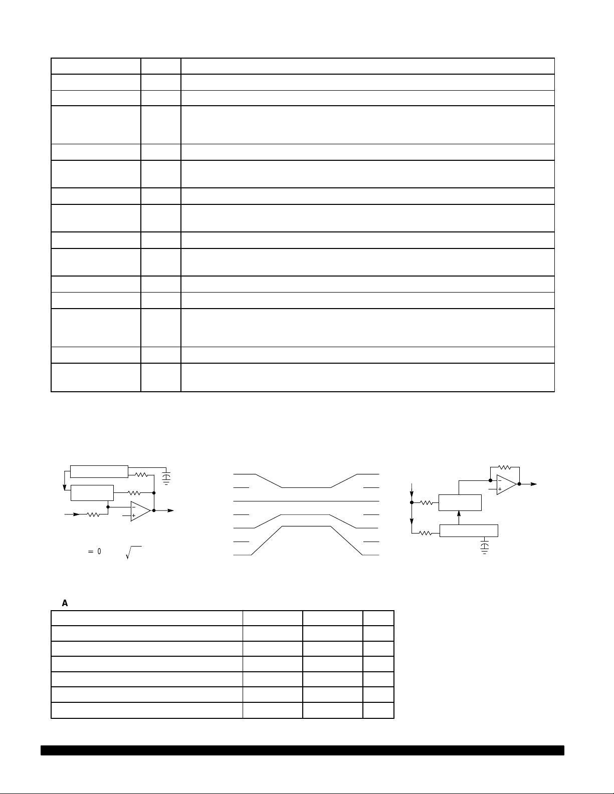
TRANSFER FUNCTIONS
Compressor
Rectifier
∆
Gain
V
V
in
V
out
10 k
+
0.3162 x V
Vb
Ǹ
in
out
MAXIMUM RATINGS
Rating Symbol Value Unit
VCC Supply Voltage (Pin 16 – Pin 1) V
High Input Voltage (Pins 3, 4, 8, 12, 14) V
Low Input Voltage (Pins 3, 4, 8, 12, 14) V
Output Source Current (Pins 2, 6, 10, 15) IO+ Self-limiting mA
Output Sink Current (Pins 2, 6, 10, 15) IO– Self-limiting mA
Storage Temperature T
NOTE: Devices should not be operated at these limits. The “Recommended Operating Conditions”
provides for actual device operation.
Compression Expansion
1.0 V
20 dB
10 dB
0 dB
–10 dB
– 20 dB
– 30 dB
– 40 dB
100 mV
10 mV
1.0 mV
316 mV
31.6 mV
10 mV
(Voltages are rms)
CC
IH
IL
stg
–0.5, +12 Vdc
VCC + 0.5 Vdc
– 0.5 Vdc
– 65, +150 °C
Expander
V
in
∆
Gain
Rectifier
V
out
Vb
= 10 x V
2
in
15 k
40 k
V
out
MOTOROLA MC33111
2
Page 3
RECOMMENDED OPERATING CONDITIONS
Characteristic Symbol Min Typ Max Unit
VCC Supply Voltage V
Input Signal Voltage Range (3.0 V < VCC < 7.0 V) V
Compressor — Normal and Mute Mode 0 — 1.3 Vrms
— Passthrough Mode 0 — 0.8
Expander — Normal Mode 0 — 0.32
— Mute Mode 0 — 1.3
— Passthrough Mode 0 — 1.0
Frequency Range (± 1.0 dB accuracy) Fin 0.300 — 10 kHz
Logic Input Voltage Range (Pins 4, 8, 12) V
Operating Ambient Temperature T
NOTE: All limits are not necessarily functional concurrently.
ELECTRICAL CHARACTERISTICS (V
Characteristic Symbol Min Typ Max Unit
COMPRESSOR (Pin 4 = Low unless noted)
0 dB Gain (Vin = 100 mVrms) G
Gain tracking relative to G
Vin = 1.0 Vrms 9.0 10 11
Vin = 1.0 mVrms –21 –20 –19
Passthrough Gain (Pin 8 = High, Pin 4 = Low, Vin = 1.0 Vrms) G
Muting (∆ Gain) with Pin 4 = High (Vin = 1.0 Vrms) G
Max. Output Swing @ Pin 2 (3.0 V < VCC < 7.0 V) V
Normal Mode — 1.1 —
Passthrough Mode — 2.3 —
Peak Output Current (3.0 ≤ VCC ≤ 7.0 V, Normal or Passthrough Modes,
Vin = Max)
Total Harmonic Distoration (Vin = 100 mVrms) THD — 0.2 1.0 %
Power Supply Rejection @ 1.0 KHz PSRR dB
Vin (Pin 3) = 0 — 37 —
Vin (Pin 3) = 10 mVrms — 64 —
Vin (Pin 3) = 1.0 Vrms — 72 —
Attack Time (Capacitor @ Pin 5 = 1.0 µF, per EIA-553)
Decay Time (Capacitor @ Pin 5 = 1.0 µF, per EIA-553)
Input Impedance at Pin 3 Rin 8.0 10 14 kΩ
DC Bias Level (Pin 2)
Output DC Shift (Vin Changed from 0 to 100 mVrms)
OC
= 3.6 V, f = 1.0 kHz, TA = + 25°C, unless noted.)
CC
CC
in
in
A
OC
G
TC
PTC
MTC
out
I
PK
t
AT(C)
t
D(C)
Vb
IAS
3.0 — 7.0 Vdc
0 — V
–40 — +85 °C
–1.5 0 1.5 dB
– 2.0 0 1.0 dB
55 67 — dB
— ± 4.0 — mA
—
—
1.4
–20
3.0
14
Vb
1.6
CC
—
—
1.6
2.0
mVdc
Vdc
dB
V
p-p
ms
Vdc
EXPANDER (Pin 12 = Low, unless noted)
0 dB Gain (Vin = 100 mVrms) G
Gain Tracking Relative to G
Vin = 316 mVrms 19 20 21
Vin = 10 mVrms –41 –40 –39
Passthrough Gain (Pin 8 = High, Pin 12 = Low, Vin = 1.0 Vrms) G
Muting (∆ Gain) with Pin 12 = High (Vin = 0.316 Vrms) G
Max. Output Swing @ Pin 15 (3.0 V < VCC , 7.0 V) V
Normal Mode — 2.8 —
Passthrough Mode — 2.8 —
Peak Output Current I
VCC = 3.0 V, V
VCC = 3.0 V, V
VCC ≥ 3.6 V, V
Total Harmonic Distoration (Vin = 100 mVrms) THD — 0.2 1.0 %
out
out
out
≤ 2.4 V
= 2.7 V
≤ 2.8 V
OE
p-p
p-p
p-p
G
PTE
MTE
out
PK
OE
TE
–1.5 0 1.5 dB
–1.0 0 2.0 dB
60 76 — dB
— ± 3.5 —
— ±1.0 —
— ± 4.0 —
MOTOROLAMC33111
V
dB
p-p
mA
3
Page 4
ELECTRICAL CHARACTERISTICS (V
Characteristic UnitMaxTypMinSymbol
EXPANDER (Pin 12 = Low, unless noted)
Power Supply Rejection @ 1.0 kHz PSRR dB
Vin (Pin 14) = 0 — 74 —
Vin (Pin 14) = 10 mVrms — 76 —
Vin (Pin 14) = 316 mVrms — 62 —
Attack Time (Capacitor @ Pin 11 = 1.0 µF, per EIA-553)
Decay Time (Capacitor @ Pin 11 = 1.0 µF, per EIA-553)
Input Impedance at Pin 14 R
DC Bias Level (Pin 15)
Output DC Shift (Vin changed from 0 to 100 mVrms)
LOGIC INPUTS (Pins 4, 8, 12)
Switching Threshold (3.0 < VCC < 7.0 V) V
Input Current Rin µA
@ Vin = 0 V — 0 —
@ Vin = 3.6 V — 55 —
Timing (Vin @ Pins 3 and 14 = 300 mVrms, See Figures 1, 2) µs
Comp. Mute (Pin 4) to Comp. Output Low-to-High t
Exp. Mute (Pin 12) to Exp. Output Low-to-High t
Passthrough (Pin 8) to Comp. Output Low-to-High t
Passthrough (Pin 8) to Exp. Output Low-to-High t
OP AMPS (Pins 6, 7, 9, 10)
Open Loop Gain A
Gain Bandwidth BW — 300 — kHz
Input Bias Current @ Pins 7, 9 I
Max Output Swing @ Pins 6, 10 (3.0 V < VCC < 7.0 V) V
Peak Output Current I
VCC = 3.0 V, V
VCC = 3.0 V, V
VCC ≥ 3.6 V, V
Total Harmonic Distoration (V
MISCELLANEOUS
Power Supply Current I
@ VCC = 3.6 V — 1.5 2.0
@ VCC = 7.0 V — 1.7 —
Reference Voltage Vb — 1.5 — Vdc
Channel Separation CS dB
Expander to Compressor
(Pin 14 = 316 mVrms @ 1.0 kHz and Pin 3 = 0 mVrms) 40 70 —
(Pin 14 = 100 mVrms (300 Hz < f < 20 kHz),
Pin 3 = 100 mVrms @ 1.2 kHz) — 96 —
Compressor to Expander
(Pin 3 = 1.0 Vrms @ 1.0 kHz and Pin 14 = 0 mVrms) 60 100 —
(Pin 3 = 100 mVrms (300 Hz < f < 20 kHz),
Pin 14 = 100 mVrms @ 1.2 kHz) — 97 —
out
out
out
≤ 2.4 V
= 2.6 V
≤ 2.8 V
p-p
p-p
p-p
= 1.0 Vrms, Unity Gain) THD — 0.02 0.2 %
out
= 3.6 V, f = 1.0 kHz, TA = + 25°C, unless noted.)
CC
t
AT(E)
t
D(E)
in
Vb
IAS
ST
High-to-Low t
High-to-Low t
High-to-Low t
High-to-Low t
CMLH
CMHL
EMLH
EMHL
PCLH
PCHL
PELH
PEHL
VOL
IB
out
PK
CC
—
—
8.0 10.9 14 kΩ
1.4
–20
— 1.3 — Vdc
— 2.0 —
— 3.0 —
— 2.0 —
— 3.0 —
— 2.0 —
— 5.0 —
— 6.0 —
— 7.0 —
— 100 — dB
— 8.0 — nA
— 2.8 — V
— ± 3.0 —
— ± 2.0 —
— ± 3.7 —
3.0
14
Vb
1.0
—
—
1.6
20
mVdc
ms
Vdc
p-p
mA
mA
MOTOROLA MC33111
4
Page 5
TEMPERATURE PERFORMANCE (Typical performance based on device characterization, not guaranteed.)
Characteristic –40°C +25°C +85°C
Power Supply Current
@ VCC = 3.6 V 1.2 mA 1.5 mA 1.6 mA
@ VCC = 7.0 V 1.4 mA 1.7 mA 1.9 mA
Reference Voltage (Vb) 1.495 V 1.5 V 1.505 V
0 dB Gain (Vin = 100 mVrms) — Compressor 0.08 dB 0 dB – 0.04 dB
0 dB Gain (Vin = 100 mVrms) — Expander 0.04 dB 0 dB – 0.03 dB
Total Harmonic Distortion (Vin = 100 mVrms) — Compressor 0.3% 0.2% 0.2%
Total Harmonic Distortion (Vin = 100 mVrms) — Expander 0.3% 0.2% 0.16%
Gain Tracking Relative to 0 dB Gain — Compressor
Vin = 1.0 Vrms 10.8 dB 10 dB 10 dB
Vin = 1.0 mVrms –19.95 dB – 20 dB – 20.1 dB
Gain Tracking Relative to 0 dB Gain — Expander
Vin = 316 mVrms 18.6 dB 20 dB 19.95 dB
Vin = 10 mVrms – 40.2 dB – 40 dB – 39.9 dB
Muting (∆ Gain) with Pin 4 = High (Vin = 1.0 Vrms) — Compressor 68 dB 67 dB 66 dB
Muting (∆ Gain) with Pin 12 = High (Vin = 0.316 Vrms) — Expander 76 dB 76 dB 75 dB
Figure 1. Mute Timing
Compressor
or Expander
Mute Input
Compressor
or Expander
Output
Passthrough
Input
Compressor
Output
Expander
Output
t
EMLH
t
CMLH
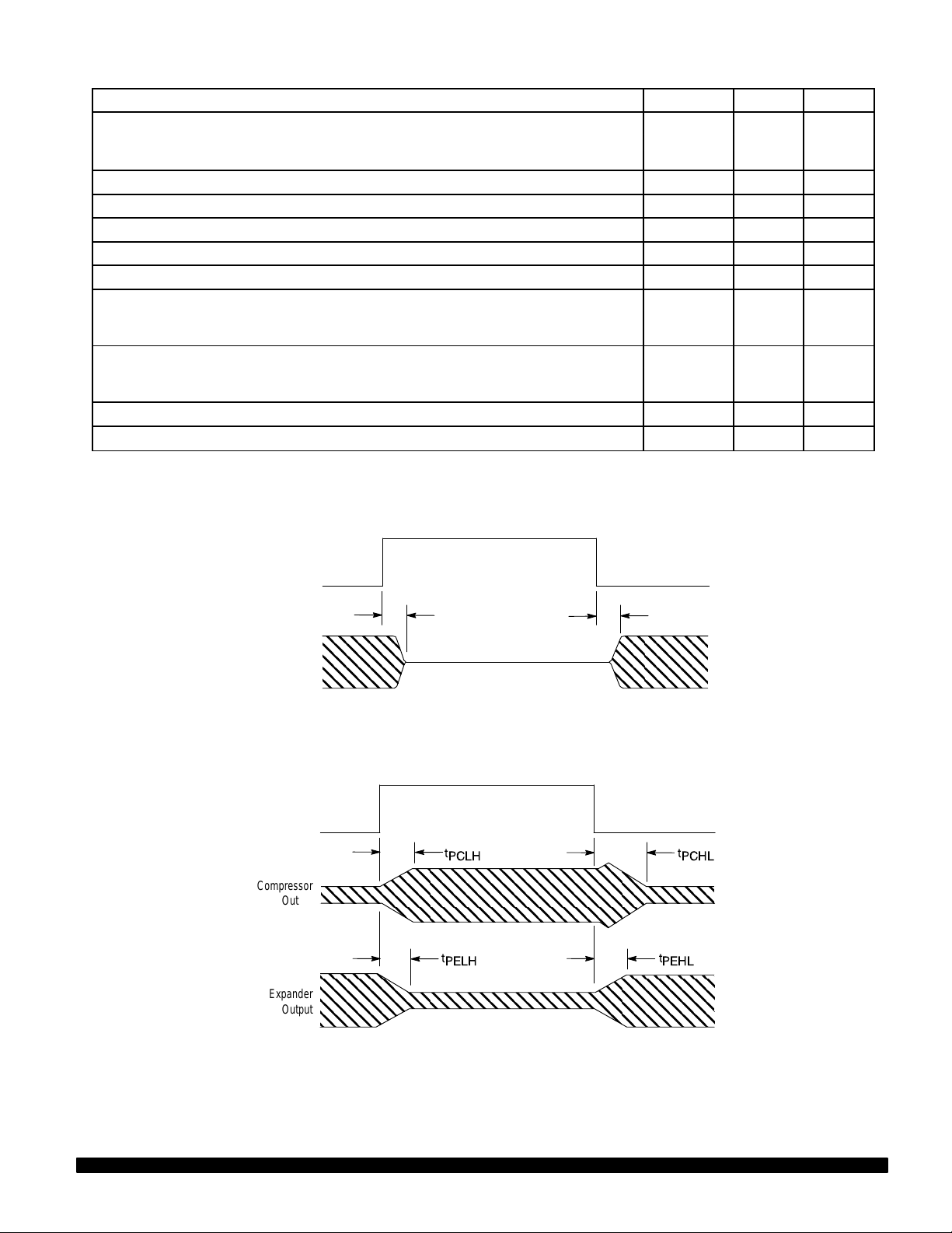
Figure 2. Passthrough Timing
t
PCLH
t
PELH
t
CMHL
t
EMHL
t
PEHL
t
PCHL
MOTOROLAMC33111
5
Page 6

1000
Figure 3. Transfer Characteristics
Figure 4. Transfer Characteristics
20
–20
, OUTPUT VOL TAGE (dB)
out
V
–40
0
Compressor
Expander
–40
Vin, INPUT VOLTAGE (dB)
, OUTPUT VOL TAGE (mVrms)
out
V
100
10
1.0
1.0
Compressor
Expander
100010 100 – 20 0 20
Vin, INPUT VOLTAGE (mVrms)
Figure 5. Frequency Response (Compressor) Figure 6. Frequency Response (Expander)
– 5.0
–15
–25
OUTPUT RELA TIVE T O INPUT (dB)
–35
15
5.0
Vin = 316 mVrms
Vin = 100 mVrms
0
Vin = 31.6 mVrms
Vin = 10 mVrms
100
f, FREQUENCY (Hz)
– 5.0
–10
OUTPUT RELA TIVE T O INPUT (dB)
–15
25
20
15
10
5.0
0
100
Vin = 1.0 mVrms
Vin = 10 mVrms
Vin = 100 mVrms
Vin = 1.0 Vrms
1000 10k 100k 1000 10k 100k
f, FREQUENCY (Hz)
0 dB = 100 mVrms
Figure 7. Attack and Decay Times (Compressor)
V1
Output
(Pin 2)
90 mV
Input
(Pin 3)
Attack Time = Time to 1.5 x V1 from input increase.
Decay Time = Time to 0.75 x V2 from input decrease.
Test per EIA-553.
MOTOROLA MC33111
6
V2
360 mV
Figure 8. Attack and Decay Times (Expander)
Output
(Pin 15)
Input
(Pin 14)
Attack Time = Time to 0.57 x V1 from input increase.
Decay Time = Time to 1.5 x V2 from input decrease.
Test per EIA-553.
V1
100 mV
V2
200 mV
Page 7

Figure 9. Attack and Decay Times (Compressor)
100
Figure 10. Attack and Decay Times (Expander)
100
t, TIME (ms)
°
80
60
40
20
1.0
0
0
1.0 2.0 3.0 4.0 5.0
C, CAPACITANCE AT PIN 5 (µF)
Figure 11. Compressor Gain Tracking
versus T emperature
0
Decay Time
Attack Time
t, TIME (ms)
°
80
60
40
20
2.0
1.0
Decay Time
0
0
1.0 2.0 3.0 4.0 5.0
C, CAPACITANCE AT PIN 11 (
Attack Time
µ
F)
Figure 12. Expander Gain Tracking
versus T emperature
0
GAIN DRIFT VS +25 C (dB)
–1.0
–40
Figure 13. THD versus T emperature Figure 14. Logic Inputs’ Current
1.0
0.5
TOTAL HARMONIC DISTORTION (%)
0
–40
– 20 0 20 40 60 85 2.0 4.0 6.0 7.0
Shaded area depicts typical drift range
1.0 mVrms
≤
Vin ≤ 1.0 Vrms
TA, AMBIENT TEMPERATURE (°C)
Compressor
Expander
–1.0
GAIN DRIFT VS +25 C (dB)
– 2.0
–40
120
100
80
µ
60
40
, INPUT CURRENT ( A)
20
in
I
0
0
Shaded area depicts typical drift range
10 mVrms
≤
Vin ≤ 316 mVrms
04020–20 60 85– 20 0 20 40 60 85
TA, AMBIENT TEMPERATURE (°C)TA, AMBIENT TEMPERATURE (°C)
Vin, INPUT VOLTAGE (V)
Pins 4, 8, 12
Vin
≤
V
CC
MOTOROLAMC33111
7
Page 8

FUNCTIONAL DESCRIPTION
Introduction
The MC33111 compander (COMpressor and exPANDER)
is composed of two variable gain circuits which provide
compression and expansion of a signal’s dynamic range. The
compressor will take a signal with a 60 dB dynamic range (1.0
mV to 1.0 Vrms), and reduce that to a 30 dB dynamic range
(10 mV to 316 mV) by attenuating strong signals, while
amplifying low level signals. The expander does the opposite
in that the 30 dB signal range is increased to a dynamic range
of 60 dB by amplifying strong signals and attenuating low level
signals. The 0 dB level is internally set at 100 mVrms — that is
the signal level which is neither amplified nor attenuated. Both
circuits contain the necessary precision full wave rectifier,
variable gain cell, and temperature compensated references
required for accurate and stable performance.
Figure 15. Compressor
5
µ
F
1.0
Both the compressor and expander can be muted
independently by the use of Pins 4 and 12, respectively. A
minimum of 55 dB of muting is guaranteed for the
compressor, and 60 dB for the expander. A passthrough
function (Pin 8) is provided which sets both sections to unity
gain, regardless of input level.
Two uncommitted op amps are provided which can be
used for perpherial functions. Each is internally biased at Vb
(≈ +1.5 V), and has a bandwidth of ≈ 300 kHz.
NOTE: All dB values mentioned in this data sheet, unless
otherwise noted, are referenced to 100 mVrms.
Rectifier
40 k
I
ref
V
CC
3
Input
10 k
Vb
Compressor
The compressor is a noninverting amplifier with a fixed
input resistor and a variable gain cell in its feedback path as
shown in Figure 15.
The amplifier output is sampled by the precision rectifier
which, in turn, supplies a DC signal (I
CONTROL
), representative of the rectifier’s AC signal, to the variable gain cell. The
reference current (I
) is an internally generated precision
REF
current. The effective impedance of the variable gain cell
varies with the ratio of the two currents, and decreases as
I
CONTROL
increases, thereby providing compression. The
output is related to the input by the following equation
(Vin and V
V
out
out
+
are rms volts):
0.3162 x V
Ǹ
in
(1)
In terms of dB levels, the relationship is:
Vo(dB) = 0.5 x Vi(dB) (2)
where 0 dB = 100 mVrms (See Figures 3 and 4).
The input and output are internally biased at Vb (≈ +1.5 V),
and must therefore be capacitor coupled to external circuitry.
Pin 3 input impedance is nominally 10 kΩ (± 20%), and the
maximum functional input signal is listed in the Recommended
I
CONTROL
∆
Gain
7.5 k
2
Output
Operating Conditions table. Bias currents required by the op
amp and the variable gain cell are internally supplied. Due to
clamp diodes at the input (to VCC and ground), the input signal
must be maintained between the supply rails. If the input signal
goes more than 0.5 V above VCC or below ground, excessive
currents will flow, and distortion will show up at the output and
possibly in other parts of the circuit.
When AC signals are not present at the input, the variable
gain cell will attempt to set a very high gain to comply with
Equation 2. An internal clamp limits the maximum gain to
≈ 26 dB to prevent instabilities.
The output of the rectifier is filtered by the capacitor at
Pin 5, which, in conjunction with an internal 20 k resistor,
provides the time constant for the attack and decay times.
The attack and decay times listed in the Electrical
Characteristics were determined using the test procedure
defined in EIA-553. Figure 9 indicates how the times vary
with the capacitor value. If the attack and decay times are
decreased using a smaller capacitor, performance at low
frequencies will degrade.
MOTOROLA MC33111
8
Page 9

Figure 16. Expander
40 k
V
CC
Input
14
15 k
I
ref
Expander
The expander is an noninverting amplifier with a fixed
feedback resistor and a variable gain cell in its input path as
shown in Figure 16.
The input signal is sampled by the precision rectifier which, in
turn, supplies a DC signal (I
CONTROL
), representative of the AC
input signal, to the variable gain cell. The reference current
(I
) is an internally generated precision current. The effective
REF
impedance of the variable gain cell varies with the ratio of the
two currents, and decreases as I
CONTROL
increases, thereby
providing expansion. The output is related to the input by the
following equation (Vin and V
V
= 10 x (Vin)
out
2
are rms volts):
out
(3)
In terms of dB levels, the relationship is:
Vo(dB) = 2.0 x V i(dB) (4)
where 0 dB = 100 mVrms (See Figures 3 and 4).
The input and output are internally biased at Vb (≈ +1.5 V),
and must therefore be capacitor coupled to external circuitry .
The input impedance at Pin 14 is nominally 10.9 kΩ (± 20%),
and the maximum functional input signal is listed in the
Recommended Operating Conditions table. Bias currents
required by the op amp and the variable gain cell are
internally supplied. Due to clamp diodes at the input (to V
CC
and ground), the input signal must be maintained between
the supply rails. If the input signal goes more than 0.5 V
above VCC or below ground, excessive currents will flow, and
distortion will show up at the output, and possibly in other
parts of the circuit.
The output of the rectifier is filtered by the capacitor at
Pin 11, which, in conjunction with an internal 20 k resistor,
provides the time constant for the attack and decay times.
The attack and decay times listed in the Electrical
Characteristics were determined using the test procedure
defined in EIA-553. Figure 10 indicates how the times vary
with the capacitor value. If the attack and decay times are
decreased by using a smaller capacitor, performance at low
frequencies will degrade.
11
µ
F
1.0
Rectifier
Vb
20 k
15
Output
I
CONTROL
∆
Gain
NOTE: If an op amp is unused, its output MUST be tied to
its input (Pin 6 to 7 and/or 9 to 10). Leaving an input open can
affect other portions of the IC.
Logic Inputs
The three inputs (Pins 4, 8, 12) provide for muting and
passthrough functions for the compressor and expander
according to the following truth table:
CM
(Pin 4)
0 0 0 Normal Operation
1 X X Compressor Mute
X 1 X Expander Mute
0 0 1 Passthrough
EM
(Pin 12)
PT
(Pin 8)
Function
The logic section permits the compressor and expander to
be muted independently. The Passthrough control affects both
sections simultaneously, but only if the Mute inputs are at a logic
level 0. If both the Passthrough and a Mute input are asserted,
the Mute will override the Passthrough. The logic controls do
not affect the two uncommitted op amps in any way.
Figure 17 depicts a typical logic input stage configuration,
and Figure 14 indicates the typical input current. The inputs’
threshold is ≈ +1.3 V, independent of VCC. An open input is
equivalent to a logic low, but good design practices dictate
that inputs should never be left open. The inputs must be kept
within the range of VCC and GND. If an input is taken more
than 0.5 V above VCC or below GND excessive currents will
flow, and the device’ s operation will be distorted.
Figure 17. Logic Input Stage
Op Amps
The two op amps (at Pins 6, 7, 9, and 10) are identical and
can be used for peripheral functions, such as a microphone
amplifier, buffer, filter, etc. They have an open loop gain of
≈100 dB, and a bandwidth of ≈ 300 kHz. The noninverting
inputs are internally biased at Vb (≈ +1.5 V). The inverting
inputs (Pins 7, 9) require a bias current of ≈ 8.0 nA, which flows
into the pin. The outputs can typically supply a maximum of 3.7
mA load current (see Electrical Characteristics).
Pins
4, 8, 12
V
CC
50 k
50 k
MOTOROLAMC33111
9
Page 10

Power Supply
The MC33111 requires a supply voltage between 3.0 V
and 7.0 V, and a nominal current of ≈ 1.6 mA. The supply
voltage should be well filtered and free of ripple. A minimum
of 4.7 µF in parallel with a 0.01 µF capacitor is recommended
for filtering and RF bypass.
APPLICATION INFORMATION
Typical Application Circuit
Figure 18 indicates a typical implementation of the
MC331 11 compander. The following points apply:
a) The values shown adjacent to some components are
based on the expected use of the IC:
— The input capacitors (Pins 3 and 14) provide a 3.0 dB
rolloff of ≈ 30 Hz, a decade below the nominal
voiceband.
— The rectifier capacitors provide attack and decay times
as indicated in the Electrical Tables.
b) The values for the unlabeled components are application
dependent:
— The components around the op amps depend on their
use.
— The value of the capacitors at the compressor and
Figure 18. T ypical Application
Vb is an internally generated reference set at ≈ +1.5 V, and
is used internally as an AC ground. It is not available directly
at any pins, but can be obtained as a buffered reference from
either op amp by connecting the op amp as a follower.
expander outputs depend on the circuit to which they
are connected.
c) If either the compressor or expander is not used, its input
must not be left open. It can be connected to ground
either through a capacitor, or directly to ground.
d) The two op amps can be used for any purpose which suits
the application. The indicated use of the one op amp as a
microphone amplifier is only an example.
e) If an op amp is not used, its output and input must be
connected together. Do not leave Pin 7 or Pin 9 open.
f) The logic inputs (Pins 4, 8, 12) are TTL/CMOS compatible.
The logic high voltage must not exceed the VCC voltage on
the MC33111. Any unused input should be connected to
ground and not left open.
MC33111
14
11
F
3
5
F
10
9
10 k
Vb
40 k
Vb
∆
Gain
Rectifier
Vb
Microphone
Expander
Input
Compressor
Input
V+
1.0
1.0
0.47
µ
0.47
µ
Signal-T o-Noise Improvement
Among the basic reasons for the original development of
compander type circuits was to improve the signal-to-noise
ratio of long distance communications circuits, and of voice
circuits which are transmitted over RF links (CBs,
walkie-talkies, cordless phones, etc.). Since much of the
interfering noise heard at the receiving end of a transmission
is due to noise picked up, for example, in the airway portion of
the RF link, the compressor was developed to increase the
low-level signals at the transmitting end. Then any noise
picked up in the RF link would be a smaller percentage of the
transmitted signal level. At the receiving end, the signal is
20 k
15 k
7.5 k
40 k
∆
Gain
Rectifier
67
Vb
Bias &
Reference
Generator
Mute/
Passthrough
Logic
(See Text For Component Values)
15
2
16
1
4
12
8
CM
EM
PT
Expander
Output
Compressor
Output
V
µ
CC
P or
4.7/
0.01
Other Control Circuit
then expanded back to is original level, retaining the same
high signal-to-noise ratio. While the above explanation
indicates it is not necessary to attenuate strong signals (at
the transmitting end), a benefit of doing this is the reduced
dynamic range which must be handled by the system
transmitter and receiver. The MC33111 was designed for a
two-to-one compression and expansion, i.e. a 60 dB dynamic
signal is compressed to a 30 dB dynamic range, transmitted
to the receiving end, and then expanded back to a 60 dB
dynamic range.
MOTOROLA MC33111
10
Page 11

The MC33111 compander is not limited to RF or long
distance telephony applications. It can be used in any system
requiring either an improved signal-to-noise ratio, or a reduced
dynamic range. Such applications include telephones,
speakerphones, tape recorders, wireless microphones, digital
recording, and many others.
Power Supplies, Grounding
The PC board layout, and the quality of the power supplies
and the ground system at the IC are very important in order
to obtain proper operation. Noise, from any source, coming
into the device on VCC or ground, can cause a distorted
output, or incorrect gain levels.
VCC must be decoupled to the appropriate ground at the IC
(within 1″ max.) with a 4.7 µF capacitor and a 0.01 µF ceramic.
A tantalum capacitor is recommended for the larger value if
very high frequency noise is present, since electrolytic
capacitors simply have too much inductance at those
frequencies. The quality of the power supply voltage should be
checked at the IC with a high frequency scope. Noise spikes
(always present if digital circuits are near this IC) can easily
exceed 400 mV, and if they get into the IC, the output can have
noise or distortion. Noise can be reduced by inserting resistors
and/or inductors between the supply and the IC.
If switching power supplies are used, there will be spikes
of 0.5 V or greater at frequencies of 50 kHz – 1.0 MHz. These
spikes are generally more difficult to reduce because of their
greater energy content. In extreme cases, a 3-terminal
regulator (e.g., MC78L05ACP), with appropriate high
frequency filtering, should be used and dedicated to the
analog portion of the circuit.
DEFINITIONS
The ripple content of the supply should not allow its
magnitude to exceed the values in the Recommended
Operating Conditions table.
The PC board tracks supplying VCC and ground to the
MC33111 should preferably not be at the tail end of the bus
distribution, after passing through a maze of digital circuitry.
The analog circuitry containing the MC331 11 should be close
to the power supply, or the connector where the supply
voltages enter the board. If VCC is supplying considerable
current to other parts of the board, then it is preferable to
have dedicated lines directly to the MC331 11 and associated
circuitry.
PC Board Layout
Although this device is intended for use in the audio
frequency range, the various amplifiers have a bandwidth of
≈ 300 kHz, and can therefore oscillate at frequencies outside
the voiceband should there be excessive stray capacitance
or other unintended feedback loops. A solid ground plane is
strongly recommended to minimize coupling of any digital
noise into the analog section. Use of wire wrapped boards
should definitely be avoided.
Since many applications of the MC33111 compander
involve voice transmission over RF links, care must be taken
in the design of the product to keep RF signals out of the
MC33111 and associated circuitry. This involves proper
layout of the PC boards and the physical arrangement of the
boards, shielding, proper RF ground, etc.
Attack Time — The settling time for a circuit after its input
signal has been increased.
Attenuation — A decrease in magnitude of a
communication signal, usually expressed in dB.
Bandwidth — The range of information carrying
frequencies of a communication system.
Channel Separation — The ability of one circuit to reject
outputting signals which are being processed by another
circuit. Also referred to as crosstalk rejection, it is usually
expressed in dB.
Compander — A contraction of the words compressor
and expander. A compander is composed of two circuits, one
of each kind.
Compressor — A circuit which compresses, or reduces,
the dynamic range of a signal by attenuating strong signals
and amplifying low level signals.
dB — A power or voltage measurement unit, referred to
another power or voltage. It is generally computed as:
10 x log (P1/P2) for power signals, and
20 x log (V1/V2) for voltage signals.
dBm — An indication of signal power. 1.0 mW across 600 Ω,
or 0.775 Vrms, is typically defined as 0 dBm for telecom
applications. Any voltage level is converted to dBm by:
dBm = 20 x log (Vrms/0.775), or
dBm = [20 x log (Vrms)] + 2.22.
dBrn — Indicates a dBm measurement relative to 1.0 pW
power level into 600 Ω. Generally used for noise measurements, 0 dBm = – 90 dBm.
dBrnC — Indicates a dBrn measurement using a
C-message weighting filter.
Decay Time — The settling time for a circuit after its input
signal has been decreased.
Expander — A circuit which expands, or increases the
dynamic range of a signal by amplifying strong signals and
attenuating low level signals.
Gain — The change in signal amplitude (increase or
decrease) after passing through an amplifier, or other circuit
stage. Usually expressed in dB, an increase is a positive
number, and a decrease is a negative number.
Mute — Reducing the level of an audio signal, generally
so that it is inaudible. Partial muting is used in some
applications.
Passthrough — Bypassing the compression and/or
expansion function by setting the gain to a fixed value
(usually unity). This is usually employed when data, rather
than voice, is to be transmitted without attenuation.
Power Supply Rejection Ratio — The ability of a circuit
to reject outputting noise, or ripple, which is present on the
power supply lines. PSRR is usually expressed in dB.
Signal to Noise Ratio — The ratio of the desired signal to
unwanted signals (noise) within a defined frequency range.
The larger the number, the better.
V oiceband — That portion of the audio frequency range
used for transmission in the telephone system. Typically it is
300-3400 Hz.
Zero dB Point — The signal level which has its amplitude
unchanged by a compressor or expander.
MOTOROLAMC33111
11
Page 12

-A-
916
18
F
S
H
G
D
16 PL
-A-
916
1
8
G
-T-
SEATING
PLANE
D
16 PL
0.25 (0.010) T B A
M
OUTLINE DIMENSIONS
P SUFFIX
PLASTIC PACKAGE
CASE 648-08
B
C
SEATING
-T-
PLANE
K
M M
TA0.25 (0.010)
D SUFFIX
PLASTIC PACKAGE
CASE 751B-05
-B-
P 8 PL
0.25 (0.010) B
K
C
M
S S
J
L
M M
R X 45°
NOTES:
1. DIMENSIONING AND TOLERANCING PER ANSI
Y14.5M, 1982.
2. CONTROLLING DIMENSION: INCH.
3. DIMENSION L TO CENTER OF LEADS WHEN
FORMED PARALLEL.
4. DIMENSION B DOES NOT INCLUDE MOLD FLASH.
5. ROUNDED CORNERS OPTIONAL.
INCHES MILLIMETERS
MIN MINMAX MAX
DIM
A
0.740
B
0.250
C
0.145
D
0.015
F
0.040
G
0.100 BSC
H
M
NOTES:
1. DIMENSIONING AND TOLERANCING PER ANSI
2. CONTROLLING DIMENSION: MILLIMETER.
3. DIMENSIONS A AND B DO NOT INCLUDE
4. MAXIMUM MOLD PROTRUSION 0.15 (0.006)
5. DIMENSION D DOES NOT INCLUDE DAMBAR
F
J
0.050 BSC
J
0.008
K
0.110
L
0.295
M
0
°
S
0.020
Y14.5M, 1982.
MOLD PROTRUSION.
PER SIDE.
PROTRUSION. ALLOWABLE DAMBAR
PROTRUSION SHALL BE 0.127 (0.005) TOTAL
IN EXCESS OF THE D DIMENSION AT
MAXIMUM MATERIAL CONDITION.
MILLIMETERS INCHES
MIN MINMAX MAX
DIM
A
9.80
B
3.80
C
1.35
D
0.35
F
0.40
1.27 BSC 0.050 BSC
G
J
0.19
K
0.10
M
0
P
5.80
R
0.25
18.80
6.35
3.69
0.39
1.02
2.54 BSC
1.27 BSC
0.21
2.80
7.50
0
°
0.51
0.386
0.150
0.054
0.014
0.016
0.008
0.004
0
°
0.229
0.010
19.55
6.85
4.44
0.53
1.77
0.38
3.30
7.74
10
1.01
0.393
0.157
0.068
0.019
0.049
0.009
0.009
0.244
0.019
°
7
°
0.770
0.270
0.175
0.021
0.070
0.015
0.130
0.305
10
°
0.040
10.00
4.00
1.75
0.49
1.25
0.25
0.25
7
°
°
6.20
0.50
Motorola reserves the right to make changes without further notice to any products herein. Motorola makes no warranty , representation or guarantee regarding
the suitability of its products for any particular purpose, nor does Motorola assume any liability arising out of the application or use of any product or circuit,
and specifically disclaims any and all liability, including without limitation consequential or incidental damages. “T ypical” parameters can and do vary in different
applications. All operating parameters, including “T ypicals” must be validated for each customer application by customer’s technical experts. Motorola does
not convey any license under its patent rights nor the rights of others. Motorola products are not designed, intended, or authorized for use as components in
systems intended for surgical implant into the body, or other applications intended to support or sustain life, or for any other application in which the failure of
the Motorola product could create a situation where personal injury or death may occur. Should Buyer purchase or use Motorola products for any such
unintended or unauthorized application, Buyer shall indemnify and hold Motorola and its officers, employees, subsidiaries, affiliates, and distributors harmless
against all claims, costs, damages, and expenses, and reasonable attorney fees arising out of, directly or indirectly, any claim of personal injury or death
associated with such unintended or unauthorized use, even if such claim alleges that Motorola was negligent regarding the design or manufacture of the part.
Motorola and are registered trademarks of Motorola, Inc. Motorola, Inc. is an Equal Opportunity/Affirmative Action Employer.
Literature Distribution Centers:
USA: Motorola Literature Distribution; P.O. Box 20912; Phoenix, Arizona 85036.
EUROPE: Motorola Ltd.; European Literature Centre; 88 Tanners Drive, Blakelands, Milton Keynes, MK14 5BP, England.
JAPAN: Nippon Motorola Ltd.; 4-32-1, Nishi-Gotanda, Shinagawa-ku, Tokyo 141, Japan.
ASIA PACIFIC: Motorola Semiconductors H.K. Ltd.; Silicon Harbour Center, No. 2 Dai King Street, Tai Po Industrial Estate,
Tai Po, N.T., Hong Kong.
MOTOROLA MC33111
◊
12
*MC33111/D*
MC33111/D
 Loading...