

Page 1
Device
Operating
Temperature Range
Package
SEMICONDUCTOR
TECHNICAL DATA
DUAL SLEEP–MODE
OPERATIONAL AMPLIFIER
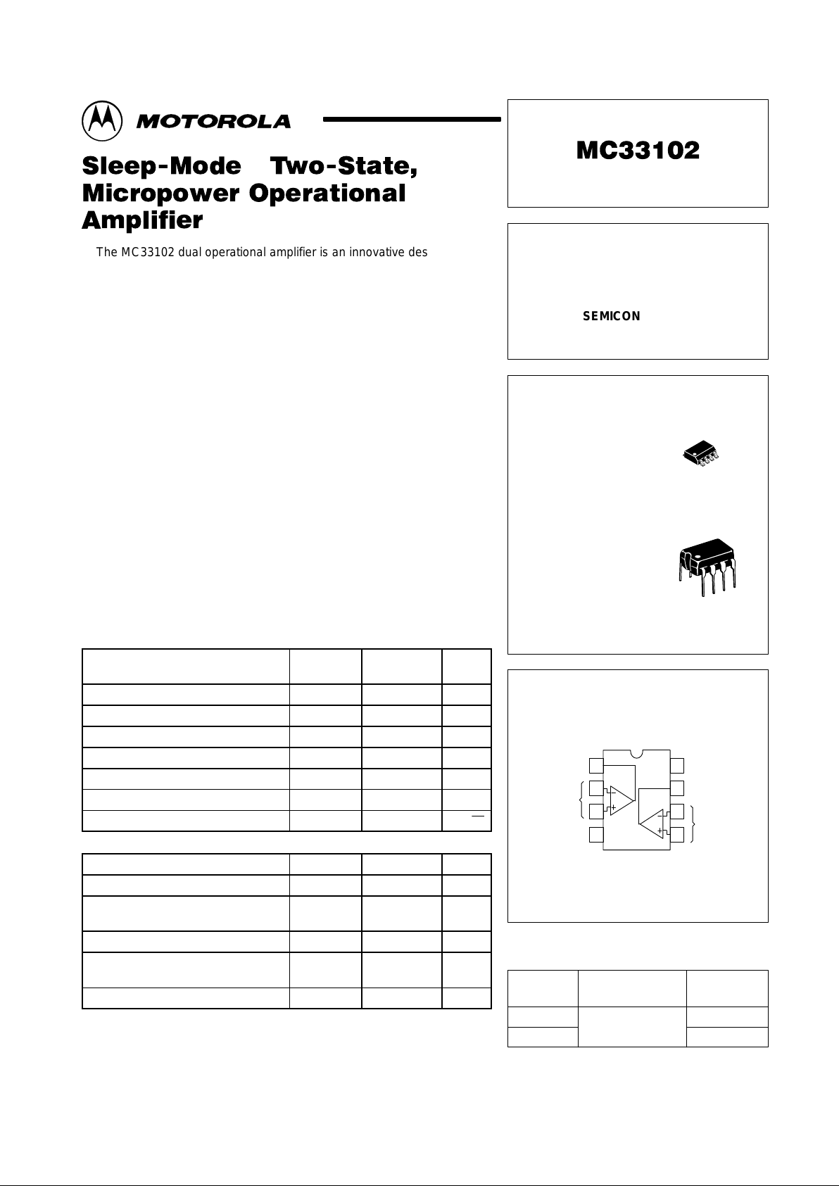
ORDERING INFORMATION
MC33102D
MC33102P
TA = – 40° to +85°C
SO–8
Plastic DIP
Order this document by MC33102/D
D SUFFIX
PLASTIC PACKAGE
CASE 751
(SO–8)
P SUFFIX
PLASTIC PACKAGE
CASE 626
8
1
1Output 1 V
CC
Output 2
PIN CONNECTIONS
(Dual, Top View)
8
1
Inputs 1
V
EE
Inputs
2
2
3
4
1
2
5
6
7
8
1
MOTOROLA ANALOG IC DEVICE DATA
The MC33102 dual operational amplifier is an innovative design concept
employing Sleep–Mode technology. Sleep–Mode amplifiers have two
separate states, a sleepmode and an awakemode. In sleepmode, the
amplifier is active and waiting for an input signal. When a signal is applied
causing the amplifier to source or sink 160 µA (typically) to the load, it will
automatically switch to the awakemode which offers higher slew rate, gain
bandwidth, and drive capability.
• Two States: “Sleepmode” (Micropower) and “Awakemode”
(High Performance)
• Switches from Sleepmode to Awakemode in 4.0 µs when Output Current
Exceeds the Threshold Current (RL = 600 Ω)
• Independent Sleepmode Function for Each Op Amp
• Standard Pinouts – No Additional Pins or Components Required
• Sleepmode State – Can Be Used in the Low Current Idle State as a
Fully Functional Micropower Amplifier
• Automatic Return to Sleepmode when Output Current Drops Below
Threshold
• No Deadband/Crossover Distortion; as Low as 1.0 Hz in the Awakemode
• Drop–in Replacement for Many Other Dual Op Amps
• ESD Clamps on Inputs Increase Reliability without Affecting Device
Operation
Sleep–Mode is a trademark of Motorola, Inc.
TYPICAL SLEEPMODE/AWAKEMODE PERFORMANCE
Characteristic
Sleepmode
(Typical)
Awakemode
(Typical) Unit
Low Current Drain 45 750 µA
Low Input Offset Voltage 0.15 0.15 mV
High Output Current Capability 0.15 50 mA
Low T.C. of Input Offset Voltage 1.0 1.0 µV/°C
High Gain Bandwidth (@ 20 kHz) 0.33 4.6 MHz
High Slew Rate 0.16 1.7 V/µs
Low Noise (@ 1.0 kHz) 28 9.0
nV/ Hz√
MAXIMUM RATINGS
Ratings Symbol Value Unit
Supply Voltage (VCC to VEE) V
S
+36 V
Input Differential Voltage Range
Input Voltage Range
V
IDR
V
IR
(Note 1) V
Output Short Circuit Duration (Note 2) t
SC
(Note 2) sec
Maximum Junction Temperature
Storage Temperature
T
J
T
stg
+150
–65 to +150
°C
Maximum Power Dissipation P
D
(Note 2) mW
NOTES: 1. Either or both input voltages should not exceed VCC or VEE.
2.Power dissipation must be considered to ensure maximum junction temperature (TJ)
is not exceeded (refer to Figure 1).
Motorola, Inc. 1996 Rev 0
Page 2
MC33102
2
MOTOROLA ANALOG IC DEVICE DATA
Simplified Block Diagram
Fractional
Load Current
Detector
% of I
L
Current
Threshold
Detector
Awake to
Sleepmode
Delay Circuit
Buffer Buffer
I
ref
C
Storage
I
Hysteresis
I
Enable
Enable
I
awake
Sleepmode
Current
Regulator
Awakemode
Current
Regulator
I
sleep
V
in
I
L
V
out
R
L
I
Bias
Op Amp
DC ELECTRICAL CHARACTERISTICS (V
CC
= +15 V , VEE = –15 V , TA = 25°C, unless otherwise noted.)
Characteristics
Figure Symbol Min Typ Max Unit
Input Offset Voltage (RS = 50 Ω, VCM = 0 V, VO = 0 V)
Sleepmode
TA = +25°C
TA = –40° to +85°C
Awakemode
TA = +25°C
TA = –40° to +85°C
2 VIO
—
—
—
—
0.15
—
0.15
—
2.0
3.0
2.0
3.0
mV
Input Offset Voltage Temperature Coefficient
(RS = 50 Ω, VCM = 0 V, VO = 0 V)
TA = –40° to +85°C (Sleepmode and Awakemode)
3 ∆VIO/∆T
— 1.0 —
µV/°C
Input Bias Current (VCM = 0 V, VO = 0 V)
Sleepmode
TA = +25°C
TA = –40° to +85°C
Awakemode
TA = +25°C
TA = –40° to +85°C
4, 6 I
IB
—
—
—
—
8.0
—
100
—
50
60
500
600
nA
Input Offset Current (VCM = 0 V, VO = 0 V)
Sleepmode
TA = +25°C
TA = –40° to +85°C
Awakemode
TA = +25°C
TA = –40° to +85°C
— IIO
—
—
—
—
0.5
—
5.0
—
5.0
6.0
50
60
nA
Page 3
MC33102
3
MOTOROLA ANALOG IC DEVICE DATA
DC ELECTRICAL CHARACTERISTICS (V
CC
= +15 V , VEE = –15 V , TA = 25°C, unless otherwise noted.)
Characteristics
Figure Symbol Min Typ Max Unit
Common Mode Input Voltage Range
(∆VIO = 5.0 mV, VO = 0 V)
Sleepmode and Awakemode
5 V
ICR
–13
—
–14.8
+14.2
—
+13
V
Large Signal Voltage Gain
Sleepmode (RL = 1.0 MΩ)
TA = +25°C
TA = –40° to +85°C
Awakemode (VO = ±10 V, RL = 600 Ω)
TA = +25°C
TA = –40° to +85°C
7 A
VOL
25
15
50
25
200
—
700
—
—
—
—
—
kV/V
Output Voltage Swing (VID = ±1.0 V)
Sleepmode (VCC = +15 V , VEE = –15 V)
RL = 1.0 MΩ
RL = 1.0 MΩ
Awakemode (VCC = +15 V , VEE = –15 V)
RL = 600 Ω
RL = 600 Ω
RL = 2.0 kΩ
RL = 2.0 kΩ
Awakemode (VCC = +2.5 V , VEE = –2.5 V)
RL = 600 Ω
RL = 600 Ω
8, 9, 10
V
O+
V
O–
V
O+
V
O–
V
O+
V
O–
V
O+
V
O–
+13.5
—
+12.5
—
+13.3
—
+1.1
—
+14.2
–14.2
+13.6
–13.6
+14
–14
+1.6
–1.6
—
–13.5
—
–12.5
—
–13.3
—
–1.1
V
V
Common Mode Rejection (VCM = ±13 V)
Sleepmode and Awakemode
11 CMR
80 90 —
dB
Power Supply Rejection (VCC/VEE = +15 V/–15 V ,
5.0 V/–15 V , +15 V/–5.0 V)
Sleepmode and Awakemode
12 PSR
80 100 —
dB
Output Transition Current
Sleepmode to Awakemode (Source/Sink)
(VS = ±15 V)
(VS = ±2.5 V)
Awakemode to Sleepmode (Source/Sink)
(VS = ±15 V)
(VS = ±2.5 V)
13, 14
I
TH1
I
TH2
200
250
—
—
160
200
142
180
—
—
90
140
µA
Output Short Circuit Current (Awakemode)
(VID = ±1.0 V , Output to Ground)
Source
Sink
15, 16 ISC
50
50
110
110
—
—
mA
Power Supply Current (per Amplifier) (ACL = 1, VO = 0V)
Sleepmode (VS = ±15 V)
TA = +25°C
TA = –40° to +85°C
Sleepmode (VS = ±2.5 V)
TA = +25°C
TA = –40° to +85°C
Awakemode (VS = ±15 V)
TA = +25°C
TA = –40° to +85°C
17 I
D
—
—
—
—
—
—
45
48
38
42
750
800
65
70
65
—
800
900
µA
Page 4
MC33102
4
MOTOROLA ANALOG IC DEVICE DATA
AC ELECTRICAL CHARACTERISTICS
(V
CC
= +15 V , VEE = –15 V , TA = 25°C, unless otherwise noted.)
Characteristics
Figure Symbol Min Typ Max Unit
Slew Rate (Vin = –5.0 V to +5.0 V, CL = 50 pF, AV = 1.0)
Sleepmode (RL = 1.0 MΩ)
Awakemode (RL = 600 Ω)
18 SR
0.10
1.0
0.16
1.7
—
—
V/µs
Gain Bandwidth Product
Sleepmode (f = 10 kHz)
Awakemode (f = 20 kHz)
19 GBW
0.25
3.5
0.33
4.6
—
—
MHz
Sleepmode to Awakemode Transition T ime
(ACL = 0.1, Vin = 0 V to +5.0 V)
RL = 600 Ω
RL = 10 kΩ
20, 21 t
tr1
—
—
4.0
15
—
—
µs
Awakemode to Sleepmode Transition T ime 22 t
tr2
— 1.5 — sec
Unity Gain Frequency (Open Loop)
Sleepmode (RL = 100 kΩ, CL = 0 pF)
Awakemode (RL = 600 Ω, CL = 0 pF)
f
U
—
—
200
2500
—
—
kHz
Gain Margin
Sleepmode (RL = 100 kΩ, CL = 0 pF)
Awakemode (RL = 600 Ω, CL = 0 pF)
23, 25 A
M
—
—
13
12
—
—
dB
Phase Margin
Sleepmode (RL = 100 kΩ, CL = 0 pF)
Awakemode (RL = 600 Ω, CL = 0 pF)
24, 26 ∅
M
—
—
60
60
—
—
Degrees
Channel Separation (f = 100 Hz to 20 kHz)
Sleepmode and Awakemode
29 CS
— 120 —
dB
Power Bandwidth (Awakemode)
(VO = 10 Vpp, RL = 100 kΩ, THD ≤ 1%)
BW
P
— 20 —
kHz
Total Harmonic Distortion (VO = 2.0 Vpp, AV = 1.0)
Awakemode (RL = 600 Ω)
f = 1.0 kHz
f = 10 kHz
f = 20 kHz
30 THD
—
—
—
0.005
0.016
0.031
—
—
—
%
DC Output Impedance (VO = 0 V, AV = 10, IQ = 10 µA)
Sleepmode
Awakemode
31 R
O
—
—
1.0 k
96
—
—
Ω
Differential Input Resistance (VCM = 0 V)
Sleepmode
Awakemode
R
in
—
—
1.3
0.17
—
—
MΩ
Differential Input Capacitance (VCM = 0 V)
Sleepmode
Awakemode
C
in
—
—
0.4
4.0
—
—
pF
Equivalent Input Noise Voltage (f = 1.0 kHz, RS = 100 Ω)
Sleepmode
Awakemode
32 e
n
—
—
28
9.0
—
—
nV/ Hz√
Equivalent Input Noise Current (f = 1.0 kHz)
Sleepmode
Awakemode
33 i
n
—
—
0.01
0.05
—
—
pA/ Hz√
Page 5
MC33102
5
MOTOROLA ANALOG IC DEVICE DATA
Sleepmode
Awakemode
VCC = +15 V
VEE = –15 V
TA = 25
°
C
TA, AMBIENT TEMPERATURE (°C)
10.0
, SLEEPMODE INPUT BIAS CURRENT (nA)
IB
I
8.0
6.0
4.0
2.0
0
, AWAKEMODE INPUT BIAS CURRENT (nA)
IB
I
, AWAKEMODE INPUT BIAS CURRENT (nA)
IB
I
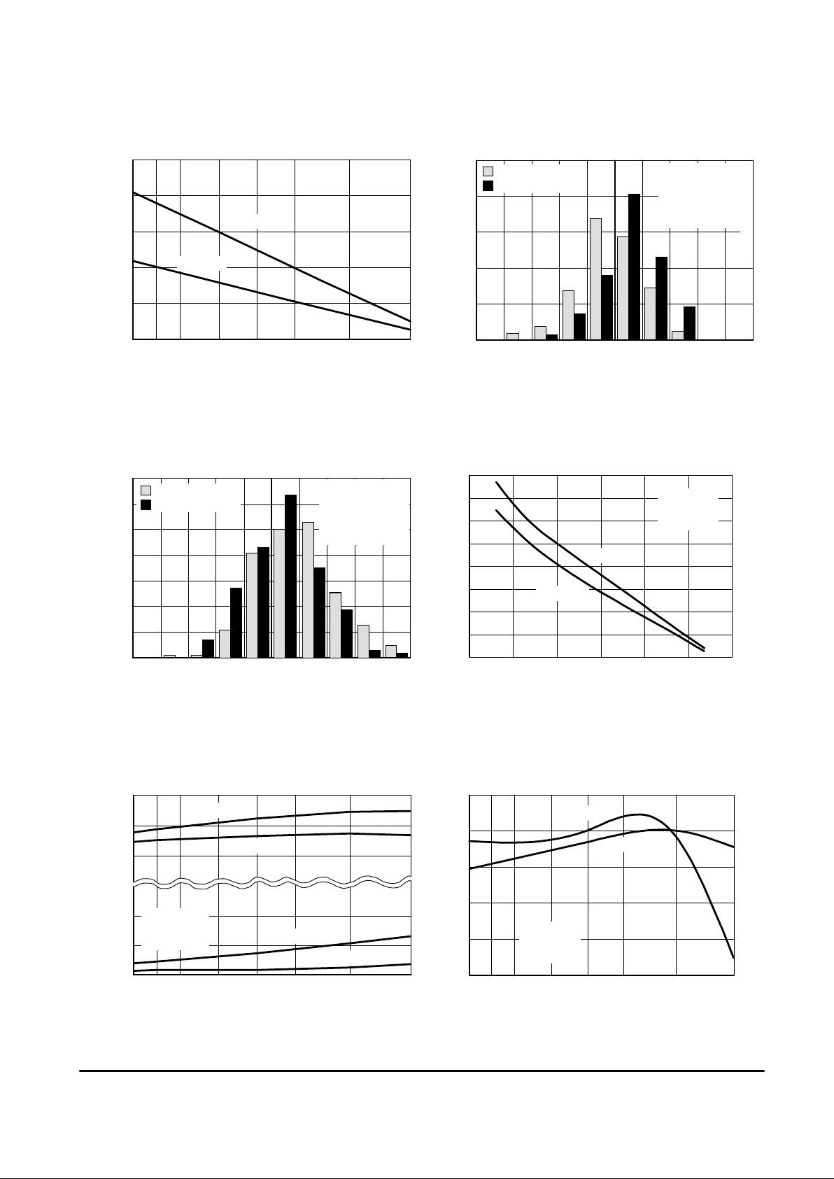
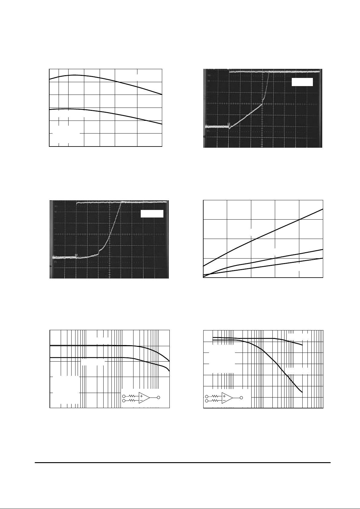
Figure 1. Maximum Power Dissipation
versus Temperature
, MAXIMUM POWER DISSIPATION (mW)
D(max)
P
TA, AMBIENT TEMPERATURE (°C)
2500
PERCENT OF AMPLIFIERS (%)
VIO, INPUT OFFSET VOLTAGE (mV)
50
PERCENT OF AMPLIFIERS (%)
TCVIO, INPUT OFFSET VOLTAGE TEMPERATURE COEFFICIENT (µV/°C)
35
, SLEEPMODE INPUT BIAS CURRENT (nA)
IB
I
VCM, COMMON MODE INPUT VOLTAGE (V)
10.5
, INPUT COMMON MODE VOL TAGE RANGE (V)
ICR
V
TA, AMBIENT TEMPERATURE (°C)
V
CC
2000
1500
1000
500
0
40
30
20
10
0
30
25
20
15
10
5.0
0
9.5
8.5
7.5
6.5
100
VCC–0.5
VCC–1.0
VEE+1.0
VEE+0.5
V
EE
–55 –25 0 25 50 85 125–40
–1.0
–5.0 –15 –10 –5.0 0 5.0 1510
–55 –25 0 25 50 85 125
–0.8 –0.6 –0.4 –0.2 0 0.2 0.4 0.6 0.8 1.0
–4.0 –3.0 –2.0 –1.0 0 1.0 2.0 3.0 4.0 5.0
–40
–55 –25 0 25 50 12585–40
MC33102P
MC33102D
204 Amplifiers tested
from 3 wafer lots.
VCC = +15 V
VEE = –15 V
TA = 25
°
C
Percent Sleepmode
Percent Awakemode
Figure 2. Distribution of Input Offset Voltage
(MC33102D Package)
Figure 3. Input Offset Voltage Temperature
Coefficient Distribution (MC33102D Package)
Percent Sleepmode
Percent Awakemode
204 Amplifiers tested
from 3 wafer lots.
VCC = +15 V
VEE = –15 V
TA = –40
°
C to 85°C
100
80
60
40
20
0
90
80
70
60
VCC = +15 V
VEE = –15 V
∆
VIO = 5.0 mV
VCC = +15 V
VEE = –15 V
VCM = 0 V
Awakemode
Awakemode
Awakemode
Sleepmode
Sleepmode
Sleepmode
Figure 4. Input Bias Current versus
Common Mode Input Voltage
Figure 5. Input Common Mode Voltage Range
versus Temperature
Figure 6. Input Bias Current versus Temperature
Page 6

MC33102
6
MOTOROLA ANALOG IC DEVICE DATA
V
O
, OUTPUT VOLT AGE (V )
pp
V
O
, OUTPUT VOLTAGE (V )
pp
, OPEN LOOP VOL TAGE GAIN (dB)
VOL
A
TA, AMBIENT TEMPERATURE (°C)
130
VCC, VEE
, SUPPLY VOLTAGE (V)
35
f, FREQUENCY (Hz)
30
RL, LOAD RESISTANCE T O GROUND (
Ω
)
30
CMR, COMMON MODE REJECTION (dB)
100 120
120
110
100
90
80
30
25
20
15
10
5
0
25
20
15
10
5.0
0
, OUTPUT VOLTAGE SWING (Vpp)
O
V
25
20
15
10
80
60
40
20
0
f, FREQUENCY (Hz)
PSR, POWER SUPPLY REJECTION (dB)
100
80
60
40
20
0
f, FREQUENCY (Hz)
Figure 7. Open Loop Voltage Gain
versus Temperature
–55 –25 0 25 50 85 125
0 3.0 6.0 9.0 12 1815
100 10
10
–40
1.0 k 10 k 100 k 500 k
5.0
100 1.0 k 10 k
100 1.0 k 10 k 100 k 1.0 M 10 100 1.0 k 10 k 100 k 1.0 M
Sleepmode (RL = 1.0 MΩ)
Awakemode (RL = 1.0 MΩ)
Figure 8. Output Voltage Swing
versus Supply Voltage
Awakemode (RL = 600 Ω)
Sleepmode (RL = 1.0 MΩ)
TA = 25°C
Figure 9. Output Voltage versus Frequency
VCC = +15 V
VEE = –15 V
AV = +1.0
TA = 25
°
C
Awakemode
(RL = 600
Ω
)
Sleepmode
(RL = 1.0 M
Ω
)
Figure 10. Maximum Peak–to–Peak Output
Voltage Swing versus Load Resistance
Awakemode
VCC = +15 V
VEE = –15 V
f = 1.0 kHz
TA = 25
°
C
Figure 11. Common Mode Rejection
versus Frequency
Awakemode
Sleepmode
VCC = +15 V
VEE = –15 V
VCM = 0 V
∆
VCM = ±1.5 V
TA = 25
°
C
+PSR
Awakemode
–PSR
Awakemode
+PSR
Sleepmode
–PSR
Sleepmode
Figure 12. Power Supply Rejection
versus Frequency
VCC = +15 V
VEE = –15 V
∆
VCC = ±1.5 V
TA = 25
°
C
Page 7

MC33102
7
MOTOROLA ANALOG IC DEVICE DATA
, OUTPUT SHORT CIRCUIT CURRENT (mA)
SC
I
, CURRENT THRESHOLD ( A)
TH1
I
, OUTPUT SHORT CIRCUIT CURRENT (mA)
SC
I
TA, AMBIENT TEMPERATURE (°C)
, SUPPLY CURRENT PER AMPLIFIER ( A)
D
I
TA, AMBIENT TEMPERATURE (°C)
, SLEW RATE (V/ s)
µ
TA, AMBIENT TEMPERATURE (°C)
VCC, VEE
, SUPPLY VOLTAGE (V)
µ
VCC, VEE
, SUPPLY VOLTAGE (V)
VO
, OUTPUT VOLTAGE (V)
µ
, SUPPLY CURRENT PER AMPLIFIER (mA)
D
I
SR
SLEW RATE (V/ s)
µ
SR,
Figure 13. Sleepmode to Awakemode
Current Threshold versus Supply Voltage
200
190
120 150
60 0.20
190
180
170
160
150
140
180
170
160
150
140
130
120
100
80
60
40
20
0
140
130
120
100
90
80
70
110
55
50
45
40
35
30
0.18
0.16
0.14
0.12
0.10
–55 –25 0 25 50 85 125
–55 –25 0 25 50 85 125 –55 –25 0 25 50 85 125
3.0 6.0 9.0 12 1815 3.0 6.0 9.0 12 1815
0 3.0 6.0 9.0 12 15 –40
–40 –40
1.2
1.0
0.8
0.6
0.4
2.0
1.8
1.6
1.4
1.2
1.0
0.2
0
, CURRENT THRESHOLD ( A)
TH2
I
µ
TA = 25°C
TA = –55°C
TA = 125°C
TA = 25°C
TA = –55°C
TA = 125°C
Source
Sink
VCC = +15 V
VEE = –15 V
VID =
±
1.0 V
RL < 10
Ω
Awakemode
Source
Sink
VCC = +15 V
VEE = –15 V
VID =
±
1.0 V
RL < 10
Ω
Awakemode
Sleepmode (µA)
Awakemode (mA)
VCC = +15 V
VEE = –15 V
No Load
VCC = +15 V
VEE = –15 V
∆
Vin = –5.0 V to +5.0 V
Awakemode (RL = 600 Ω)
Sleepmode (RL = 1.0 MΩ)
Figure 14. Awakemode to Sleepmode
Current Threshold versus Supply Voltage
Figure 15. Output Short Circuit Current
versus Output Voltage
Figure 16. Output Short Circuit Current
versus Temperature
Figure 17. Power Supply Current Per Amplifier
versus Temperature
Figure 18. Slew Rate versus Temperature
Page 8
MC33102
8
MOTOROLA ANALOG IC DEVICE DATA
V
O
R1
R2
Sleepmode
Awakemode
VCC = +15 V
VEE = –15 V
RT = R1 + R2
VO = 0 V
TA = 25
°
C
GBW, GAIN BANDWIDTH PRODUCT (KHz)
TA, AMBIENT TEMPERATURE (°C)
350
, TRANSITION TIME (SEC)
tr2
t
2.0
0
1.5
1.0
0.5
, GAIN MARGIN (dB)
m
A
15
, PHASE MARGIN (DEG)
m
∅
70
300
250
200
5.0
4.5
4.0
3.5
VCC,
VEE
, SUPPLY VOLTAGE (V)
13
11
9.0
7.0
5.0
RT, DIFFERENTIAL SOURCE RESISTANCE (
Ω
)
60
50
40
30
20
10
0
RT, DIFFERENTIAL SOURCE RESISTANCE (
Ω
)
GBW, GAIN BANDWIDTH PRODUCT (KHz)
V
O
R1
R2
t, TIME (5.0 µs/DIV)
, PEAK VOLTAGE (1.0 V/DIV)
P
V
RL = 10 k
, PEAK VOLTAGE (1.0 V/DIV)
P
V
t, TIME (2.0 µs/DIV)
RL = 600
Ω
Figure 19. Gain Bandwidth Product
versus Temperature
–55 –25 0 25 50 85 125–40
3.0 6.0 9.0 12 1815
10 100 1.0 k 10 k 10 100 1.0 k 10 k 100 k
Sleepmode (kHz)
Awakemode (MHz)
VCC = +15 V
VEE = –15 V
f = 20 kHz
Figure 20. Sleepmode to Awakemode
Transition Time
Figure 21. Sleepmode to Awakemode
Transition Time
Figure 22. Awakemode to Sleepmode
Transition Time versus Supply Voltage
TA = 25°C
TA = –55°C
TA = 125°C
Figure 23. Gain Margin versus Differential
Source Resistance
Figure 24. Phase Margin versus Differential
Source Resistance
Sleepmode
Awakemode
VCC = +15 V
VEE = –15 V
RT = R1 + R2
VO = 0 V
TA = 25
°
C
Page 9

MC33102
9
MOTOROLA ANALOG IC DEVICE DATA
2A
1B
2B
1A
1A) Phase, VS = ±18 V
2A) Phase, VS =
±
2.5 V
1B) Gain, VS =
±
18 V
2B) Gain, VS =
±
2.5 V
TA = 25°C
RL = 600
Ω
CL < 10 pF
Awakemode
CL, OUTPUT LOAD CAPACITANCE (pF)
14
f, FREQUENCY (Hz)
70
CS, CHANNEL SEPARATION (dB)
140
THD, TOT AL HARMONIC DISTORTION (%)
100
, OPEN LOOP GAIN MARGIN (dB)
m
A
, PHASE MARGIN (DEGREES)
m
∅
12
10
8.0
6.0
4.0
2.0
0
CL, OUTPUT LOAD CAPACITANCE (pF)
70
60
50
40
30
20
10
0
, VOLTAGE GAIN (dB)
V
A
50
30
10
–10
–30
1A
2A
1B
2B
, EXCESS PHASE (DEGREES)
θ
, VOLTAGE GAIN (dB)
V
A
70
50
30
10
–10
–30
f, FREQUENCY (Hz)
, EXCESS PHASE (DEGREES)
θ
120
100
80
60
40
20
0
f, FREQUENCY (Hz)
10
1.0
0.1
0.01
0.001
f, FREQUENCY (Hz)
Figure 25. Open Loop Gain Margin versus
Output Load Capacitance
10
10 k
100 1.0 k 10 100 1.0 k 10 k
100 k 1.0 M 10 M 30 k 100 k 1.0 M 10 M
100 1.0 k 10 k 100 k 100 1.0 k 10 k 100 k
Sleepmode
Awakemode
VCC = +15 V
VEE = –15 V
VO = 0 V
Sleepmode
Awakemode
VCC = +15 V
VEE = –15 V
VO = 0 V
Figure 26. Phase Margin versus
Output Load Capacitance
Figure 27. Sleepmode Voltage Gain and Phase
versus Frequency
1A) Phase, VS = ±18 V
2A) Phase, VS =
±
2.5 V
1B) Gain, VS =
±
18 V
2B) Gain, VS =
±
2.5 V
TA = 25°C
RL = 1.0 M
Ω
CL < 10 pF
Sleepmode
160
200
240
120
160
200
240
80
120
40
40
80
Figure 28. Awakemode Voltage Gain and
Phase versus Frequency
Figure 29. Channel Separation versus Frequency
VCC = +15 V
VEE = –15 V
RL = 600
Ω
Awakemode
VCC = +15 V
VEE = –15 V
RL = 600
Ω
VO = 2.0 Vpp
TA = 25
°
C
Awakemode
AV = +1000
AV = +100
AV = +10
AV = +1.0
Figure 30. Total Harmonic Distortion
versus Frequency
Page 10

MC33102
10
MOTOROLA ANALOG IC DEVICE DATA
, OUTPUT IMPEDANCE ( )
O
Z
250
e , INPUT REFERRED NOISE VOLTAGE (nV/ Hz)
100
1.0
os, PERCENT OVERSHOOT (%)
CL, LOAD CAPACITANCE (pF)
70
Ω
200
150
100
50
0
f, FREQUENCY (Hz)
50
10
5.0
f, FREQUENCY (Hz)
0.8
0.6
0.4
0.2
0.1
i , INPUT NOISE CURRENT (pA/ Hz)
f, FREQUENCY (Hz)
60
50
40
30
20
10
0
n
n
V
O
RS
V
O
, PEAK VOLTAGE (5.0 V/DIV)
P
V
t, TIME (50 µs/DIV)
RL =
R
, PEAK VOLTAGE (5.0 V/DIV)
P
V
t, TIME (5.0 µs/DIV)
RL = 600
Ω
Figure 31. Awakemode Output Impedance
versus Frequency
10
1.0 k 10 k 1.0 M 10 M100 k
10 100 10 k 100 k1.0 k
10 100 10 k 100 k1.0 k 100 1.0 k
VCC = +15 V
VEE = –15 V
VCM = 0 V
VO = 0 V
TA = 25
°
C
Awakemode
AV = 1000
AV = 10
AV = 1.0
AV = 100
Figure 32. Input Referred Noise Voltage
versus Frequency
Sleepmode
Awakemode
VCC = +15 V
VEE = –15 V
TA = 25
°
C
Figure 33. Current Noise versus Frequency
VCC = +15 V
VEE = –15 V
TA = 25
°
C
(RS = 10 k)
Awakemode
Sleepmode
Figure 34. Percent Overshoot
versus Load Capacitance
VCC = +15 V
VEE = –15 V
TA = 25
°
C
Awakemode
(RL = 600
Ω
)
Sleepmode
(RL = 1.0 M
Ω
)
Figure 35. Sleepmode Large Signal
Transient Response
Figure 36. Awakemode Large Signal
Transient Response
Page 11

MC33102
11
MOTOROLA ANALOG IC DEVICE DATA
t, TIME (50 µs/DIV)
, PEAK VOLTAGE (50 mV/DIV)
P
V
t, TIME (50 µs/DIV)
RL = 600
Ω
CL = 0 pF
, PEAK VOLTAGE (50 mV/DIV)
P
V
RL =
R
CL = 0 pF
Figure 37. Sleepmode Small Signal
Transient Response
Figure 38. Awakemode Small Signal
Transient Response
CIRCUIT INFORMATION
The MC33102 was designed primarily for applications
where high performance (which requires higher current drain)
is required only part of the time. The two–state feature of this
op amp enables it to conserve power during idle times, yet be
powered up and ready for an input signal. Possible
applications include laptop computers, automotive, cordless
phones, baby monitors, and battery operated test equipment.
Although most applications will require low power
consumption, this device can be used in any application
where better efficiency and higher performance is needed.
The Sleep–Mode amplifier has two states; a sleepmode
and an awakemode. In the sleepmode state, the amplifier is
active and functions as a typical micropower op amp. When a
signal is applied to the amplifier causing it to source or sink
sufficient current (see Figure 13), the amplifier will
automatically switch to the awakemode. See Figures 20 and
21 for transition times with 600 Ω and 10 kΩ loads.
The awakemode uses higher drain current to provide a
high slew rate, gain bandwidth, and output current capability .
In the awakemode, this amplifier can drive 27 Vpp into a
600 Ω load with VS = ±15 V.
An internal delay circuit is used to prevent the amplifier
from returning to the sleepmode at every zero crossing. This
delay circuit also eliminates the crossover distortion
commonly found in micropower amplifiers. This amplifier can
process frequencies as low as 1.0 Hz without the amplifier
returning to sleepmode, depending on the load.
The first stage PNP differential amplifier provides low noise
performance in both the sleep and awake modes, and an all
NPN output stage provides symmetrical source and sink AC
frequency response.
APPLICATIONS INFORMATION
The MC33102 will begin to function at power supply
voltages as low as VS = ±1.0 V at room temperature. (At this
voltage, the output voltage swing will be limited to a few
hundred millivolts.) The input voltages must range between
VCC and VEE supply voltages as shown in the maximum
rating table. Specifically, allowing the input to go more
negative than 0.3 V below VEE may cause product
damage. Also, exceeding the input common mode voltage
range on either input may cause phase reversal, even if the
inputs are between VCC and VEE.
When power is initially applied, the part may start to
operate in the awakemode. This is because of the currents
generated due to charging of internal capacitors. When this
occurs and the sleepmode state is desired, the user will have
to wait approximately 1.5 seconds before the device will
switch back to the sleepmode. T o prevent this from occurring,
ramp the power supplies from 1.0 V to full supply. Notice that
the device is more prone to switch into the awakemode when
VEE is adjusted than with a similar change in VCC.
The amplifier is designed to switch from sleepmode to
awakemode whenever the output current exceeds a preset
current threshold (ITH) of approximately 160 µA. As a result,
the output switching threshold voltage (VST) is controlled by
the output loading resistance (RL). This loading can be a load
resistor, feedback resistors, or both. Then:
VST = (160 µA) × R
L
Large valued load resistors require a large output voltage
to switch, but reduce unwanted transitions to the
awakemode. For instance, in cases where the amplifier is
connected with a large closed loop gain (ACL), the input offset
voltage (VIO) is multiplied by the gain at the output and could
produce an output voltage exceeding VST with no input
signal applied.
Small values of RL allow rapid transition to the awakemode
because most of the transition time is consumed slewing in
the sleepmode until VST is reached (see Figures 20, 21). The
output switching threshold voltage VST is higher for larger
values of RL, requiring the amplifier to slew longer in the
slower sleepmode state before switching to the awakemode.
Page 12

MC33102
12
MOTOROLA ANALOG IC DEVICE DATA
The transition time (t
tr1
) required to switch from sleep to
awake mode is:
t
tr1
t
D
I
TH
R
L
SR
sleepmode
= Sleepmode slew rate (0.16 V/µs)
= Amplifier delay (<1.0 µs)
= Output threshold current for
= more transition (160 µA)
= Load resistance
Where:
= tD = ITH (RL/SR
sleepmode
)
Although typically 160 µA, ITH varies with supply voltage
and temperature. In general, any current loading on the
output which causes a current greater than ITH to flow will
switch the amplifier into the awakemode. This includes
transition currents such as those generated by charging load
capacitances. In fact, the maximum capacitance that can be
driven while attempting to remain in the sleepmode is
approximately 1000 pF.
C
L(max)
= ITH/SR
sleepmode
= 160 µA/(0.16 V/µs)
= 1000 pF
Any electrical noise seen at the output of the MC33102
may also cause the device to transition to the awakemode. T o
minimize this problem, a resistor may be added in series with
the output of the device (inserted as close to the device as
possible) to isolate the op amp from both parasitic and load
capacitance.
The awakemode to sleepmode transition time is controlled
by an internal delay circuit, which is necessary to prevent the
amplifier from going to sleep during every zero crossing. This
time is a function of supply voltage and temperature as
shown in Figure 22.
Gain bandwidth product (GBW) in both modes is an
important system design consideration when using a
sleepmode amplifier. The amplifier has been designed to
obtain the maximum GBW in both modes. “Smooth” AC
transitions between modes with no noticeable change in the
amplitude of the output voltage waveform will occur as long
as the closed loop gains (ACL) in both modes are
substantially equal at the frequency of operation. For smooth
AC transitions:
(A
CLsleepmode
) (BW) < GBW
sleepmode
Where: A
CLsleepmode
= Closed loop gain in
A
CLsleepmode
= the sleepmode
BW = The required system bandwidth
BW = or operating frequency
TESTING INFORMATION
To determine if the MC33102 is in the awakemode or the
sleepmode, the power supply currents (ID+ and ID–) must be
measured. When the magnitude of either power supply
current exceeds 400 µA, the device is in the awakemode.
When the magnitudes of both supply currents are less than
400 µA, the device is in the sleepmode. Since the total supply
current is typically ten times higher in the awakemode than
the sleepmode, the two states are easily distinguishable.
The measured value of ID+ equals the ID of both devices
(for a dual op amp) plus the output source current of device A
and the output source current of device B. Similarly, the
measured value of ID– is equal to the ID– of both devices plus
the output sink current of each device. I
out
is the sum
of the currents caused by both the feedback loop and load
resistance. The total I
out
needs to be subtracted from the
measured ID to obtain the correct ID of the dual op amp.
An accurate way to measure the awakemode I
out
current
on automatic test equipment is to remove the I
out
current on
both Channel A and B. Then measure the ID values before
the device goes back to the sleepmode state. The transition
will take typically 1.5 seconds with ±15 V power supplies.
The large signal sleepmode testing in the characterization
was accomplished with a 1.0 MΩ load resistor which ensured
the device would remain in sleepmode despite large
voltage swings.
Page 13

MC33102
13
MOTOROLA ANALOG IC DEVICE DATA
D SUFFIX
PLASTIC PACKAGE
CASE 751–05
(SO–8)
ISSUE R
P SUFFIX
PLASTIC PACKAGE
CASE 626–05
ISSUE K
OUTLINE DIMENSIONS
NOTES:
1. DIMENSION L TO CENTER OF LEAD WHEN
FORMED PARALLEL.
2. PACKAGE CONTOUR OPTIONAL (ROUND OR
SQUARE CORNERS).
3. DIMENSIONING AND TOLERANCING PER ANSI
Y14.5M, 1982.
14
58
F
NOTE 2
–A–
–B–
–T–
SEATING
PLANE
H
J
G
D
K
N
C
L
M
M
A
M
0.13 (0.005) B
M
T
DIM MIN MAX MIN MAX
INCHESMILLIMETERS
A 9.40 10.16 0.370 0.400
B 6.10 6.60 0.240 0.260
C 3.94 4.45 0.155 0.175
D 0.38 0.51 0.015 0.020
F 1.02 1.78 0.040 0.070
G 2.54 BSC 0.100 BSC
H 0.76 1.27 0.030 0.050
J 0.20 0.30 0.008 0.012
K 2.92 3.43 0.115 0.135
L 7.62 BSC 0.300 BSC
M ––– 10 ––– 10
N 0.76 1.01 0.030 0.040
__
SEATING
PLANE
1
4
58
A0.25MCB
SS
0.25MB
M
h
q
C
X 45
_
L
DIM MIN MAX
MILLIMETERS
A 1.35 1.75
A1 0.10 0.25
B 0.35 0.49
C 0.18 0.25
D 4.80 5.00
E
1.27 BSCe
3.80 4.00
H 5.80 6.20
h
0 7
L 0.40 1.25
q
0.25 0.50
__
NOTES:
1. DIMENSIONING AND TOLERANCING PER ASME
Y14.5M, 1994.
2. DIMENSIONS ARE IN MILLIMETERS.
3. DIMENSION D AND E DO NOT INCLUDE MOLD
PROTRUSION.
4. MAXIMUM MOLD PROTRUSION 0.15 PER SIDE.
5. DIMENSION B DOES NOT INCLUDE MOLD
PROTRUSION. ALLOWABLE DAMBAR
PROTRUSION SHALL BE 0.127 TOTAL IN EXCESS
OF THE B DIMENSION AT MAXIMUM MATERIAL
CONDITION.
D
E
H
A
B
e
B
A1
C
A
0.10
Page 14

MC33102
14
MOTOROLA ANALOG IC DEVICE DATA
Motorola reserves the right to make changes without further notice to any products herein. Motorola makes no warranty , representation or guarantee regarding
the suitability of its products for any particular purpose, nor does Motorola assume any liability arising out of the application or use of any product or circuit, and
specifically disclaims any and all liability, including without limitation consequential or incidental damages. “T ypical” parameters which may be provided in Motorola
data sheets and/or specifications can and do vary in different applications and actual performance may vary over time. All operating parameters, including “Typicals”
must be validated for each customer application by customer’s technical experts. Motorola does not convey any license under its patent rights nor the rights of
others. Motorola products are not designed, intended, or authorized for use as components in systems intended for surgical implant into the body, or other
applications intended to support or sustain life, or for any other application in which the failure of the Motorola product could create a situation where personal injury
or death may occur. Should Buyer purchase or use Motorola products for any such unintended or unauthorized application, Buyer shall indemnify and hold Motorola
and its officers, employees, subsidiaries, affiliates, and distributors harmless against all claims, costs, damages, and expenses, and reasonable attorney fees
arising out of, directly or indirectly, any claim of personal injury or death associated with such unintended or unauthorized use, even if such claim alleges that Motorola
was negligent regarding the design or manufacture of the part. Motorola and are registered trademarks of Motorola, Inc. Motorola, Inc. is an Equal
Opportunity/Affirmative Action Employer.
Mfax is a trademark of Motorola, Inc.
How to reach us:
USA/EUROPE/Locations Not Listed: Motorola Literature Distribution; JAPAN: Nippon Motorola Ltd.: SPD, Strategic Planning Office, 4–32–1,
P.O. Box 5405, Denver, Colorado 80217. 1–303–675–2140 or 1–800–441–2447 Nishi–Gotanda, Shinagawa–ku, Tokyo 141, Japan. 81–3–5487–8488
Customer Focus Center: 1–800–521–6274
Mfax: RMFAX0@email.sps.mot.com – TOUCHTONE 1–602–244–6609 ASIA/PACIFIC: Motorola Semiconductors H.K. Ltd.; 8B Tai Ping Industrial Park,
Moto rola Fax Back Sys tem – US & Canada ONLY 1–800–774–1848 51 Ting Kok Road, Tai Po, N.T., Hong Kong. 852–26629298
– http://sps.motorola.com/mfax/
HOME PAGE: http://motorola.com/sps/
MC33102/D
◊
 Loading...