

Page 1
The MC33077 is a precision high quality, high frequency, low noise
monolithic dual operational amplifier employing innovative bipolar design
techniques. Precision matching coupled with a unique analog resistor trim
technique is used to obtain low input offset voltages. Dual–doublet frequency
compensation techniques are used to enhance the gain bandwidth product
of the amplifier. In addition, the MC33077 of fers low input noise voltage, low
temperature coefficient of input offset voltage, high slew rate, high AC and
DC open loop voltage gain and low supply current drain. The all NPN
transistor output stage exhibits no deadband cross–over distortion, large
output voltage swing, excellent phase and gain margins, low open loop
output impedance and symmetrical source and sink AC frequency
performance.
The MC33077 is tested over the automotive temperature range and is
available in plastic DIP and SO–8 packages (P and D suffixes).
• Low Voltage Noise: 4.4 nV/ Hz
• Low Input Offset V oltage: 0.2 mV
• Low TC of Input Offset V oltage: 2.0 µV/°C
• High Gain Bandwidth Product: 37 MHz @ 100 kHz
• High AC Voltage Gain: 370 @ 100 kHz
High AC Voltage Gain: 1850 @ 20 kHz
• Unity Gain Stable: with Capacitance Loads to 500 pF
• High Slew Rate: 1 1 V/µs
• Low Total Harmonic Distortion: 0.007%
• Large Output Voltage Swing: +14 V to –14.7 V
• High DC Open Loop Voltage Gain: 400 k (112 dB)
• High Common Mode Rejection: 107 dB
• Low Power Supply Drain Current: 3.5 mA
• Dual Supply Operation: ±2.5 V to ±18 V
Ǹ
@ 1.0 kHz
Order this document by MC33077/D
DUAL, LOW NOISE
OPERATIONAL AMPLIFIER
SEMICONDUCTOR
TECHNICAL DATA
8
1
P SUFFIX
PLASTIC PACKAGE
CASE 626
8
1
D SUFFIX
PLASTIC PACKAGE
CASE 751
(SO–8)
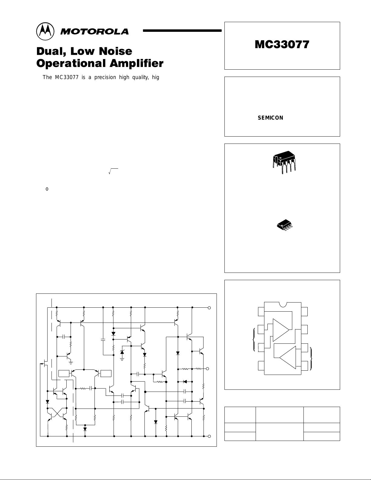
Representative Schematic Diagram (Each Amplifier)
R1 R6 R8 R11 R16
J
1
Q1
Q1
C1
Bias Network
Neg
Q2
Q4
D
1
Q5
R2
R3
Q6
R5
R4 R7
Q8
C2
D2
C3
PosQ7 Q9
D3
Q11
R9
Z1
Q12
Q10
R10 R12
MOTOROLA ANALOG IC DEVICE DATA
C6
Q13
Q14
D4
R13
R14
D5
Q16
R15
Q17
D6
R17 R18
D7
C7
C8
Q19
Q20
V
Q21
V
R19
Q22
R20
V
PIN CONNECTIONS
CC
out
Output 1
Inputs 1
1
–
2
4
V
EE
+
3
(Dual, Top View)
1
–
2
+
ORDERING INFORMATION
Operating
Device
MC33077D
MC33077P
EE
Motorola, Inc. 1996 Rev 0
Temperature Range
TA = – 40° to +85°C
8V
CC
7
Output 2
6
5
Package
SO–8
Plastic DIP
Inputs 2
1
Page 2
MC33077
MAXIMUM RATINGS
Rating Symbol Value Unit
Supply Voltage (VCC to VEE) V
Input Differential Voltage Range V
Input Voltage Range V
Output Short Circuit Duration (Note 2) t
Maximum Junction Temperature T
Storage Temperature T
Maximum Power Dissipation P
NOTES: 1. Either or both input voltages should not exceed VCC or VEE (See Applications Information).
2.Power dissipation must be considered to ensure maximum junction temperature (TJ) is not
exceeded (See power dissipation performance characteristic, Figure 1).
S
IDR
IR
SC
J
stg
D
+36 V
(Note 1) V
(Note 1) V
Indefinite sec
+150 °C
–60 to +150 °C
(Note 2) mW
DC ELECTRICAL CHARACTERISTICS (V
Characteristics Symbol Min Typ Max Unit
Input Offset Voltage (RS = 10 Ω, VCM = 0 V, VO = 0 V)
TA = +25°C
TA = –40° to +85°C
Average Temperature Coefficient of Input Offset Voltage
RS = 10 Ω, VCM = 0 V, VO = 0 V, TA = –40° to +85°C
Input Bias Current (VCM = 0 V, VO = 0 V)
TA = +25°C
TA = –40° to +85°C
Input Offset Current (VCM = 0 V, VO = 0 V)
TA = +25°C
TA = –40° to +85°C
Common Mode Input Voltage Range (∆VIO ,= 5.0 mV, VO = 0 V) V
Large Signal Voltage Gain (VO = ±1.0 V , RL = 2.0 kΩ)
TA = +25°C
TA = –40° to +85°C
Output Voltage Swing (VID = ±1.0 V)
RL = 2.0 kΩ
RL = 2.0 kΩ
RL = 10 kΩ
RL = 10 kΩ
Common Mode Rejection (Vin = ±13 V) CMR 85 107 — dB
Power Supply Rejection (Note 3)
VCC/VEE = +15 V/ –15 V to +5.0 V/ –5.0 V
Output Short Circuit Current (VID = ±1.0 V , Output to Ground)
Source
Sink
Power Supply Current (VO = 0 V, All Amplifiers)
TA = +25°C
TA = –40° to +85°C
NOTE: 3. Measured with VCC and VEE simultaneously varied.
= +15 V, VEE = –15 V, TA = 25°C, unless otherwise noted.)
CC
|VIO|
∆VIO/∆T — 2.0 — µV/°C
I
IB
I
IO
ICR
A
VOL
V
O+
V
O–
V
O+
V
O–
PSR 80 90 — dB
I
SC
I
D
±13.5 ±14 — V
150 k
125 k
+13.0
+13.4
—
—
—
—
—
—
—
—
+10
–20
—
—
0.13
—
280
—
15
—
400 k
—
+13.6
–14.1
+14.0
–14.7
+26
–33
3.5
—
1.0
1.5
1000
1200
180
240
—
—
—
–13.5
—
–14.3
+60
+60
4.5
4.8
mV
nA
nA
V/V
V
mA
mA
2
MOTOROLA ANALOG IC DEVICE DATA
Page 3
MC33077
AC ELECTRICAL CHARACTERISTICS (V
Characteristics Symbol Min Typ Max Unit
Slew Rate (Vin = –10 V to +10 V, RL = 2.0 kΩ, CL = 100 pF, AV = +1.0) SR 8.0 11 — V/µs
Gain Bandwidth Product (f = 100 kHz) GBW 25 37 — MHz
AC Voltage Gain (RL = 2.0 kΩ, VO = 0 V)
f = 100 kHz
f = 20 kHz
Unity Gain Frequency (Open Loop) f
Gain Margin (RL = 2.0 kΩ, CL = 10 pF) A
Phase Margin (RL = 2.0 kΩ, CL = 10 pF) ∅
Channel Separation (f = 20 Hz to 20 kHz, RL = 2.0 kΩ, VO = 10 Vpp) CS — –120 — dB
Power Bandwidth (VO = 27
Distortion (RL = 2.0 kΩ)
AV = +1.0, f = 20 Hz to 20 kHz
VO = 3.0 V
AV = 2000, f = 20 kHz
VO = 2.0 V
VO = 10 V
AV = 4000, f = 100 kHz
VO = 2.0 V
VO = 10 V
Open Loop Output Impedance (VO = 0 V, f = fU) |ZO| — 36 — Ω
Differential Input Resistance (VCM = 0 V) R
Differential Input Capacitance (VCM = 0 V) C
Equivalent Input Noise Voltage (RS = 100 Ω)
f = 10 Hz
f = 1.0 kHz
Equivalent Input Noise Current (f = 1.0 kHz)
f = 10 Hz
f = 1.0 kHz
rms
pp
pp
pp
pp
, RL = 2.0 kΩ, THD ≤ 1%) BW
p–p
= +15 V, VEE = –15 V, TA = 25°C, unless otherwise noted.)
CC
A
VO
U
m
m
p
THD
in
in
e
n
i
n
—
—
— 7.5 — MHz
— 10 — dB
— 55 —
— 200 — kHz
—
—
—
—
—
— 270 — kΩ
— 15 — pF
—
—
—
—
370
1850
0.007
0.215
0.242
0.3.19
0.316
6.7
4.4
1.3
0.6
—
—
Degrees
—
—
—
—
—
nV/ Hz√
—
—
pA/ Hz√
—
—
V/V
%
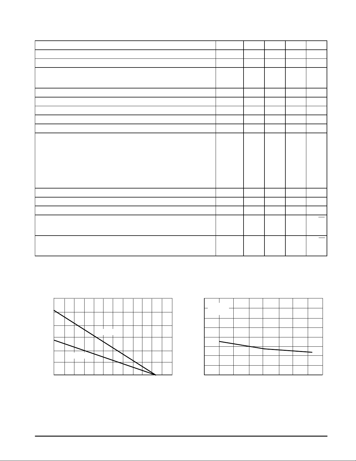
Figure 1. Maximum Power Dissipation
versus T emperature
2400
2000
1600
1200
800
, MAXIMUM POWER DISSIPATION (mW)
400
0
D(MAX)
P
–60 –40 –20 0 20 40 60 80 100 120 140 160 180
MC33077D
MC33077P
TA, AMBIENT TEMPERATURE (°C)
MOTOROLA ANALOG IC DEVICE DATA
Figure 2. Input Bias Current
versus Supply V oltage
800
VCM = 0 V
°
C
TA = 25
600
400
200
, INPUT BIAS CURRENT (nA)I
IB
0
0 2.5 5.0 7.5 10 12.5 15 17.5 20
VCC, |VEE|, SUPPLY VOLTAGE (V)
3
Page 4
MC33077
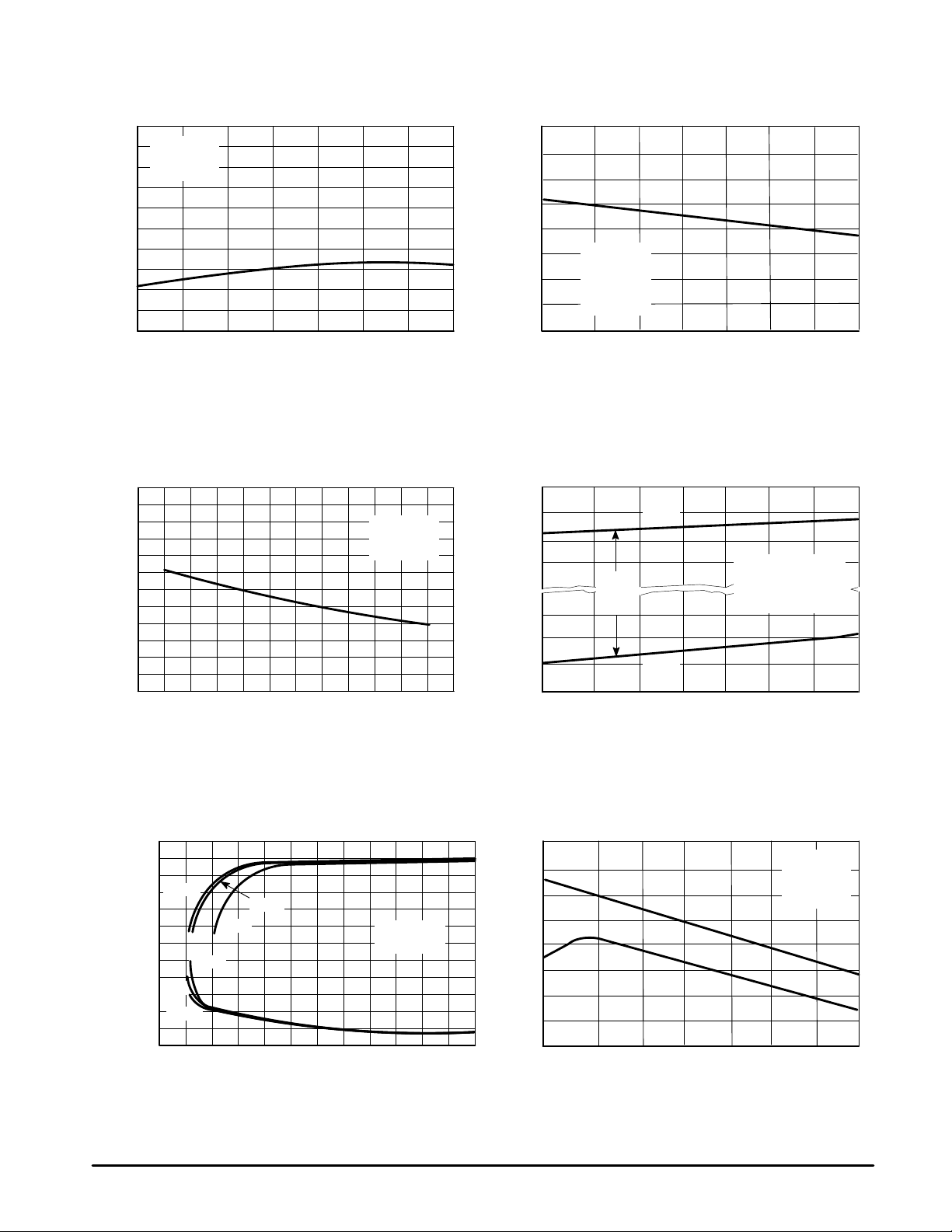
Figure 3. Input Bias Current
versus T emperature
1000
VCC = +15 V
VEE = –15 V
800
VCM = 0 V
600
400
, INPUT BIAS CURRENT (nA)I
200
IB
0
–55 –25 0 25 50 75 100 125 –55 –25 0 25 50 75 100 125
TA, AMBIENT TEMPERATURE (°C)
Figure 5. Input Bias Current versus
1.0
0.5
0
–0.5
IO
V , INPUT OFFSET VOLTAGE (mV)
–1.0
Figure 6. Input Common Mode V oltage Range
Common Mode V oltage
600
500
400
300
200
, INPUT BIAS CURRENT (nA)I
IB
100
0
–15 –10 –5.0 0 5.0 10 15
VCM, COMMON MODE VOLTAGE (V)
VCC = +15 V
VEE = –15 V
TA = 25
°
C
VCC 0.0
VCC –0.5
VCC –1.0
VCC –1.5
VEE +1.5
VEE +1.0
VEE +0.5
, INPUT COMMON MODE VOT AGE RANGE (V)
VEE +0.0
–55 –25 0 25 50 75 100 125
ICR
V
Figure 4. Input Offset Voltage
versus T emperature
VCC = +15 V
VEE = –15 V
Ω
RS = 10
VCM = 0 V
AV = +1.0
TA, AMBIENT TEMPERATURE (°C)
versus T emperature
+V
CM
VCC = +3.0 V to +15 V
Input
Voltage
Range
–V
CM
TA, AMBIENT TEMPERATURE (°C)
VEE = –3.0 V to –15 V
∆
VIO = 5.0 mV
VO = 0 V
sat
V , OUTPUT SATURA TION VOLTAGE (V)
4
Figure 7. Output Saturation Voltage versus
Load Resistance to Ground
VCC 0
VCC –2
–55°C
VCC –4
125°C
VEE +4
VEE +2
VEE 0
°
C
25
–55
°
C
0 0.5 1.0 1.5 2.0 2.5 3.0 –55 –25 0 25 50 75 100 125
25°C
125°C
RL, LOAD RESISTANCE T O GROUND (kΩ)
VCC = +15 V
VEE = –15 V
SC
|I |, OUTPUT SHOR T CIRCUIT CURRENT (mA)
50
40
30
20
10
Figure 8. Output Short Circuit Current
versus T emperature
Sink
Source
TA, AMBIENT TEMPERATURE (°C)
MOTOROLA ANALOG IC DEVICE DATA
VCC = +15 V
VEE = –15 V
±
1.0 V
VID =
Ω
RL < 100
Page 5

MC33077
Figure 9. Supply Current
versus T emperature
5.0
4.0
3.0
±
15 V
±
5.0 V
2.0
VCM = 0 V
∞
1.0
CC
I , SUPPLY CURRENT (mA)
0
–55 –25 0 25 50 75 100 125
RL =
VO = 0 V
TA, AMBIENT TEMPERATURE (°C)
Figure 11. Power Supply Rejection
versus Frequency
120
+PSR = 20Log
100
80
60
∆
∆
–PSR
VO/A
V
CC
DM
–PSR = 20Log
+PSR
∆
VO/A
∆
V
EE
DM
Figure 10. Common Mode Rejection
versus Frequency
120
–
100
80
∆
V
CM
CMR = 20Log
A
DM
+
∆
V
CM
×
∆
V
O
60
VCC = +15 V
40
VEE = –15 V
VCM = 0 V
∆
VCM = ±1.5 V
20
CMR, COMMON MODE REJECTION (dB)
0
100 1.0 k 10 k 100 k 1.0 M 10 M
TA = 25
°
C
f, FREQUENCY (Hz)
Figure 12. Gain Bandwidth Product
versus Supply V oltage
48
RL = 10 k
Ω
CL = 0 pF
44
f = 100 kHz
°
C
TA = 25
40
36
∆
V
O
A
DM
40
VCC = +15 V
20
VEE = –15 V
°
C
PSR, POWER SUPPLY REJECTION (dB)
TA = 25
0
100 1.0 k 10 k 100 k 1.0 M 0 5 10 15 20
V
CC
–
A
DM
+
∆
V
O
V
EE
f, FREQUENCY (Hz)
Figure 13. Gain Bandwidth Product
versus T emperature
50
VCC = +15 V
46
42
38
34
30
GBW, GAIN BANDWIDTH PRODUCT (MHz)
26
–55 –25 0 25 50 75 100 125
TA, AMBIENT TEMPERATURE (
VEE = –15 V
f = 100 kHz
RL = 10 k
CL = 0 pF
°
C)
Ω
32
28
GBW, GAIN BANDWIDTH PRODUCT (MHz)
24
VCC, |VEE|, SUPPLY VOLTAGE (V)
Figure 14. Maximum Output V oltage
versus Supply V oltage
20
TA = 25°C
15
p
10
Vp +
5.0
0
–5.0
,OUTPUT VOLTAGE (V )
–10
O
V
–15
–20
0 5.0 10 15 20
VCC, |VEE|, SUPPLY VOLTAGE (V)
RL = 10 k
Vp –
RL = 10 k
Ω
RL = 2.0 k
RL = 2.0 k
Ω
Ω
Ω
MOTOROLA ANALOG IC DEVICE DATA
5
Page 6

MC33077
Figure 15. Output Voltage
versus Frequency
30
25
pp
20
15
VCC = +15 V
VEE = –15 V
10
5.0
RL = 2.0 k
AV =+1.0
THD
, OUTPUT VOLTAGE (V )
O
V
TA = 25
0
100 1.0 k 10 k 100 k 1.0 M
≤
1.0%
°
Ω
C
f, FREQUENCY (Hz) VCC, |VEE|, SUPPLY VOLTAGE (V)
Figure 17. Open Loop V oltage Gain
versus T emperature
600
VCC = +15 V
550
500
450
400
350
OPEN LOOP VOLTAGE GAIN (X1000 V/V)A
,
300
VOL
–55 –25 0 25 50 75 100 125
TA, AMBIENT TEMPERATURE (°C)
VEE = –15 V
RL = 2.0 k
Ω
f = 10 Hz
∆
VO = –10 V to +10 V
Figure 16. Open Loop V oltage Gain
versus Supply V oltage
1200
RL = 2.0 k
Ω
f = 10 Hz
1000
∆
VO = 2/3 (VCC –VEE)
°
C
TA = 25
800
600
400
200
OPEN LOOP VOLTAGE GAIN (X1000 V/V)A
,
VOL
0
0 5.0 10 15 20
Figure 18. Output Impedance
versus Frequency
80
VCC = +15 V
70
Ω
O
| Z |, OUTPUT IMPEDANCE ( )
VEE = –15 V
VO = 0 V
60
TA = 25
°
C
50
40
30
20
AV = 1000
AV = 100
AV = 10
10
0
100 1.0 k 10 k 100 k 1.0 M 10 M
f, FREQUENCY (Hz)
AV = 1.0
Figure 19. Channel Separation
versus Frequency
160
150
140
∆
V
in
–
+
Measurement Channel
∆
V
O
Drive Channel
VCC = +15 V
VEE = –15 V
RL = 2.0 k
VOD = 20 V
∆
TA = 25
°
C
130
120
110
CS, CHANNEL SEPARATION (dB)
CS = 20 Log
100
10 100 1.0 k 10 k 100 k
f, FREQUENCY (Hz)
6
Figure 20. T otal Harmonic Distortion
versus Frequency
1.0
VCC = +15 V VO = 2.0 Vpp
VEE = –15 V TA = 25
°
C
AV = +1000
Ω
pp
0.1
AV = +100
AV = +10
2.0 k
100 k
0.01
∆
V
OD
∆
V
in
THD, TOT AL HARMONIC DISTORTION (%)
0.001
R
–
A
+
V
in
10 100 1.0 k 10 k 100 k
Ω
Ω
V
O
AV = +1.0
f, FREQUENCY (Hz)
MOTOROLA ANALOG IC DEVICE DATA
Page 7

MC33077
Figure 21. T otal Harmonic Distortion
versus Frequency
1.0
VCC = +15 V
VEE = –15 V
V0 = –10 Vpp
°
C
TA = 25
0.1
AV = +1000
AV = +100
0.01
AV = +10
AV = +1.0
THD, TOT AL HARMONIC DISTORTION (%)
0.001
10 100 1.0 k 10 k 100 k
100 k
Ω
2.0 k
Ω
R
–
A
+
V
in
V
O
1.0
0.5
0.1
0.05
0.01
0.005
THD, TOT AL HARMONIC DISTORTION (%)
0.001
Figure 22. T otal Harmonic Distortion
versus Output Voltage
VCC = +15 V
VEE = –15 V
f = 20 kHz
°
C
TA = 25
AV = +1000
AV = +100
AV = +10
AV = +1.0
0 2.0 4.0 6.0 8.0 10 12
f, FREQUENCY (Hz) VO, OUTPUT VOLTAGE (Vpp)
Figure 23. Slew Rate versus Supply V oltage Figure 24. Slew Rate versus T emperature
16
Vin = 2/3 (VCC –VEE)
°
C
TA = 25
12
µ
40
VCC = +15 V
VEE = –15 V
30
∆
µ
Vin = 20 V
∆
V
in
100 k
Ω
2.0 k
Ω
R
–
A
+
V
in
–
+
Ω
2.0 k
V
O
VO
100 pF
8.0
–
+
∆
V
4.0
SR, SLEW RATE (V/ s)
in
2.0 k
Ω
V
O
100 pF
0
0 2.5 5.0 7.5 10 12.5 15 17.5 20 –25 0 25 50 75 100 125–55
VCC, |VEE|, SUPPLY VOLTAGE (V)
Figure 25. V oltage Gain and Phase
versus Frequency
180
140
100
60
Phase
Gain
VCC = +15 V
VEE = –15 V
RL = 2.0 k
TA = 25°C
0
40
Ω
80
120
20
10
SR, SLEW RATE (V/ s)
0
TA, AMBIENT TEMPERATURE (°C)
Figure 26. Open Loop Gain Margin and Phase
Margin versus Output Load Capacitance
14
12
10
8.0
125°C
25°C
–55°C
–
V
+
in
2.0 k
Ω
C
V
O
L
6.0
OPEN–LOOP VOL TAGE GAIN (dB)A
,
VOL
20
–20
–60
160
, EXCESS PHASE (DEGREES)
200
φ
240
4.0
m
2.0
A , OPEN LOOP GAIN MARGIN (dB)
0
125°C
–55°C
25°C
VCC = +15 V
VEE = –15 V
VO = 0 V
10 100 1.0 k 10 k 100 k 1.0 M 10 M 100 M 1.0 10 100 1000
f, FREQUENCY (Hz)
CL, OUTPUT LOAD CAPACITANCE (pF)
Phase
Gain
0
10
20
30
40
50
, PHASE MARGIN (DEGREES)
m
φ
60
70
MOTOROLA ANALOG IC DEVICE DATA
7
Page 8
MC33077
Figure 27. Phase Margin versus
Output Voltage
70
60
50
CL = 0 pF
CL = 100 pF
40
VCC = +15 V
30
20
, PHASE MARGIN (DEGREES)
m
10
φ
0
–10 –5.0 0 5.0 10
VEE = –15 V
°
C
TA = 25
CL = 300 pF
CL = 500 pF
V
in
–
+
2.0k
Ω
VO, OUTPUT VOLTAGE (V)
Figure 29. Input Referred Noise V oltage
and Current versus Frequency
100
nV/ Hz√
50
30
20
VCC = +15 V
VEE = –15 V
°
TA = 25
Figure 28. Overshoot versus
Output Load Capacitance
100
80
–
+
∆
V
in
2.0 k
Ω
V
O
100 pF
60
40
os, OVERSHOOT (%)
V
O
C
L
20
125°C and 25°C
0
1 10 100 1000
CL, OUTPUT LOAD CAPACITANCE (pF)
VCC = +15 V
VEE = –15 V
∆
Vin = 100 mV
–55°C
Figure 30. T otal Input Referred Noise Voltage
versus Source Resistant
10
5.0
C
3.0
2.0
nV/ Hz√
1000
VCC = +15 V f = 1.0 kHz
VEE = –15 V TA = 25
Vn (total) =
100
Ǹ
(inRs)2)
°
C
2
e
)
4KTR
n
S
10
1.0
Current
5.0
3.0
Voltage
2.0
1.0
1.0 10 100 1.0 k 10 k 100 k 10 100 1.0 k 10 k 100 k 1.0 M
n
e , INPUT REFERRED NOISE VOL TAGE ( )
f, FREQUENCY (Hz)
0.5
0.3
0.2
0.1
n
i ,INPUT REFERRED NOISE CURRENT (pA)
10
1.0
n
V
V , TOTAL REFERRED NOISE VOL TAGE ( )
RS, SOURCE RESISTANCE (
Ω
)
Figure 31. Phase Margin and Gain Margin
versus Differential Source Resistance
14
12
R
10
8.0
V
in
1
R2
–
+
6.0
m
4.0
A , GAIN MARGIN (dB)
2.0
0
1.0 10 100 1.0 k 10 k
RT, DIFFERENTIAL SOURCE RESISTANCE (Ω)
Gain
V
O
Phase
VCC = +15 V
VEE = –15 V
RT = R1 + R
VO = 0 V
°
C
TA = 25
0
10
20
30
40
50
2
,PHASE MARGIN (DEGREES)
m
60
φ
70
Figure 32. Inverting Amplifer Slew Rate
VCC = +15 V
VEE = –15 V
AV = –1.0
RL = 2.0 k
CL = 100 pF
TA = 25
O
V , OUTPUT VOLTAGE (5.0 V/DIV)
Ω
°
C
t, TIME (2.0 µs/DIV)
8
MOTOROLA ANALOG IC DEVICE DATA
Page 9

MC33077
Figure 33. Noninverting Amplifier Slew Rate Figure 34. Noninverting Amplifier Overshoot
VCC = +15 V
VEE = –15 V
O
V , OUTPUT VOL TAGE (5.0 V/DIV)
AV = +1.0
RL = 2.0 k
CL = 100 pF
TA = 25
Ω
°
C
VCC = +15 V
VEE = –15 V
AV = +1.0
RL = 2.0 k
TA = 25°C
O
V , OUTPUT VOL TAGE (5.0 V/DIV)
t, TIME (2.0 µs/DIV) t, TIME (200 ns/DIV)
Ω
Figure 35. Low Frequency Noise V oltage
versus Time
CL = 100 pF
CL = 0 pF
n
e , INPUT NOISE VOL TAGE (100nV/DIV)
VCC = +15 V
VEE = –15 V
BW = 0.1 Hz to 10 Hz
°
C
TA = 25
See Noise Circuit
(Figure 36)
t, TIME (1.0 sec/DIV)
MOTOROLA ANALOG IC DEVICE DATA
9
Page 10

MC33077
APPLICATIONS INFORMATION
The MC33077 is designed primarily for its low noise, low
offset voltage, high gain bandwidth product and large output
swing characteristics. Its outstanding high frequency
gain/phase performance make it a very attractive amplifier for
high quality preamps, instrumentation amps, active filters
and other applications requiring precision quality
characteristics.
The MC33077 utilizes high frequency lateral PNP input
transistors in a low noise bipolar differential stage driving a
compensated Miller integration amplifier. Dual–doublet
frequency compensation techniques are used to enhance the
gain bandwidth product. The output stage uses an all NPN
transistor design which provides greater output voltage swing
and improved frequency performance over more
conventional stages by using both PNP and NPN transistors
(Class AB). This combination produces an amplifier with
superior characteristics.
Through precision component matching and innovative
current mirror design, a lower than normal temperature
coefficient of input offset voltage (2.0 µV/°C as opposed to 10
µV/°C), as well as low input offset voltage, is accomplished.
The minimum common mode input range is from 1.5 V
below the positive rail (VCC) to 1.5 V above the negative rail
(VEE). The inputs will typically common mode to within 1.0 V
of both negative and positive rails though degradation in
offset voltage and gain will be experienced as the common
mode voltage nears either supply rail. In practice, though not
recommended, the input voltage may exceed VCC by
approximately 30 V and decrease below the VEE by
approximately 0.6 V without causing permanent damage to
the device. If the input voltage on either or both inputs is less
than approximately 0.6 V, excessive current may flow, if not
limited, causing permanent damage to the device.
The amplifier will not latch with input source currents up to
20 mA, though in practice, source currents should be limited
to 5.0 mA to avoid any parametric damage to the device. If
both inputs exceed VCC, the output will be in the high state
and phase reversal may occur. No phase reversal will occur
if the voltage on one input is within the common mode range
and the voltage on the other input exceeds VCC. Phase
reversal may occur if the input voltage on either or both inputs
is less than 1.0 V above the negative rail. Phase reversal will
be experienced if the voltage on either or both inputs is less
than VEE.
Through the use of dual–doublet frequency compensation
techniques, the gain bandwidth product has been greatly
enhanced over other amplifiers using the conventional single
pole compensation. The phase and gain error of the amplifier
remains low to higher frequencies for fixed amplifier gain
configurations.
With the all NPN output stage, there is minimal swing loss
to the supply rails, producing superior output swing, no
crossover distortion and improved output phase symmetry
with output voltage excursions (output phase symmetry
being the amplifiers ability to maintain a constant phase
relation independent of its output voltage swing). Output
phase symmetry degradation in the more conventional PNP
and NPN transistor output stage was primarily due to the
inherent cut–off frequency mismatch of the PNP and NPN
transistors used (typically 10 MHz and 300 MHz,
respectively), causing considerable phase change to occur
as the output voltage changes. By eliminating the PNP in the
output, such phase change has been avoided and a very
significant improvement in output phase symmetry as well as
output swing has been accomplished.
The output swing improvement is most noticeable when
operation is with lower supply voltages (typically 30% with
± 5.0 V supplies). With a 10 k load, the output of the amplifier
can typically swing to within 1.0 V of the positive rail (VCC),
and to within 0.3 V of the negative rail (VEE), producing a 28.7
Vpp signal from ±15 V supplies. Output voltage swing can be
further improved by using an output pull–up resistor
referenced to the VCC. Where output signals are referenced
to the positive supply rail, the pull–up resistor will pull the
output to VCC during the positive swing, and during the
negative swing, the NPN output transistor collector will pull
the output very near VEE. This configuration will produce the
maximum attainable output signal from given supply
voltages. The value of load resistance used should be much
less than any feedback resistance to avoid excess loading
and allow easy pull–up of the output.
Output impedance of the amplifier is typically less than
50 Ω at frequencies less than the unity gain crossover
frequency (see Figure 18). The amplifier is unity gain stable
with output capacitance loads up to 500 pF at full output
swing over the –55° to +125°C temperature range. Output
phase symmetry is excellent with typically 4°C total phase
change over a 20 V output excursion at 25°C with a 2.0 kΩ
and 100 pF load. With a 2.0 kΩ resistive load and no
capacitance loading, the total phase change is approximately
one degree for the same 20 V output excursion. With a
2.0 kΩ and 500 pF load at 125°C, the total phase change is
typically only 10°C for a 20 V output excursion (see Figure
27).
As with all amplifiers, care should be exercised to insure
that one does not create a pole at the input of the amplifier
which is near the closed loop corner frequency. This
becomes a greater concern when using high frequency
amplifiers since it is very easy to create such a pole with
relatively small values of resistance on the inputs. If this does
10
MOTOROLA ANALOG IC DEVICE DATA
Page 11

MC33077
occur, the amplifier’s phase will degrade severely causing the
amplifier to become unstable. Effective source resistances,
acting in conjunction with the input capacitance of the
amplifier, should be kept to a minimum to avoid creating such
a pole at the input (see Figure 31). There is minimal effect on
stability where the created input pole is much greater than the
closed loop corner frequency. Where amplifier stability is
affected as a result of a negative feedback resistor in
conjunction with the amplifier’s input capacitance, creating a
pole near the closed loop corner frequency, lead capacitor
compensation techniques (lead capacitor in parallel with the
feedback resistor) can be employed to improve stability . The
feedback resistor and lead capacitor RC time constant
should be larger than that of the uncompensated input pole
frequency. Having a high resistance connected to the
noninverting input of the amplifier can create a like instability
problem. Compensation for this condition can be
accomplished by adding a lead capacitor in parallel with the
noninverting input resistor of such a value as to make the RC
time constant larger than the RC time constant of the
uncompensated input resistor acting in conjunction with the
amplifiers input capacitance.
For optimum frequency performance and stability, careful
component placement and printed circuit board layout should
be exercised. For example, long unshielded input or output
leads may result in unwanted input output coupling. In order
to reduce the input capacitance, the body of resistors
connected to the input pins should be physically close to the
input pins. This not only minimizes the input pole creation for
optimum frequency response, but also minimizes extraneous
signal “pickup” at this node. Power supplies should be
decoupled with adequate capacitance as close as possible to
the device supply pin.
In addition to amplifier stability considerations, input
source resistance values should be low to take full advantage
of the low noise characteristics of the amplifier. Thermal
noise (Johnson Noise) of a resistor is generated by
thermally–charged carriers randomly moving within the
resistor creating a voltage. The rms thermal noise voltage in
a resistor can be calculated from:
Enr =
/
4k TR × BW
where:
k = Boltzmann’s Constant (1.38 × 10
–23
joules/k)
T = Kelvin temperature
R = Resistance in ohms
BW = Upper and lower frequency limit in Hertz.
By way of reference, a 1.0 kΩ resistor at 25°C will produce
nV/ Hz√
a 4.0
of rms noise voltage. If this resistor is
connected to the input of the amplifier, the noise voltage will
be gained–up in accordance to the amplifier’s gain
configuration. For this reason, the selection of input source
resistance for low noise circuit applications warrants serious
consideration. The total noise of the amplifier, as referred to
its inputs, is typically only 4.4
nV/ Hz√
at 1.0 kHz.
The output of any one amplifier is current limited and thus
protected from a direct short to ground, However, under such
conditions, it is important not to allow the amplifier to exceed
the maximum junction temperature rating. Typically for ±15 V
supplies, any one output can be shorted continuously to
ground without exceeding the temperature rating.
Figure 36. V oltage Noise Test Circuit
0.1
µ
F
100 k
Ω
10
Note: All capacitors are non–polarized.
Ω
–
D.U.T.
+
Voltage Gain = 50,000
2.0 k
4.7 µF
Ω
(0.1 Hz to 10 Hz
Ω
24.3 k
)
p–p
+
1/2
MC33077
–
100 k
0.1 µF
µ
F
4.3 k
Ω
2.2
22
Ω
µ
F
Rin = 1.0 M
110 k
Ω
Scope
×
1
Ω
MOTOROLA ANALOG IC DEVICE DATA
11
Page 12
NOTE 2
A
E
B
C
A1
–T–
SEATING
PLANE
H
58
14
F
–A–
N
D
G
0.13 (0.005) B
D
58
1
H
4
e
A
B
SS
A0.25MCB
–B–
C
K
M
T
0.25MB
SEATING
PLANE
0.10
MC33077
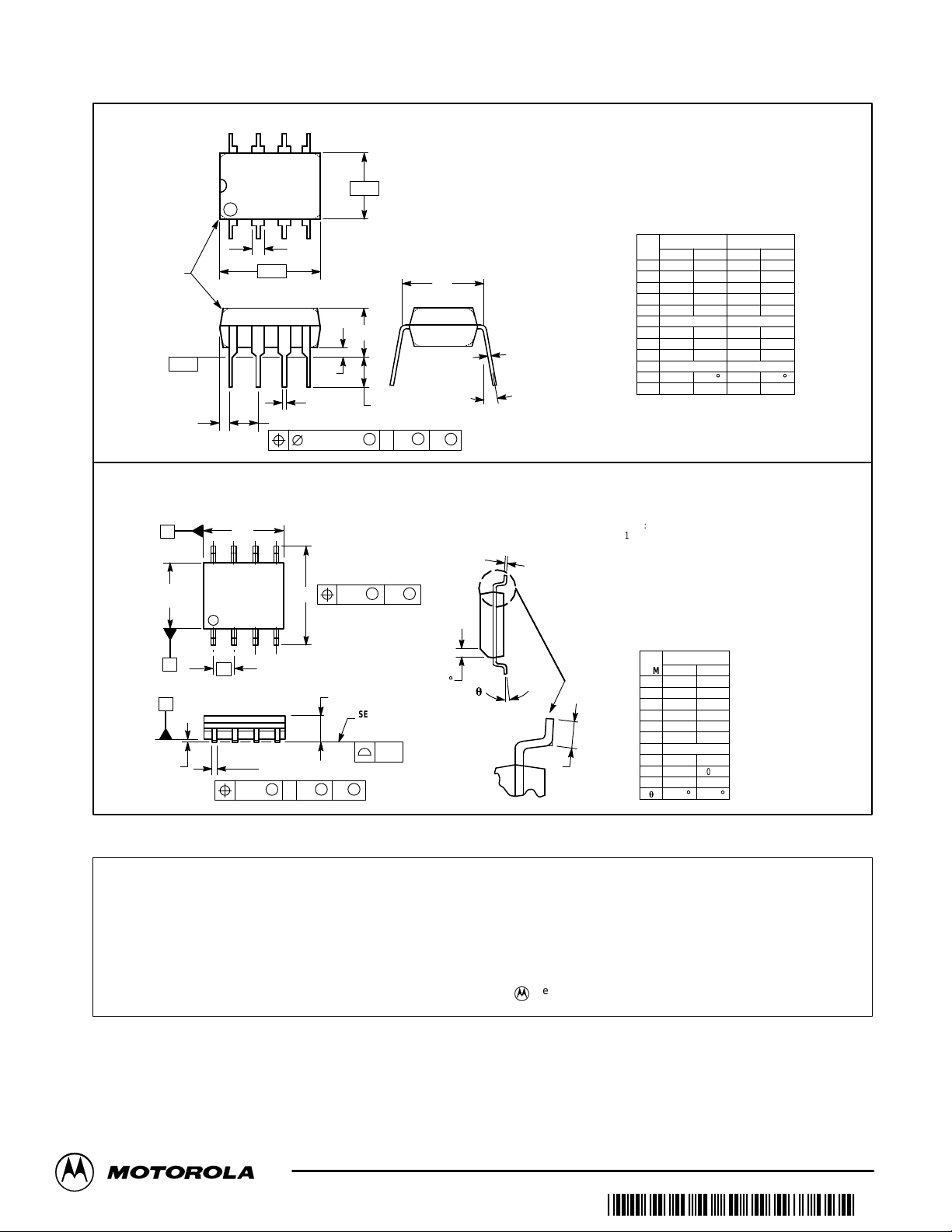
OUTLINE DIMENSIONS
P SUFFIX
PLASTIC PACKAGE
CASE 626–05
ISSUE K
L
J
M
M
A
M
D SUFFIX
PLASTIC PACKAGE
CASE 751–05
(SO–8)
ISSUE R
M
h
X 45
_
q
C
L
NOTES:
1. DIMENSION L TO CENTER OF LEAD WHEN
FORMED PARALLEL.
2. PACKAGE CONTOUR OPTIONAL (ROUND OR
SQUARE CORNERS).
3. DIMENSIONING AND TOLERANCING PER ANSI
Y14.5M, 1982.
DIM MIN MAX MIN MAX
A 9.40 10.16 0.370 0.400
B 6.10 6.60 0.240 0.260
C 3.94 4.45 0.155 0.175
D 0.38 0.51 0.015 0.020
F 1.02 1.78 0.040 0.070
G 2.54 BSC 0.100 BSC
H 0.76 1.27 0.030 0.050
J 0.20 0.30 0.008 0.012
K 2.92 3.43 0.115 0.135
L 7.62 BSC 0.300 BSC
M ––– 10 ––– 10
N 0.76 1.01 0.030 0.040
NOTES:
1. DIMENSIONING AND TOLERANCING PER ASME
Y14.5M, 1994.
2. DIMENSIONS ARE IN MILLIMETERS.
3. DIMENSION D AND E DO NOT INCLUDE MOLD
PROTRUSION.
4. MAXIMUM MOLD PROTRUSION 0.15 PER SIDE.
5. DIMENSION B DOES NOT INCLUDE MOLD
PROTRUSION. ALLOWABLE DAMBAR
PROTRUSION SHALL BE 0.127 TOTAL IN EXCESS
OF THE B DIMENSION AT MAXIMUM MATERIAL
CONDITION.
MILLIMETERS
DIM MIN MAX
A 1.35 1.75
A1 0.10 0.25
B 0.35 0.49
C 0.18 0.25
D 4.80 5.00
E
3.80 4.00
1.27 BSCe
H 5.80 6.20
h
0.25 0.50
L 0.40 1.25
0 7
q
INCHESMILLIMETERS
__
__
Motorola reserves the right to make changes without further notice to any products herein. Motorola makes no warranty , representation or guarantee regarding
the suitability of its products for any particular purpose, nor does Motorola assume any liability arising out of the application or use of any product or circuit, and
specifically disclaims any and all liability, including without limitation consequential or incidental damages. “T ypical” parameters which may be provided in Motorola
data sheets and/or specifications can and do vary in different applications and actual performance may vary over time. All operating parameters, including “Typicals”
must be validated for each customer application by customer’s technical experts. Motorola does not convey any license under its patent rights nor the rights of
others. Motorola products are not designed, intended, or authorized for use as components in systems intended for surgical implant into the body, or other
applications intended to support or sustain life, or for any other application in which the failure of the Motorola product could create a situation where personal injury
or death may occur. Should Buyer purchase or use Motorola products for any such unintended or unauthorized application, Buyer shall indemnify and hold Motorola
and its officers, employees, subsidiaries, affiliates, and distributors harmless against all claims, costs, damages, and expenses, and reasonable attorney fees
arising out of, directly or indirectly, any claim of personal injury or death associated with such unintended or unauthorized use, even if such claim alleges that
Motorola was negligent regarding the design or manufacture of the part. Motorola and are registered trademarks of Motorola, Inc. Motorola, Inc. is an Equal
Opportunity/Affirmative Action Employer.
How to reach us:
USA/EUROPE /Locations Not Listed: Motorola Literature Distribution; JAP AN: Nippon Motorola Ltd.; Tatsumi–SPD–JLDC, 6F Seibu–Butsuryu–Center,
P.O. Box 20912; Phoenix, Arizona 85036. 1–800–441–2447 or 602–303–5454 3–14–2 Tatsumi Koto–Ku, Tokyo 135, Japan. 03–81–3521–8315
MFAX: RMF AX0@email.sps.mot.com – TOUCHT ONE 602–244–6609 ASIA/PACIFIC: Motorola Semiconductors H.K. Ltd.; 8B Tai Ping Industrial Park,
INTERNET: http://Design–NET.com 51 Ting Kok Road, Tai Po, N.T., Hong Kong. 852–26629298
12
◊
MOTOROLA ANALOG IC DEVICE DATA
MC33077/D
*MC33077/D*
 Loading...