

Page 1
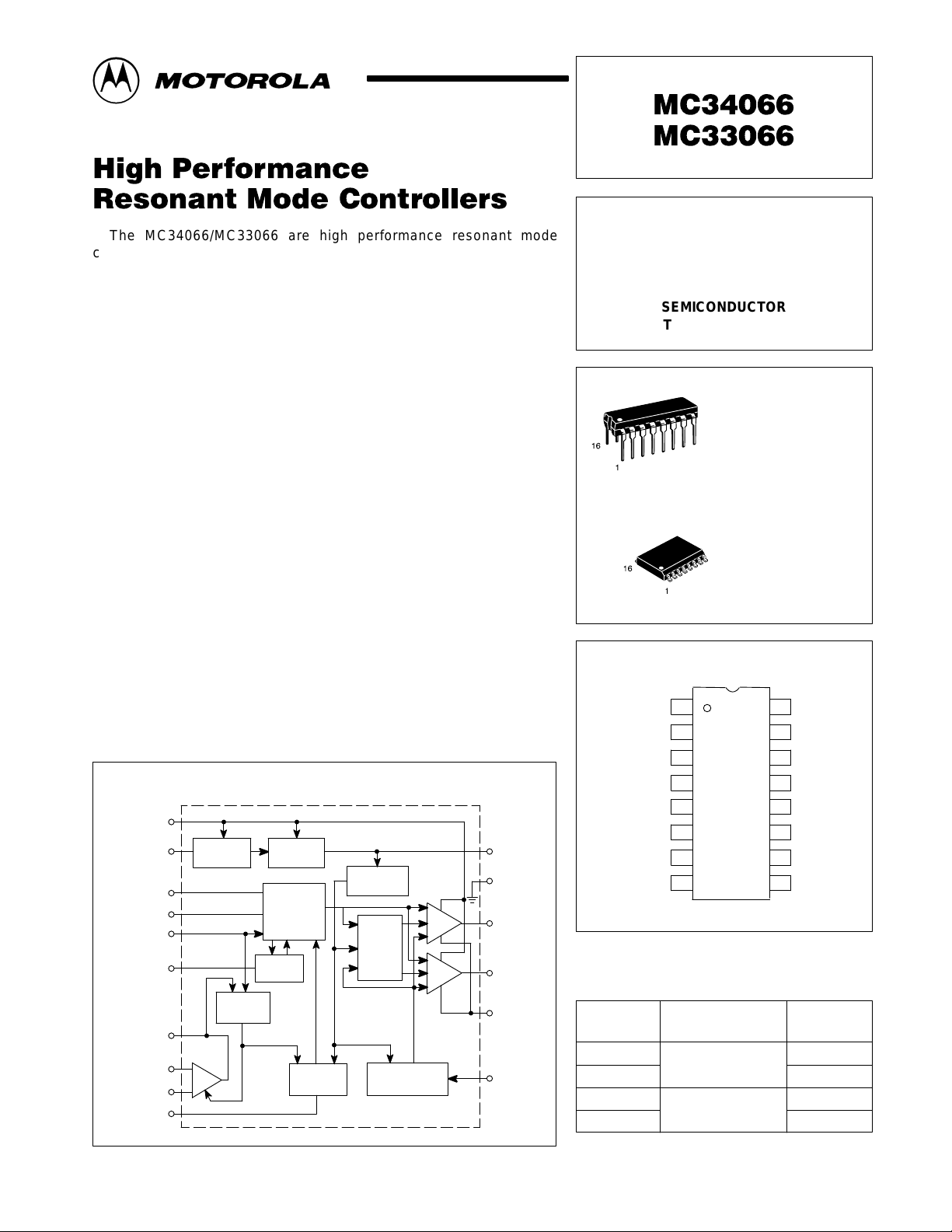
The MC34066/MC33066 are high performance resonant mode
controllers designed for off–line and dc–to–dc converter applications that
utilize frequency modulated constant on–time or constant off–time control.
These integrated circuits feature a variable frequency oscillator with
programmable deadtime, precision retriggerable one–shot timer,
temperature compensated reference, high gain wide–bandwidth error
amplifier with a precision output clamp, steering flip–flop, and dual high
current totem pole outputs ideally suited for driving power MOSFETs.
Also included are protective features consisting of a high speed fault
comparator and latch, programmable soft–start circuitry, input undervoltage
lockout with selectable thresholds, and reference undervoltage lockout.
These devices are available in dual–in–line and surface mount packages.
• V ariable Frequency Oscillator with a Control Range Exceeding 1000:1
• Programmable Oscillator Deadtime Allows Constant Off–Time Operation
• Precision Retriggerable One–Shot Timer
• Internally Trimmed Bandgap Reference
• 5.0 MHz Error Amplifier with Precision Output Clamp
• Dual High Current Totem Pole Outputs
• Selectable Undervoltage Lockout Thresholds with Hysteresis
• Enable Input
• Programmable Soft–Start Circuitry
• Low Startup Current for Off–Line Operation
Order this document by MC34066/D
HIGH PERFORMANCE
RESONANT MODE
CONTROLLERS
SEMICONDUCTOR
TECHNICAL DATA
P SUFFIX
PLASTIC PACKAGE
CASE 648
DW SUFFIX
PLASTIC PACKAGE
CASE 751G
(SO–16L)
PIN CONNECTIONS
V
CC
Enable/
UVLO Adjust
Osc
Deadtime
Osc RC
Osc Control
Current
One–Shot RC
Error Amp
Out
Error Amp +
Error Amp –
C
Soft–Start
15
9
1
2
3
16
6
8
7
11
VCC UVLO
Error Amp
Error
Amplifier
Simplified Block Diagram
Reference
Regulator
V
UVLO
Variable
Frequency
Oscillator
One–Shot
Clamp
Soft–Start
ref
Steering
Flip–Flop
Fault–Detector/
Latch
Osc Deadtime
Osc RC
Osc Control
Error Amp Out
V
ref
5
Gnd
4
A
out
B
out
Drive
Output A
14
Drive
Output B
12
Drive Gnd
13
Fault Input
10
Error Amp
Inverting Input
Error Amp
Noninverting Input
Device
MC34066DW
MC34066P
MC33066DW
MC33066P
1
2
3
Current
4
Gnd
5
V
ref
6
7
89
(Top View)
ORDERING INFORMATION
Operating
Temperature Range
TA = 0° to +70°C
TA = –40° to +85°C
16
One–Shot RC
15
V
CC
14
Drive Output A
13
Drive Gnd
12
Drive Output B
11
C
Soft–Start
10
Fault Input
Enable/UVLO
Adjust
Package
SO–16L
Plastic DIP
SO–16L
Plastic DIP
MOTOROLA ANALOG IC DEVICE DATA
Motorola, Inc. 1996 Rev 1
1
Page 2
MC34066 MC33066
MAXIMUM RATINGS
Rating Symbol Value Unit
Power Input Supply Voltage V
Drive Output Current, Source or Sink (Note 1)
Continuous
Pulsed (0.5 µs, 25% Duty Cycle)
Error Amplifier, Fault, One–Shot, Oscillator, and
Soft–Start Inputs
UVLO Adjust Input V
Soft–Start Discharge Current I
Power Dissipation and Thermal Characteristics
DW Suffix Package, Case 751G
Maximum Power Dissipation @ TA = 25°C
Thermal Resistance, Junction–to–Air
P Suffix Package, Case 648
Maximum Power Dissipation @ TA = 25°C
Thermal Resistance, Junction–to–Air
Operating Junction Temperature T
Operating Ambient Temperature
MC34066
MC33066
Storage Temperature Range T
CC
I
O
V
in
in(UVLO)
dchg
P
D
R
θJA
P
D
R
θJA
J
T
A
stg
20 V
0.3
1.5
–1.0 to +6.0 V
–1.0 to V
CC
20 mA
862
145
1.25
100
mW
°C/W
W
°C/W
+150 °C
°C
0 to +70
–40 to +85
–65 to +150 °C
A
V
ELECTRICAL CHARACTERISTICS (V
= 12 V [Note 2], R
CC
= 95.3 k, RDT = 0 Ω, R
OSC
= 5.62 k, C
VFO
= 300 pF, RT = 14.3 k,
OSC
CT = 300 pF, CL = 1.0 nF, for typical values TA = 25°C, for min/max values TA is the operating ambient temperature range that applies
[Note 3], unless otherwise noted.)
Characteristics
Symbol Min Typ Max Unit
REFERENCE SECTION
Reference Output Voltage (IO = 0 mA, TA = 25°C) V
Line Regulation (VCC = 10 V to 18 V) Reg
Load Regulation (IO = 0 mA to 10 mA) Reg
Total Output Variation over Line, Load, and Temperature V
Output Short Circuit Current I
Reference Undervoltage Lockout Threshold V
ref
line
load
ref
O
th
5.0 5.1 5.2 V
– 1.0 20 mV
– 1.0 20 mV
4.9 – 5.3 mV
25 100 190 mA
3.8 4.3 4.8 V
ERROR AMPLIFIER
Input Offset Voltage (VCM = 1.5 V) V
Input Bias Current (VCM = 1.5 V) I
Input Offset Current (VCM = 1.5 V) I
Open Loop Voltage Gain (VCM = 1.5 V, VO = 2.0 V) A
IO
IB
IO
VOL
– 1.0 10 mV
– 0.2 1.0 µA
– 0 0.5 µA
70 100 – dB
Gain Bandwidth Product (f = 100 kHz) GBW 2.5 4.2 – MHz
Input Common Mode Rejection Ratio (VCM = 1.5 V to 5.0 V) CMRR 70 95 – dB
Power Supply Rejection Ratio (VCC = 10 V to 18 V, f = 120 Hz) PSRR 80 100 – dB
Output Voltage Swing
High State with Respect to Pin 3 (I
Low State with Respect to Ground (I
NOTES: 1. Maximum package power dissipation limits must be observed.
2.Adjust VCC above the Startup threshold before setting to 12 V.
3.Low duty cycle pulse techniques are used during test to maintain junction temperature as close to ambient as possible.
T
=0°C for MC34066 T
low
–40°C for MC33066 T
= 2.0 mA)
Source
= 1.0 mA)
Sink
= +70°C for MC34066
high
= +85°C for MC33066
high
V
OH
V
OL
2.3
–
2.7
0.4
3.1
0.6
V
2
MOTOROLA ANALOG IC DEVICE DATA
Page 3
MC34066 MC33066
ELECTRICAL CHARACTERISTICS (continued) (V
= 12 V [Note 2], R
CC
= 95.3 k, RDT = 0 Ω, R
OSC
VFO
= 5.62 k, C
OSC
= 300 pF,
RT = 14.3 k, CT = 300 pF, CL = 1.0 nF, for typical values TA = 25°C, for min/max values TA is the operating ambient temperature range that
applies [Note 3], unless otherwise noted.)
Characteristics
Symbol Min Typ Max Unit
OSCILLAT OR
Frequency (Error Amp Output Low)
TA = 25°C
Total Variation (VCC = 10 V to 18 V, TA = T
Frequency (Error Amp Output High)
TA = 25°C
Total Variation (VCC = 10 V to 18 V, TA = T
Oscillator Control Input Voltage, Pin 3 (I
Sink
Output Deadtime (Error Amp Output High)
RDT = 0 Ω
RDT = 1.0 k
Low
Low
to T
to T
High
High
)
)
= 0.5 mA, TA = 25°C) V
f
OSC(low)
f
OSC(high)
in
DT
90
85
900
850
100
–
110
115
1000–1100
1150
1.3 1.4 1.5 V
–
600
70
700
100
800
kHz
kHz
ns
ONE–SHOT
Drive Output On–Time (RDT = 1.0 k)
TA = 25°C
Total Variation (VCC = 10 V to 18 V, TA = T
Low
to T
High
)
t
OS
1.43
1.4
1.5
1.57
µs
–
1.6
DRIVE OUTPUTS
Output Voltage
Low State (I
Low State (I
High State (I
High State (I
Output Voltage with UVLO Activated (VCC = 6.0 V, I
= 20 mA)
Sink
= 200 mA)
Sink
Source
Source
= 20 mA)
= 200 mA)
= 1.0 mA) V
Sink
V
OL(UVLO)
Output Voltage Rise T ime (CL = 1.0 nF) t
Output Voltage Fall T ime (CL = 1.0 nF) t
V
OL
OH
–
–
9.5
9.0
0.8
1.5
10.3
9.8
1.2
2.0
–
–
– 0.8 1.2 V
r
f
– 20 50 ns
– 20 50 ns
V
FAULT COMPARATOR
Input Threshold V
Input Bias Current (V
Propagation Delay to Drive Outputs (100 mV Overdrive) t
= 0 V) I
Pin 10
PLH(In/Out)
th
IB
0.95 1.0 1.05 V
– –2.0 –10 µA
– 60 100 ns
SOFT–START
Capacitor Charge Current (V
Capacitor Discharge Current (V
= 2.5 V) I
Pin 11
= 2.5 V) I
Pin 11
chg
Idchg
4.5 8.1 14 µA
1.0 8.0 – mA
UNDERVOLTAGE LOCKOUT
Startup Threshold, VCC Increasing
Enable/UVLO Adjust Pin Open
Enable/UVLO Adjust Pin Connected to V
CC
Minimum Operating Voltage after Turn–On
Enable/UVLO Adjust Pin Open
Enable/UVLO Adjust Pin Connected to V
CC
Enable/UVLO Adjust Shutdown Threshold Voltage V
Enable/UVLO Adjust Input Current (Pin 9 = 0V) I
V
th(UVLO)
V
CC(min)
th(Enable)
in(Enable)
14.8
8.0
8.0
7.6
16
9.0
9.0
8.6
17.2
10
10
9.6
6.0 7.0 – V
– –0.2 –1.0 mA
V
V
TOTAL DEVICE
Power Supply Current (Enable/UVLO Adjust Pin Open)
Startup (VCC = 13.5 V)
Operating (f
NOTES: 2. Adjust VCC above the Startup threshold before setting to 12 V.
3.Low duty cycle pulse techniques are used during test to maintain junction temperature as close to ambient as possible.
T
low
= 100 kHz) (Note 2)
OSC
=0°C for MC34066 T
–40°C for MC33066 T
= +70°C for MC34066
high
= +85°C for MC33066
high
I
CC
0.45
–
21
0.6
30
–
mA
MOTOROLA ANALOG IC DEVICE DATA
3
Page 4
V
CC
Enable/
UVLO Adjust
Osc Deadtime
R
DT
R
OSC
C
T
Error Amp
Inverting Input
Noninverting Input
C
Soft–Start
Osc RC
C
OSC
One–Shot RC
R
T
Osc Control
Current
I
OSC
Output
Error Amp
Error Amp
R
15
9
1
2
16
3
VFO
6
7
8
11
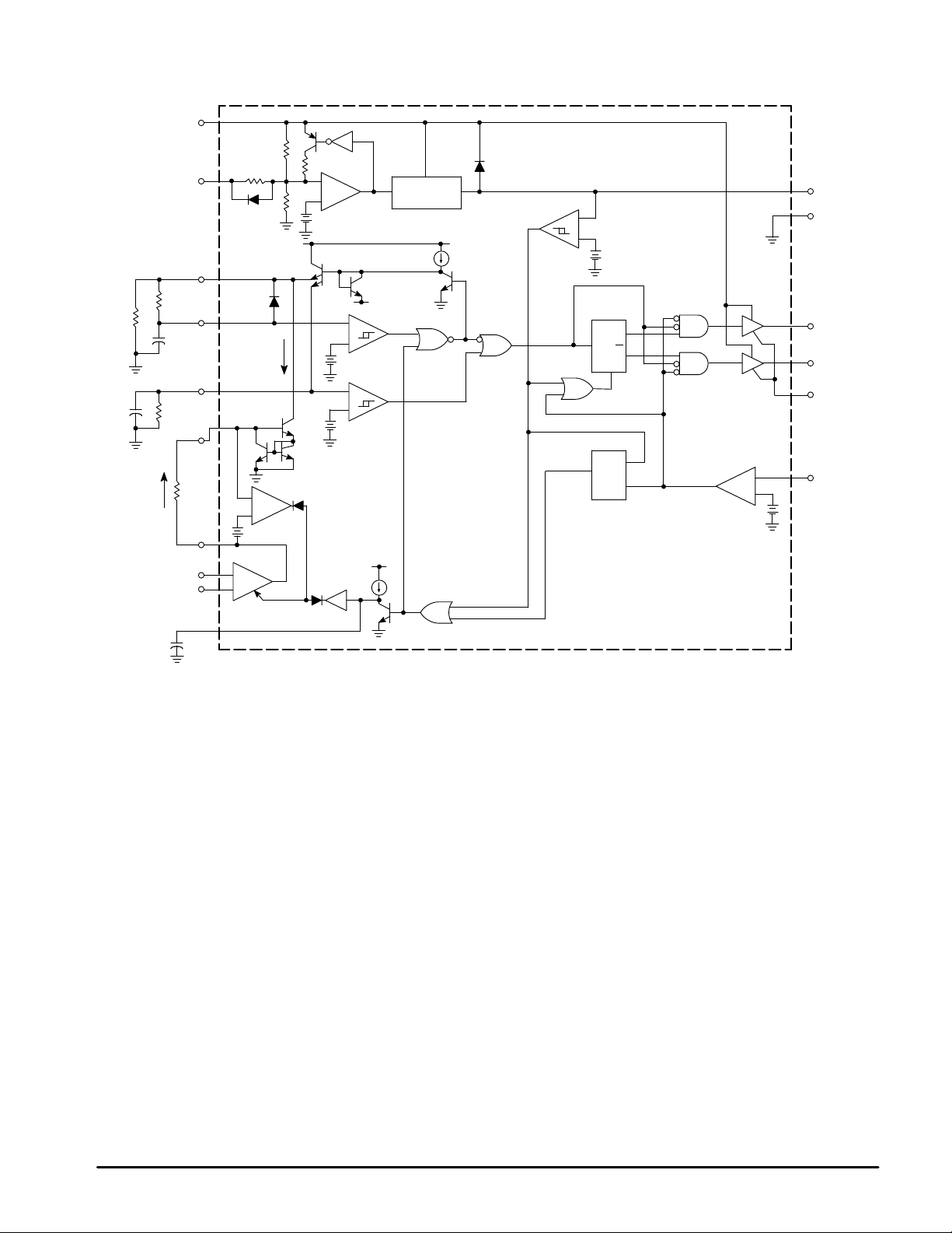
Figure 1. MC34066 Representative Block Diagram
50k
7k
I
OSC
+
–
2.5V EA Clamp
–
+
Error
Amplifier
7k
+
50k
–
8V
Q1
Current Mirror
Error Amp
Output Clamp
Soft–Start
Buffer
VCC UVLO
V
CC
Q2
Oscillator
–
+
4.9V/3.6V
One–Shot
–
+
4.9V/3.6V
µ
A
9
MC34066 MC33066
Reference
Regulator
5.1V
UVLO + Fault
5.1V
V
UVLO
UVLO
ref
–
+
t
on
4.2V/4V
Steering
Flip–Flop
Q
T
Q
R
R
Q
S
Fault
Latch
Drivers
Fault
Comparator
Fault
+
–
1.0V
5
4
14
12
13
10
V
ref
Gnd
Drive
Output A
Drive
Output B
Drive
Gnd
Fault
Input
OPERA TING DESCRIPTION
Introduction
As power supply designers have strived to increase power
conversion efficiency and reduce passive component size,
high frequency resonant mode power converters have
emerged as attractive alternatives to conventional
square–wave control. When compared to square–wave
converters, resonant mode control offers several benefits
including lower switching losses, higher efficiency , lower EMI
emission, and smaller size. This integrated circuit has been
developed to support new trends in power supply design.
The MC34066 Resonant Mode Controller is a high
performance bipolar IC dedicated to variable frequency
power control at frequencies exceeding 1.0 MHz. This
integrated circuit provides the features, performance and
flexibility for a wide variety of resonant mode power supply
applications.
The primary purpose of the control chip is to supply
precise pulses to the gates of external power MOSFETs at a
repetition rate regulated by a feedback control loop. The
MC34066 can be operated in any of three modes as follows:
1) fixed on–time, variable frequency; 2) fixed off–time,
variable frequency; and 3) combinations of 1 and 2 that
change from fixed on–time to fixed off–time as the frequency
increases. Additional features of the IC ensure that system
startup and fault conditions are administered in a safe,
controlled manner.
A simplified block diagram of the IC is shown on the first
page of this data sheet, which identifies the main functional
blocks and the block–to–block interconnects. Figure 1 is a
detailed functional diagram which accurately represents the
internal circuitry. The various functions can be divided into
two sections. The first section includes the primary control
path which produces precise output pulses at the desired
frequency Oscillator, a One–Shot, a pulse Steering Flip–Flop,
a pair of power MOSFET Drivers, and a wide bandwidth Error
Amplifier. The second section provides several peripheral
support functions including a voltage reference, undervoltage
lockout, Soft–Start circuit, and a fault detector.
Primary Control Path
The output pulse width and repetition rate are regulated
through the interaction of the variable frequency Oscillator,
One–Shot timer and Error Amplifier. The Oscillator triggers
the One–Shot which generates a pulse that is alternately
steered to a pair of totem–pole output drivers by a toggle
Flip–Flop. The Error Amplifier monitors the output of the
regulator and modulates the frequency of the Oscillator.
High–speed Schottky logic is used throughout the primary
control channel to minimize delays and enhance high
frequency characteristics.
4
MOTOROLA ANALOG IC DEVICE DATA
Page 5

MC34066 MC33066
Oscillator
The characteristics of the variable frequency Oscillator are
crucial for precise controller performance at high operating
frequencies. In addition to triggering the One–Shot timer and
initiating the output pulse, the Oscillator also determines the
initial voltage for the One–Shot capacitor and defines the
minimum deadtime between output pulses. The Oscillator is
designed to operate at frequencies exceeding 1.0 MHz. The
Error Amplifier can control the oscillator frequency over a
1000:1 frequency range, and both the minimum and
maximum frequencies are easily and accurately
programmed by the proper selection of external components.
The Oscillator also includes an adjustable deadtime feature
for applications requiring additional time between output
pulses.
The functional diagram of the Oscillator and One–Shot
timer is shown in Figure 2. The oscillator capacitor C
initially charged by transistor Q1 through the optional
deadtime resistor RDT. When C
exceeds the 4.9 V upper
OSC
threshold of the oscillator comparator, the base of Q1 is
pulled low allowing C
to discharge through the external
OSC
resistors and the internal Current Mirror. When the voltage on
C
falls below the comparator’s 3.6 V lower threshold, Q1
OSC
turns on and again charges C
OSC
.
Figure 2. Oscillator and One–Shot Timer
V
CC
OSC
is
2.5ROSC
t
dchg(min)
= (RDT + R
OSC)COSC
In
2.5ROSC
RVFO
RVFO
The minimum oscillator frequency will result when the I
current is zero, and C
resistors R
and RDT. This occurs when the Error Amplifier
OSC
is discharged through the external
OSC
+ 5.1
(1)
+ 3.6
OSC
output voltage is less than the two diode drops required to
bias the input of the Current Mirror. The maximum oscillator
discharge time is given by Equation 2.
t
dchg(max)
= (RDT + R
OSC
) C
OSC
5.1
In (2)
3.6
The outputs of the control IC are off whenever the oscillator
capacitor C
is being charged by transistor Q1. The
OSC
minimum time between output pulses (deadtime) can be
programmed by controlling the charge time of C
RDT reduces the current delivered by Q1 to C
increasing the charge time and output deadtime. V arying R
OSC
. Resistor
, thus
OSC
DT
from 0 Ω to 1000 Ω will increase the output deadtime from
80 ns to 680 ns with C
equal to 300 pF. The general
OSC
expression for the oscillator charge time is give by
Equation 3.
t
chg(max)
= RDT C
OSC
In
5.1–3.6
5.1–4.9
+ 80 ns
(3)
Osc Deadtime
1
R
DT
R
OSC
C
T
If RDT is 0 Ω, C
Osc RC
C
OSC
One–Shot RC
R
T
Osc Control
Current
I
OSC
Error Amp
Output
R
2
I
16
3
VFO
6
OSC
50 ns. The high slew rate of C
Q1
Q2
5.1V
Oscillator
–
OSC
Current Mirror
+
4.9V/3.6V
One–Shot
–
+
4.9V/3.6V
UVLO + Fault
charges from 3.6 V to 5.1 V in less than
and the propagation delay
OSC
of the comparator make it difficult to control the peak voltage.
This accuracy issue is overcome by clamping the base of Q1
through diode Q2 to a voltage reference. The peak voltage of
the oscillator waveform is thereby precisely set at 5.1 V.
The frequency of the Oscillator is modulated by varying the
current I
flowing through R
OSC
into the Osc Control
VFO
Current pin. The control current drives a unity gain Current
Mirror which pulls an identical current from the C
capacitor. As I
increases, C
OSC
discharges faster thus
OSC
OSC
decreasing the Oscillator period and increasing the
frequency. The maximum frequency occurs when the Error
Amplifier output is at the upper clamp level, nominally 2.5 V
above the voltage at the Osc Control Current pin. The
minimum discharge time for C
, which corresponds to the
OSC
maximum oscillator frequency , is given by Equation 1.
The minimum and maximum oscillator frequencies are
programmed by the proper selection of resistor R
R
. After selecting RDT for the desired deadtime, the
VFO
minimum frequency is programmed by R
OSC
OSC
using
and
Equations 2 and 3 in Equation 4:
1
= t
f
OSC(min)
dchg(max)
The maximum oscillator frequency is set by resistor R
+ t
chg
(4)
VFO
in a similar fashion using Equations 1 and 3 in Equation 5:
1
f
OSC(max)
= t
dchg(min)
+ t
chg
(5)
The value chosen for resistor RDT will affect the peak
voltage of the oscillator waveform. As RDT is increased from
zero, the time required to charge C
becomes large with
OSC
respect to the propagation delay through the oscillator
comparator. Consequently, the overshoot of the upper
threshold is reduced and the peak voltage on the oscillator
waveform drops from 5.1 V to 4.9 V. The best frequency
accuracy is achieved when RDT is zero ohms.
One–Shot Timer
The One–Shot capacitor CT is charged concurrently with
the oscillator capacitor by transistor Q1, as shown in Figure 2.
The One–Shot period begins when the oscillator comparator
turns off Q1, allowing CT to discharge. The period ends when
resistor RT discharges CT to the threshold of the One–Shot
comparator. Discharging CT from an initial voltage of 5.1 V to
a threshold voltage of 3.6 V results in the One–Shot period
given by Equation 6.
tOS = RT CT In (6)
5.1
= 0.348 RT C
3.6
T
MOTOROLA ANALOG IC DEVICE DATA
5
Page 6

5.1 V
C
OSC
MC34066 MC33066
Figure 3. Timing Waveforms
RDT = 0
t
> t
dchg
One–Shot
t
dchg
< t
One–Shot
5.1 V
4.9 V
3.6 V
5.1 V
3.6 V
A
OUT
B
OUT
t
dchg
C
T
t
OS
t
on
t
on
t
t
off
on
t
dchg
RDT = 1.0 k
t
t
dchg
> t
One–Shot
dchg
< t
One–Shot
C
OSC
3.6 V
5.1 V
3.6 V
A
OUT
B
OUT
t
t
chg
C
T
t
on
t
t
OS
on
t
dchg
t
off
t
on
chg
t
dchg
6
MOTOROLA ANALOG IC DEVICE DATA
Page 7

MC34066 MC33066
Errors in the threshold voltage and propagation delays
through the output drivers will affect the One–Shot period. To
guarantee accuracy, the output pulse of the control ship is
trimmed to within 5% of 1.5 µs with nominal values of R
and CT.
The outputs of the Oscillator and One–Shot comparators
are OR’d together to produce the pulse ton, which drives the
Flip–Flop and output drivers. The output pulse ton is initiated
by the Oscillator, but either the oscillator comparator or the
One–Shot comparator can terminate the pulse. When the
oscillator discharge time exceeds the one–shot period, the
complete one–shot period is delivered to the output section. If
the oscillator discharge time is less than the one–shot period,
then the oscillator comparator terminates the pulse
prematurely and retriggers the One–Shot. The waveforms on
the left side of Figure 3 correspond to nonretriggered
operation with constant on–time and variable off–times. The
right side of Figure 3 represents retriggered operation with
variable on–time and constant off–time.
Error Amplifier
A fully accessible high performance Error Amplifier is
provided for feedback control of the power supply system.
The Error Amplifier is internally compensated and features dc
open loop gain greater than 70 dB, input offset voltage less
than 10 mV and guaranteed minimum gain–bandwidth
product of 2.5 MHz. The input common mode range extends
from 1.5 V to 5.1 V, which includes the reference voltage. For
common mode voltages below 1.5 V, the Error Amplifier
output is forced low providing minimum oscillator frequency.
The Oscillator Control Current pin is biased by the Error
Amplifier output voltage through R
as illustrated in Figure
VFO
4. The output swing of the Error Amplifier is restricted by a
clamp circuit to limit the maximum oscillator frequency. The
clamp circuit limits the voltage across R
thus limiting I
to 2.5 V/R
OSC
. Oscillator accuracy is
VFO
to 2.5 V,
VFO
improved by trimming the clamp voltage to obtain the
f
OSC(high)
specification of 1.0 MHz with nominal value
external components.
Figure 4. Error Amplifier and Clamp
Osc Control
Current
3
OSC
Output
Error Amp
Error Amp
R
VFO
6
7
8
+
–
2.5V
+
–
Error
Amplifier
Error Amp
Output Clamp
EA Clamp
I
Error Amp
Noninverting Input
Inverting Input
Output Section
The pulse, ton, generated by the Oscillator and One–Shot
timer is gated to dual totem pole output drives by the Steering
Flip–Flop shown in Figure 5. Positive transitions of ton toggle
T
the Flip–Flop, which causes the pulses to alternate between
Output A and Output B. The flip–flop is reset by the
undervoltage lockout circuit during startup to guarantee that
the first pulse appears at Output A.
The totem–pole output drives are ideally suited for driving
power MOSFETs and are capable of sourcing and sinking
1.5 A. Rise and fall times are typically 20 ns when driving a
1.0 nF load. High source/sink capability in a totem–pole
driver normally increases the risk of high cross conduction
current during output transitions. The MC34066 utilizes a
unique design that virtually eliminates cross conduction, thus
controlling the chip power dissipation at high frequencies. A
separate ground terminal is provided for the output drivers to
isolate the sensitive analog circuitry from large
transient currents.
Figure 5. Steering Flip–Flop and Output Drivers
V
CC
Drivers
UVLO
t
on
Steering
Flip–Flop
Q
T
Q
R
Fault
PERIPHERAL SUPPORT FUNCTIONS
The MC34066 Resonant Controller provides a number of
support and protection functions including a precision voltage
reference, undervoltage lockout comparators, soft–start
circuitry, and a fault detector . These peripheral circuits ensure
that the power supply can be turned on and off in a safe,
controlled manner and that the system will be quickly
disabled when a fault condition occurs.
Undervoltage Lockout and V oltage Reference
Separate undervoltage lockout comparators sense the
input VCC voltage and the regulated reference voltage as
illustrated in Figure 6. When VCC increases to the upper
threshold voltage, the VCC UVLO comparator enables the
Reference Regulator. After the V
Regulator rises to 4.2 V , the V
output of the Reference
ref
UVLO comparator switches
ref
the UVLO signal to a logic zero state enabling the primary
control path. Reducing VCC to the lower threshold voltage
causes the VCC UVLO comparator to disable the Reference
Regulator. The V
UVLO comparator then switches the
ref
UVLO output to a logic one state disabling the controller.
14
12
13
Drive
Output A
Drive
Output B
Drive
Gnd
MOTOROLA ANALOG IC DEVICE DATA
7
Page 8

V
CC
Enable/
UVLO Adjust
15
MC34066 MC33066
Figure 6. Undervoltage Lockout and Reference
50k
7k
9
50k
7k
+
–
VCC UVLO
8.0V
Reference
Regulator
5.1V V
UVLO
ref
UVLO
–
+
4.2V/4.0V
V
ref
5
Gnd
4
The Enable/UVLO Adjust terminal allows the power supply
designer to select the VCC UVLO threshold voltages. When
this pin is open, the comparator switches the controller on at
16 V and off at 9.0 V. If this pin is connected to the V
CC
terminal, the upper and lower thresholds are reduced to 9.0 V
and 8.6 V, respectively. Forcing the Enable/UVLO Adjust pin
low will pull the VCC UVLO comparator input low (through an
internal diode) turning off the controller.
The Reference Regulator provides a precise 5.1 V
reference to internal circuitry and can deliver up to 10 mA to
external loads. The reference is trimmed to better than 2%
initial accuracy and includes active short circuit protection.
Fault Detector
The high–speed Fault Comparator and Latch illustrated in
Figure 7 can protect a power supply from destruction under
fault conditions. The Fault Input pin connects to the input of
the Fault Comparator. If this input exceeds the 1.0 V
threshold of the comparator, the Fault Latch is set and two
logic signals simultaneously disable the primary control path.
The signal labeled Fault at the output of the Fault Comparator
is connected directly to the output drivers. This direct path
reduces the propagation delay from the Fault Input to the A
and B outputs to typically 70 ns. The Fault Latch output is
OR’d with UVLO output from the V
UVLO comparator to
ref
produce the logic output labeled UVLO + Fault. This signal
disables the Oscillator and One–Shot by forcing both the
C
and CT capacitors to be continually charged.
OSC
Figure 7. Fault Detector and Soft–Start
UVLOUVLO + Fault
EA Clamp
9µA
Soft–Start
Buffer
QRS
Fault
Latch
Fault
Fault
Comparator
Fault
Input
+
10
–
1V
C
Soft–
Start
11
The Fault Latch is reset during startup by a logic one at the
UVLO output of the V
UVLO comparator. The latch can also
ref
be reset after startup by pulling the Enable/UVLO Adjust pin
momentarily low to disable the Reference Regulator.
Soft–Start Circuit
The Soft–Start circuit shown in Figure 7 forces the variable
frequency Oscillator to start at the minimum frequency and
ramp upward until regulated by the feedback control loop.
The external capacitor at the C
Soft–Start
terminal is initially
discharged by the UVLO + Fault signal. The low voltage on
the capacitor pass through the Soft–Start Buffer to hold the
Error Amplifier output low. After UVLO + Fault switches to a
logic zero, the soft–start capacitor is charged by a 9.0 µA
current source. The buffer allows the Error Amplifier output to
follow the soft–start capacitor until it is regulated by the Error
Amplifier inputs (or reaches the 2.5 V clamp). The soft–start
function is generally applicable to controllers operating below
resonance and can be disabled by simply opening the
C
Soft–Start
terminal.
APPLICATIONS
The MC34066 can be used for the control of series,
parallel or higher order half/full bridge resonant converters.
The IC is designed to provide control in discontinuous
conduction mode (DCM) or continuous conduction mode
(CCM) or a combination of the two. For example, in a parallel
resonant converter (PRC) operating in the DCM, the IC is
programmed to operate in fixed on–time, variable frequency
mode of operation. For a PRC operating in the CCM, the IC
can be programmed to operate in the variable frequency
mode with a fixed off–time.
When operating with a wide input voltage range, such as a
universal input power supply , a PRC can operate in the DCM
for high input voltage and in the CCM for low input voltage. In
this particular case, on–time is programmed corresponding to
DCM. The deadtime of the chip is programmed to provide the
desired off–time in the CCM. The frequency range is chosen
to cover the complete frequency range from the DCM to the
CCM. When programmed as such, the controller will operate
in the fixed on–time, variable frequency mode at low
frequencies. At the frequency which causes the Oscillator to
retrigger the One–Shot, the control law changes to variable
frequency with fixed off–time. At higher frequencies the
supply will operate in the CCM with this control law.
Although the IC is designed and optimized for double
ended push–pull type converters, it can also be used for
single ended applications, such as forward and flyback
resonant converters.
8
MOTOROLA ANALOG IC DEVICE DATA
Page 9

MC34066 MC33066
OUTLINE DIMENSIONS
P SUFFIX
PLASTIC PACKAGE
CASE 648–08
ISSUE R
–A–
916
B
18
F
C
S
SEATING
–T–
PLANE
H
G
D
16 PL
0.25 (0.010) T
K
M
M
A
PLASTIC PACKAGE
CASE 751G–02
–A–
16 9
–B– P8X
M
J
81
D16X
0.010 (0.25) B
M
S
A
T
0.010 (0.25)
S
F
C
–T–
G14X
K
SEATING
PLANE
M
J
DW SUFFIX
(SO–16L)
ISSUE A
M
B
R
L
X 45
NOTES:
1. DIMENSIONING AND TOLERANCING PER ANSI
Y14.5M, 1982.
2. CONTROLLING DIMENSION: INCH.
3. DIMENSION L TO CENTER OF LEADS WHEN
FORMED PARALLEL.
4. DIMENSION B DOES NOT INCLUDE MOLD FLASH.
5. ROUNDED CORNERS OPTIONAL.
DIM MIN MAX MIN MAX
A 0.740 0.770 18.80 19.55
B 0.250 0.270 6.35 6.85
C 0.145 0.175 3.69 4.44
D 0.015 0.021 0.39 0.53
F 0.040 0.70 1.02 1.77
G 0.100 BSC 2.54 BSC
M
NOTES:
_
H 0.050 BSC 1.27 BSC
J 0.008 0.015 0.21 0.38
K 0.110 0.130 2.80 3.30
L 0.295 0.305 7.50 7.74
M 0 10 0 10
S 0.020 0.040 0.51 1.01
1. DIMENSIONING AND TOLERANCING PER ANSI
Y14.5M, 1982.
2. CONTROLLING DIMENSION: MILLIMETER.
3. DIMENSIONS A AND B DO NOT INCLUDE MOLD
PROTRUSION.
4. MAXIMUM MOLD PROTRUSION 0.15 (0.006) PER
SIDE.
5. DIMENSION D DOES NOT INCLUDE DAMBAR
PROTRUSION. ALLOWABLE DAMBAR
PROTRUSION SHALL BE 0.13 (0.005) TOTAL IN
EXCESS OF D DIMENSION AT MAXIMUM
MATERIAL CONDITION.
DIM MIN MAX MIN MAX
A 10.15 10.45 0.400 0.411
B 7.40 7.60 0.292 0.299
C 2.35 2.65 0.093 0.104
D 0.35 0.49 0.014 0.019
F 0.50 0.90 0.020 0.035
G 1.27 BSC 0.050 BSC
J 0.25 0.32 0.010 0.012
K 0.10 0.25 0.004 0.009
M 0 7 0 7
____
P 10.05 10.55 0.395 0.415
R 0.25 0.75 0.010 0.029
MILLIMETERSINCHES
____
INCHESMILLIMETERS
MOTOROLA ANALOG IC DEVICE DATA
9
Page 10

MC34066 MC33066
NOTES
10
MOTOROLA ANALOG IC DEVICE DATA
Page 11

MC34066 MC33066
NOTES
MOTOROLA ANALOG IC DEVICE DATA
11
Page 12

MC34066 MC33066
Motorola reserves the right to make changes without further notice to any products herein. Motorola makes no warranty , representation or guarantee regarding
the suitability of its products for any particular purpose, nor does Motorola assume any liability arising out of the application or use of any product or circuit, and
specifically disclaims any and all liability, including without limitation consequential or incidental damages. “T ypical” parameters which may be provided in Motorola
data sheets and/or specifications can and do vary in different applications and actual performance may vary over time. All operating parameters, including “Typicals”
must be validated for each customer application by customer’s technical experts. Motorola does not convey any license under its patent rights nor the rights of
others. Motorola products are not designed, intended, or authorized for use as components in systems intended for surgical implant into the body, or other
applications intended to support or sustain life, or for any other application in which the failure of the Motorola product could create a situation where personal injury
or death may occur. Should Buyer purchase or use Motorola products for any such unintended or unauthorized application, Buyer shall indemnify and hold Motorola
and its officers, employees, subsidiaries, affiliates, and distributors harmless against all claims, costs, damages, and expenses, and reasonable attorney fees
arising out of, directly or indirectly, any claim of personal injury or death associated with such unintended or unauthorized use, even if such claim alleges that Motorola
was negligent regarding the design or manufacture of the part. Motorola and are registered trademarks of Motorola, Inc. Motorola, Inc. is an Equal
Opportunity/Affirmative Action Employer.
How to reach us:
USA/EUROPE/Locations Not Listed: Motorola Literature Distribution; JAPAN: Nippon Motorola Ltd.; Tatsumi–SPD–JLDC, 6F Seibu–Butsuryu–Center,
P.O. Box 20912; Phoenix, Arizona 85036. 1–800–441–2447 or 602–303–5454 3–14–2 T atsumi Koto–Ku, Tokyo 135, Japan. 03–81–3521–8315
MFAX: RMF AX0@email.sps.mot.com – TOUCHT ONE 602–244–6609 ASIA/PACIFIC: Motorola Semiconductors H.K. Ltd.; 8B Tai Ping Industrial Park,
INTERNET: http://Design–NET .com 51 Ting Kok Road, Tai Po, N.T., Hong Kong. 852–26629298
12
◊
MOTOROLA ANALOG IC DEVICE DATA
MC34066/D
*MC34066/D*
 Loading...