

Page 1
Order this document by MC33039/D
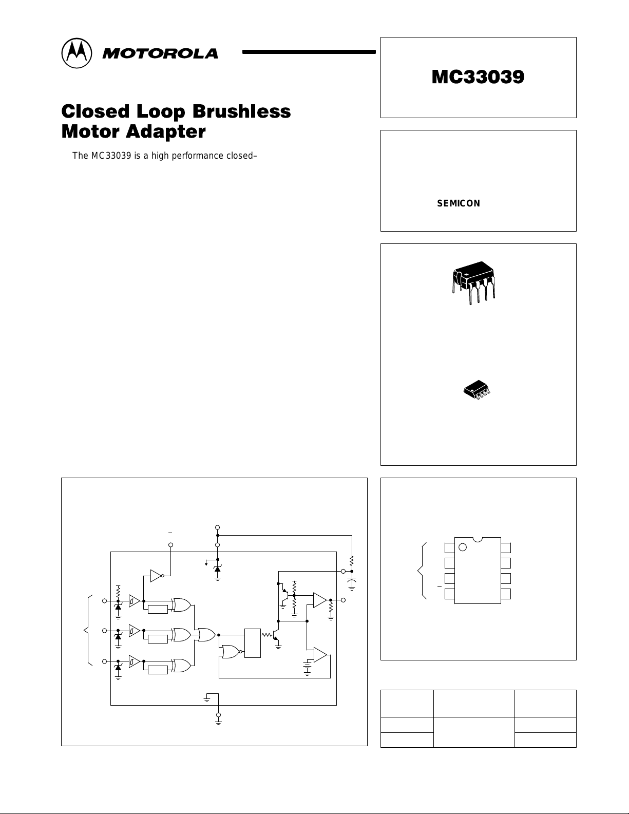
The MC33039 is a high performance closed–loop speed control adapter
specifically designed for use in brushless DC motor control systems.
Implementation will allow precise speed regulation without the need for a
magnetic or optical tachometer. This device contains three input buffers
each with hysteresis for noise immunity, three digital edge detectors, a
programmable monostable, and an internal shunt regulator. Also included is
an inverter output for use in systems that require conversion of sensor
phasing. Although this device is primarily intended for use with the MC33035
brushless motor controller, it can be used cost effectively in many other
closed–loop speed control applications.
• Digital Detection of Each Input Transition for Improved Low
Speed Motor Operation
• TTL Compatible Inputs With Hysteresis
• Operation Down to 5.5 V for Direct Powering from MC33035 Reference
• Internal Shunt Regulator Allows Operation from a Non–Regulated
Voltage Source
• Inverter Output for Easy Conversion between 60°/300° and 120°/240°
Sensor Phasing Conventions
CLOSED LOOP
BRUSHLESS MOTOR
ADAPTER
SEMICONDUCTOR
TECHNICAL DATA
8
1
P SUFFIX
PLASTIC PACKAGE
CASE 626
8
1
D SUFFIX
PLASTIC PACKAGE
CASE 751
(SO–8)
Representative Block Diagram
V
CC
φ
A
T o Rotor
Position
Sensors
4
+
20 k
3
φ
A
2
φ
B
1
φ
C
Delay
Delay
Delay
8
+
8.25 V
7
Gnd
MOTOROLA ANALOG IC DEVICE DATA
PIN CONNECTIONS
φ
1
R
T
6
+
R
+
2R
–
15 k
QS
R
+
–
+
0.3 V
C
T
5
f
out
Inputs
C
2
φ
B
φ
3
A
4
φ
A
(Top View)
V
8
CC
Gnd
7
RT/C
6
T
5
f
out
ORDERING INFORMATION
Operating
Device
MC33039D
MC33039P
Motorola, Inc. 1996 Rev 0
Temperature Range
TA = – 40° to +85°C
Package
SO–8
Plastic DIP
1
Page 2
MAXIMUM RATINGS
VCC Zener Current
MC33039
Rating Symbol Value Unit
I
Z(VCC)
30 mA
Logic Input Current (Pins 1, 2, 3) I
Output Current (Pins 4, 5), Sink or Source I
Power Dissipation and Thermal Characteristics
Maximum Power Dissipation @ TA = + 85°C
Thermal Resistance, Junction–to–Air
Operating Junction Temperature T
Operating Ambient Temperature Range T
Storage Temperature Range T
ELECTRICAL CHARACTERISTICS (V
Characteristic
LOGIC INPUTS
Input Threshold Voltage
High State
Low State
Hysteresis
Input Current
High State (VIH = 5.0 V)
φ
A
φB, φ
C
Low State (VIL = 0 V)
φ
A
φB, φ
C
MONOSTABLE AND OUTPUT SECTIONS
Output Voltage
High State
f
(I
out
φ
(I
A
Low State
f
(I
out
φ
(I
A
Capacitor CT Discharge Current I
Output Pulse Width (Pin 5) t
POWER SUPPLY SECTION
Power Supply Operating Voltage Range (TA = – 40° to + 85°C) V
Power Supply Current I
Zener Voltage (IZ = 10 mA) V
Zener Dynamic Impedance (∆IZ = 10 mA to 20 mA, f p 1.0 kHz) Zka — 2.0 5.0 Ω
source
source
sink
= 10 mA)
sink
= 5.0 mA)
= 2.0 mA)
= 10 mA)
= 6.25 V, RT = 10 k, CT = 22 nF, TA = 25°C, unless otherwise noted)
CC
IH
DRV
P
R
θJA
stg
D
J
A
5.0 mA
20 mA
650
100
+ 150 °C
– 40 to + 85 °C
– 65 to +
150
Symbol Min Typ Max Unit
V
IH
V
IL
V
H
I
IH
I
IL
V
OH
V
OL
dischg
PW
CC
CC
Z
mW
°C/W
°C
2.4
—
0.4
– 40
—
– 190
—
3.60
4.20
—
—
20 35 60 mA
205 225 245 µs
5.5 — V
1.8 3.9 5.0 mA
7.5 8.25 9.0 V
2.1
1.4
0.7
– 60
– 0.3
– 300
– 0.3
3.95
4.75
0.25
0.25
—
1.0
0.9
– 80
– 5.0
– 380
– 5.0
4.20
—
0.50
0.50
Z
V
µA
V
V
2
MOTOROLA ANALOG IC DEVICE DATA
Page 3
°
Sensor
60
Electrical
Phasing
Input
120
°
Sensor
Electrical
Phasing
Input
MC33039
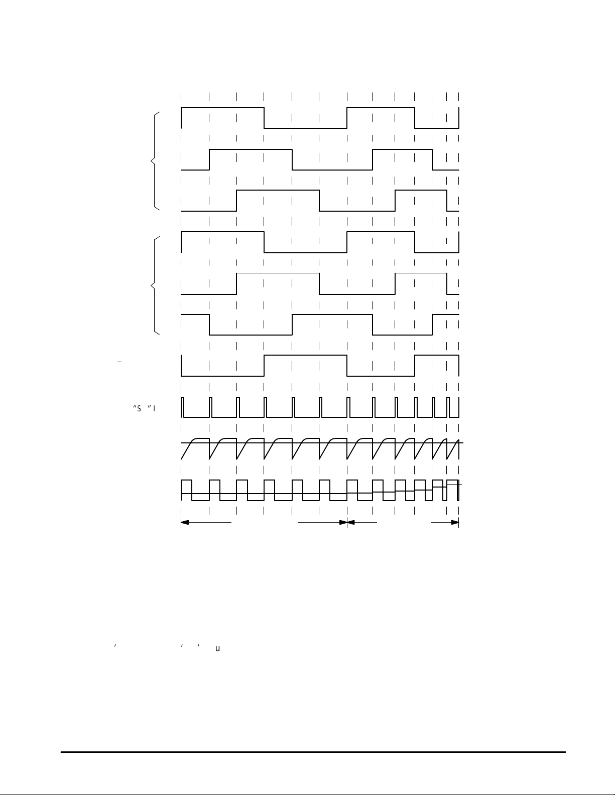
Figure 1. T ypical Three Phase, Six Step Motor Application
Rotor Electrical Position (Degrees)
24060 120 300 7206000
180 360 480
φ
A
φ
B
φ
C
φ
A
φ
B
φ
C
φA Output
Latch
I
SetI Input
RT/C
T
f
Output
out
Constant Motor Speed Increasing Motor
OPERA TING DESCRIPTION
The MC33039 provides an economical method of
implementing closed–loop speed control of brushless DC
motors by eliminating the need for a magnetic or optical
tachometer. Shown in the timing diagram of Figure 1, the
three inputs (Pins 1, 2, 3) monitor the brushless motor rotor
position sensors. Each sensor signal transition is digitally
detected, ORied at the Latch iSeti Input, and causes CT to
discharge. A corresponding output pulse is generated at f
(Pin 5) of a defined amplitude, and programmable width
determined by the values selected for RT and CT (Pin 6). The
average voltage of the output pulse train increases with
motor speed. When fed through a low pass filter or integrator,
a DC voltage proportional to speed is generated. Figure 2
shows the proper connections for a typical closed loop
out
≈
0.67 V
Speed
Vth
V
out
CC
(AVG)
application using the MC33035 brushless motor controller.
Constant speed operation down to 100 RPM is possible with
economical three phase four pole motors.
The φA inverter output (Pin 4) is used in systems where the
controller and motor sensor phasing conventions are not
compatible. A method of converting from either convention to
the other is shown in Figure 3. For a more detailed
explanation of this subject, refer to the text above Figure 39
on the MC33035 data sheet.
The output pulse amplitude VOH is constant with
temperature and controlled by the supply voltage on V
CC
(Pin 8). Operation down to 5.5 V is guaranteed over
temperature. For systems without a regulated power supply,
an internal 8.25 V shunt regulator is provided.
MOTOROLA ANALOG IC DEVICE DATA
3
Page 4

MC33039
Figure 2. T ypical Closed Loop Speed Control Application
N
Assy
Rotor
S
NS
Motor
Fault
M
V
POS
DEC
UVLO
+
+
REF
Output Buffers
+
Thermal
EA
–
+
R
–
PWM
–
+
LIMIT
I
Q
Q
S
S
+
R
Brake
OSC
MC33035P
Fwd/
Rev
CC
V
Enable
T
R
6
Set
Speed
C
T
5
15 k
–
+
2R
R
–
+
0.3 V
+
MC33039P
SQ
R
8.25 V
48
A
φ
Delay
Delay
Delay
20 k
3
2
1
4
MOTOROLA ANALOG IC DEVICE DATA
7
Page 5

MC33039
Figure 3. f
100
VCC = 6.25 V
°
C
TA = 25
10
1.0
0.1
, OUTPUT PULSE WIDTH (ms)
PW
t
0.01
2.0
Figure 5. f
+ 4.0
TA = 25°C
+ 2.0
, Pulse Width
out
versus Timing Resistor
CT = 220 nF
CT = 22 nF
CT = 2.2 nF
20 200
, Pulse Width Change
out
versus Supply V oltage
Figure 4. f
out
versus T emperature
+ 1.6
VCC = 6.25 V
RT = 10 k
+ 0.8
0
– 0.8
, OUTPUT PULSE WIDTH CHANGE (%)
PW
t
∆
– 1.6
– 55
CT = 22 nF
– 25 + 25 + 50 + 125+ 100+ 75
0
TA , AMBIENT TEMPERATURE (°C)RT , TIMING RESISTOR (kΩ)
Figure 6. Supply Current versus
Supply V oltage
20
16
Pins 1, 2, 3
Connected
together
, Pulse Width Change
0
– 2.0
, OUTPUT PULSE WIDTH CHANGE (%)
PW
t
∆
– 4.0
4.5
5.5 6.5 7.5 8.5
VCC , SUPPLY VOLTAGE (V)
Figure 7. f
versus Load Current
0
V
CC
– 2.0
Source Saturation
– 4.0
+ 0.4
+ 0.2
, OUTPUT SA TURATION VOLTAGE (V)
sat
V
0
0
(Load to Ground)
Sink Saturation
(Load to VCC)
Gnd
4.0 8.0 12 16
IO , OUTPUT LOAD CURRENT (mA)
, Saturation
out
VCC = 6.25 V
°
C
TA = 25
+16
+ 8.0
0
, SINK SATURATION CHANGE (%)
– 8.0
sat (sink)
V
–16
∆
12
8.0
, SUPPLY CURRENT (mA)
CC
I
4.0
0
0
∆
TA = –40°C
TA = 125°C
2.0 6.04.0 8.0 10
VCC , SUPPLY VOLTAGE (V)
Figure 8. f
, Saturation Change
out
versus T emperature
VCC = 6.25 V
IO = 5.0 mA
Sink Saturation
(Load to VCC)
0 + 125
+ 25– 25– 55
TA , AMBIENT TEMPERATURE (
∆
Source Saturation
(Load to Ground)
+ 50
TA = 25°C
+ 75 + 100
°
C)
+ 0.6
+ 0.4
+ 0.2
0
– 0.2
, SOURCE SATURATION CHANGE (%)
sat (SOURCE)
V
∆
MOTOROLA ANALOG IC DEVICE DATA
5
Page 6

NOTE 2
–T–
SEATING
PLANE
H
58
–B–
14
F
–A–
C
N
D
K
G
0.13 (0.005) B
M
T
MC33039
OUTLINE DIMENSIONS
P SUFFIX
PLASTIC PACKAGE
CASE 626–05
ISSUE K
L
J
M
M
A
M
NOTES:
1. DIMENSION L TO CENTER OF LEAD WHEN
FORMED PARALLEL.
2. PACKAGE CONTOUR OPTIONAL (ROUND OR
SQUARE CORNERS).
3. DIMENSIONING AND TOLERANCING PER ANSI
Y14.5M, 1982.
DIM MIN MAX MIN MAX
A 9.40 10.16 0.370 0.400
B 6.10 6.60 0.240 0.260
C 3.94 4.45 0.155 0.175
D 0.38 0.51 0.015 0.020
F 1.02 1.78 0.040 0.070
G 2.54 BSC 0.100 BSC
H 0.76 1.27 0.030 0.050
J 0.20 0.30 0.008 0.012
K 2.92 3.43 0.115 0.135
L 7.62 BSC 0.300 BSC
M ––– 10 ––– 10
N 0.76 1.01 0.030 0.040
INCHESMILLIMETERS
__
–T–
–A–
58
4X P
–B–
14
G
C
8X D
K
0.25 (0.010)MB
SEATING
PLANE
SS
A0.25 (0.010)MTB
D SUFFIX
PLASTIC PACKAGE
CASE 751–05
ISSUE N
(SO–8)
M
R
X 45
_
_
M
NOTES:
1. DIMENSIONING AND TOLERANCING PER
ANSI Y14.5M, 1982.
2. CONTROLLING DIMENSION: MILLIMETER.
3. DIMENSIONS A AND B DO NOT INCLUDE
MOLD PROTRUSION.
4. MAXIMUM MOLD PROTRUSION 0.15 (0.006)
PER SIDE.
5. DIMENSION D DOES NOT INCLUDE DAMBAR
PROTRUSION. ALLOWABLE DAMBAR
PROTRUSION SHALL BE 0.127 (0.005) TOTAL
IN EXCESS OF THE D DIMENSION AT
MAXIMUM MATERIAL CONDITION.
DIM MIN MAX MIN MAX
F
J
A 4.80 5.00 0.189 0.196
B 3.80 4.00 0.150 0.157
C 1.35 1.75 0.054 0.068
D 0.35 0.49 0.014 0.019
F 0.40 1.25 0.016 0.049
G 1.27 BSC 0.050 BSC
J 0.18 0.25 0.007 0.009
K 0.10 0.25 0.004 0.009
M 0 7 0 7
P 5.80 6.20 0.229 0.244
R 0.25 0.50 0.010 0.019
INCHESMILLIMETERS
____
6
MOTOROLA ANALOG IC DEVICE DATA
Page 7

MC33039
Motorola reserves the right to make changes without further notice to any products herein. Motorola makes no warranty , representation or guarantee regarding
the suitability of its products for any particular purpose, nor does Motorola assume any liability arising out of the application or use of any product or circuit, and
specifically disclaims any and all liability, including without limitation consequential or incidental damages. “T ypical” parameters which may be provided in Motorola
data sheets and/or specifications can and do vary in different applications and actual performance may vary over time. All operating parameters, including “Typicals”
must be validated for each customer application by customer’s technical experts. Motorola does not convey any license under its patent rights nor the rights of
others. Motorola products are not designed, intended, or authorized for use as components in systems intended for surgical implant into the body, or other
applications intended to support or sustain life, or for any other application in which the failure of the Motorola product could create a situation where personal injury
or death may occur. Should Buyer purchase or use Motorola products for any such unintended or unauthorized application, Buyer shall indemnify and hold Motorola
and its officers, employees, subsidiaries, affiliates, and distributors harmless against all claims, costs, damages, and expenses, and reasonable attorney fees
arising out of, directly or indirectly, any claim of personal injury or death associated with such unintended or unauthorized use, even if such claim alleges that
Motorola was negligent regarding the design or manufacture of the part. Motorola and are registered trademarks of Motorola, Inc. Motorola, Inc. is an Equal
Opportunity/Affirmative Action Employer.
MOTOROLA ANALOG IC DEVICE DATA
7
Page 8

MC33039
How to reach us:
USA/EUROPE/Locations Not Listed: Motorola Literature Distribution; JAPAN: Nippon Motorola Ltd.: SPD, Strategic Planning Office, 4–32–1,
P.O. Box 5405, Denver, Colorado 80217. 303–675–2140 or 1–800–441–2447 Nishi–Gotanda, Shinagawa–ku, Tokyo 141, Japan. 81–3–5487–8488
Mfax: RMFAX0@email.sps.mot.com – TOUCHTONE 602–244–6609 ASIA/ PACIFIC: Motorola Semiconductors H.K. Ltd.; 8B Tai Ping Industrial Park,
INTERNET: http://motorola.com/sps
8
– US & Canada ONLY 1–800–774–1848 51 Ting Kok Road, T ai Po, N.T., Hong Kong. 852–26629298
◊
MOTOROLA ANALOG IC DEVICE DATA
Mfax is a trademark of Motorola, Inc.
MC33039/D
 Loading...