

Page 1
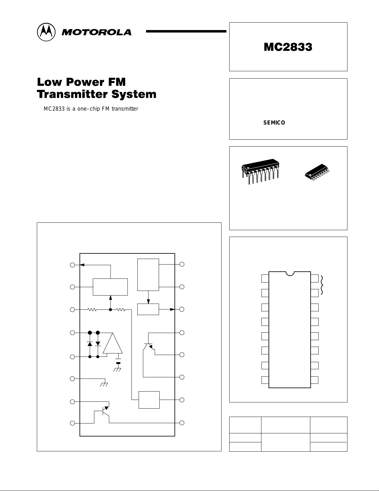
MC2833 is a one–chip FM transmitter subsystem designed for cordless
telephone and FM communication equipment. It includes a microphone
amplifier, voltage controlled oscillator and two auxiliary transistors.
• Wide Range of Operating Supply Voltage (2.8–9.0 V)
• Low Drain Current (I
• Low Number of External Parts Required
• – 30 dBm Power Output to 60 MHz Using Direct RF Output
• +10 dBm Power Output Attainable Using On–Chip Transistor Amplifiers
• Users Must Comply with Local Regulations on R.F.
Transmission (FCC, DOT, P.T.T., etc)
= 2.9 mA Typ)
CC
Order this document by MC2833/D
LOW POWER
FM TRANSMITTER
SYSTEM
SEMICONDUCTOR
TECHNICAL DATA
P SUFFIX
PLASTIC PACKAGE
CASE 648
D SUFFIX
PLASTIC PACKAGE
CASE 751B
(SO–16)
Representative Block Diagram
PIN CONNECTIONS
1
RF
Osc
2
3
4
5
6
Variable
Reactance
Buffer
Mic
Amp
+–
16
15
14
13
12
11
Variable
Reactance
Output
Decoupling
Modulator
Input
Mic Amp
Output
Mic Amp
Input
Gnd
Tr 1
Emitter
Tr 1
Base
1
2
3
4
5
6
7
8
16
15
14
13
12
11
10
Tr 2
9
RF
Osc
RF
Output
Base
Tr 2
Emitter
Tr 2
Collector
V
CC
Tr 1
Collector
7
8
MOTOROLA ANALOG IC DEVICE DATA
V
REF
10
9
ORDERING INFORMATION
Operating
Device
MC2833D
MC2833P
Motorola, Inc. 1996 Rev 1
Temperature Range
TA = – 30 to +75°C
Package
SO–16
Plastic DIP
1
Page 2
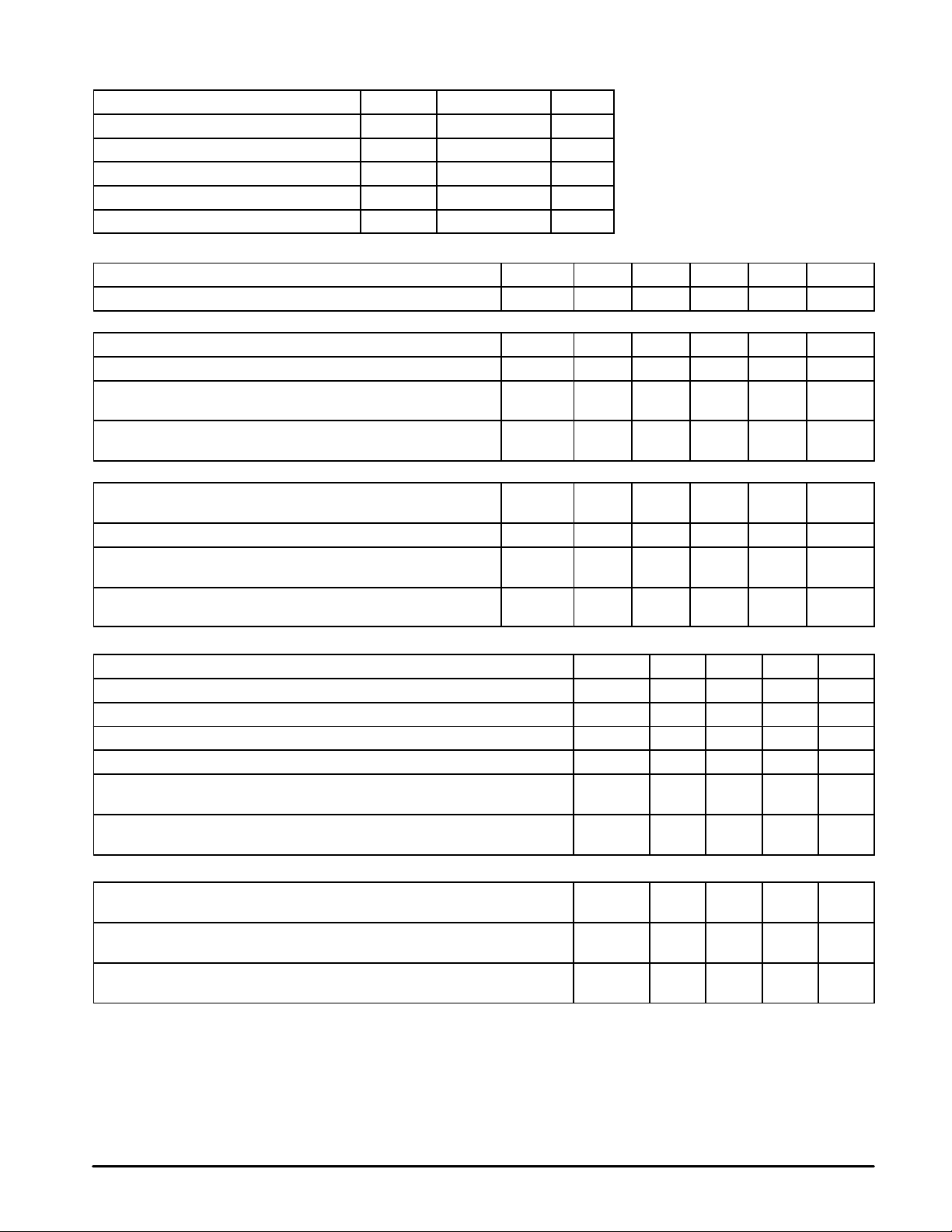
MAXIMUM RATINGS
Ratings Symbol Value Unit
Power Supply Voltage V
Operating Supply Voltage Range V
Junction Temperature T
Operating Ambient Temperature T
Storage Temperature Range T
CC
CC
A
stg
MC2833
10 (max) V
2.8–9.0 V
J
+ 150 °C
– 30 to + 75 °C
– 65 to + 150 °C
ELECTRICAL CHARACTERISTICS (V
Characteristics
Drain Current (No input signal) I
FM MODULATOR
Output RF Voltage (fo = 16.6 MHz) V
Output DC Voltage (No input signal) Vdc 14 2.2 2.5 2.8 V
Modulation Sensitivity (fo = 16.6 MHz)
Modulation Sensitivity (Vin = 0.8 V to 1.2 V)
Maximum Deviation (fo = 16.6 MHz)
Maximum Deviation (Vin = 0 V to 2.0 V)
MIC AMPLIFIER
Closed Loop Voltage Gain (Vin = 3.0 mVrms)
Closed Loop Voltage Gain (fin = 1.0 kHz)
Output DC Voltage (No input signal) V
Output Swing Voltage (Vin = 30 mVrms)
Output Swing Voltage (fin = 1.0 kHz)
Total Harmonic Distortion (Vin = 3.0 mVrms)
Total Harmonic Distortion (fin = 1.0 kHz)
= 4.0 V, TA = 25°C, unless otherwise noted)
CC
Symbol Pin Min Typ Max Unit
CC
RF 14 60 90 130 mVrms
out
SEN 3
Fdev 3
A
v
dc 4 1.1 1.4 1.7 V
out
V
p–p 4 0.8 1.2 1.6 Vp–p
out
THD 4 – 0.15 2.0 %
10 1.7 2.9 4.3 mA
14
14
7.0
–
3.0
–
4
5
27
–
10
5.0
30
15
–
–
–
Hz/mVdc
–
10
–
33
–
AUXILIARY TRANSISTOR STATIC CHARACTERISTICS
Characteristics Symbol Min Typ Max Unit
Collector Base Breakdown Voltage (IC = 5.0 µA) V
Collector Emitter Breakdown Voltage (IC = 200 µA) V
Collector Substrate Breakdown Voltage (IC = 50 µA) V
Emitter Base Breakdown Voltage (IE = 50 µA) V
Collector Base Cut Off Current (VCB = 10 V)
Collector Base Cut Off Current (IE = 0)
DC Current Gain (IC = 3.0 mA)
DC Current Gain (VCE = 3.0 V)
(BR)CBO
(BR)CEO
(BR)CSO
(BR)EBO
I
CBO
h
FE
15 45 – V
10 15 – V
– 70 – V
– 6.2 – V
– – 200 nA
40 150 – –
kHz
dB
AUXILIARY TRANSISTOR DYNAMIC CHARACTERISTICS
Current Gain Bandwidth Product (VCE = 3.0 V)
Current Gain Bandwidth Product (IC = 3.0 mA)
Collector Base Capacitance (VCE = 3.0 V)
Collector Base Capacitance (IC = 0)
Collector Substrate Capacitance (VCS = 3.0 V)
Collector Substrate Capacitance (IC = 0)
2
f
T
C
CB
C
CS
– 500 – MHz
– 2.0 – pF
– 3.3 – pF
MOTOROLA ANALOG IC DEVICE DATA
Page 3
Mod In
Mod Out
0.0047
MC2833
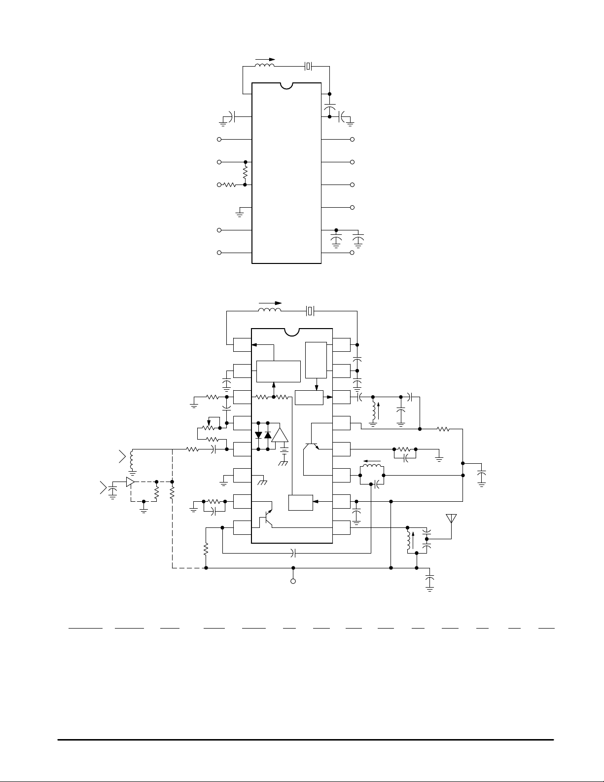
Figure 1. T est Circuit
µ
H
5.1
1
µ
F
2
3
16.605 MHz
16
15
14
68 pF
39 pF
RF Out
Crystal:
f
= 16.605 MHz
o
C
= 30 pF
L
C
= 6.1 pF
o
R
= 10 Ω Max
S
Mic Amp
Out
Mic Amp
Emitter 1
Base 1
In
6.3 k
4
220 k
MC2833
5
6
7
89
13
12
11
10
+
47
µ
F
Base 2
Emitter 2
Collector 2
0.01
Collector 1
µ
F
Figure 2. Single Chip VHF Narrowband FM Transmitter
X1Lt
1
Variable
2
Reactance
3
4
Mic Amp
Buffer
+–
5
µ
Q2
6
7
V
REF
Q1
8
Cc2
= 9.0 Vdc
V
CC
Audio
Input
Deviation
Adjust
Dynamic
Mike
1.0 k
Electret
(alternate)
Microphone
and biasing
120 k
4.7 k
100 k
2.7 k
Rb1
4700 p
100 k
4700 p
1.0
Re1
470 p
NOTES:
1. Components versus output frequency:
Output RF
49.7 MHz
76 MHz
144.6 MHz
X1 (MHz) Lt (µH) L1 (µH) L2 (µH) Re1 Rb1 Cc1 Cc2 C1 C2 C3 C4 C5
16.5667
12.6000
12.05
3.3–4.7
5.1
5.6
0.22
0.22
0.15
0.22
0.22
0.10
330
150
150
2. Crystal X1 is fundamental mode, calibrated for parallel resonance with a 32 pF load. The final output frequency is generated by frequency multiplication within
2. the MC2833 IC. The RF output buffer (Pin 14) and Q2 transistor are used as a frequency tripler and doubler, respectively, in the 76 and 144.6 MHz transmitters.
2. The Q1 output transistor is a linear amplifier in the 49.7 MHz and 76 MHz transmitters, and a frequency doubler in the 144.6 MHz transmitter.
3. All coils used are 7 mm shielded inductors, CoilCraft series M1 175A, M1282A–M1289A, M1312A or equivalent.
4. Power output is ≈ + 10 dBm for 49.7 MHz and 76 MHz transmitters, and ≈ + 5.0 dBm for the 144.6 MHz transmitter at VCC = 8.0 V. Power output drops with
4. lower VCC.
5. All capacitors in microfarads, inductors in Henries and resistors in Ohms unless otherwise specified.
6. Other frequency combinations may be set–up by simple scaling of the 3 examples shown.
RF
Osc.
390 k
300 k
220 k
16
15
14
13
12
11
10
470 p
9
33 p
68 p
47 p
47 p
56 p
51 p
L1
C3
0.22
33 p
10 p
10 p
Cc1
C1
µ
390 k
1.0 k
C2
C4
L2
C5
1000 p
RF Output
5.0 to 10 dBm
(see Note 4)
+
µ
F
1.0
tantalum
33 p
68 p
68 p
470 p
470 p
1000 p
33 p
12 p
18 p
47 p
20 p
12 p
220 p
120 p
33 p
MOTOROLA ANALOG IC DEVICE DATA
3
Page 4
MC2833
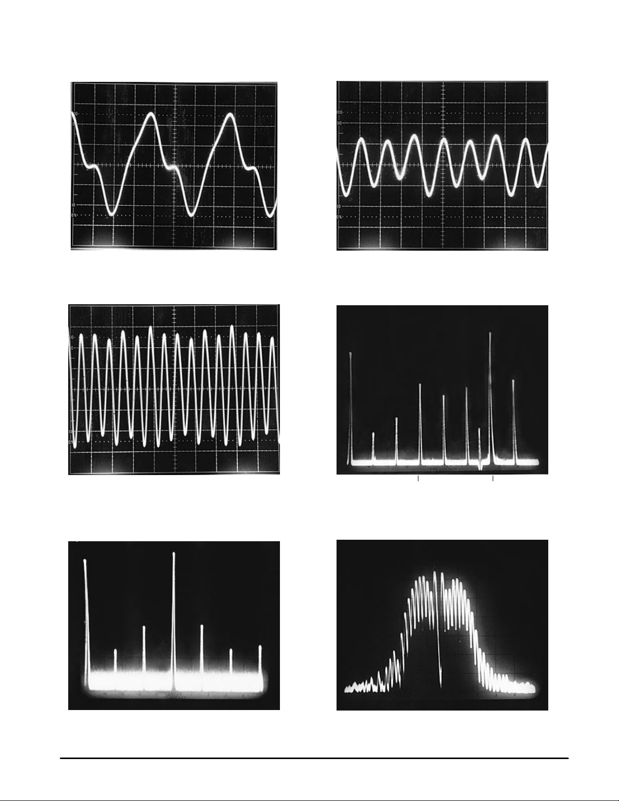
Figure 3. Buffer/Multiplier (x3, Pin 14)
(16 MHz Fundamental)
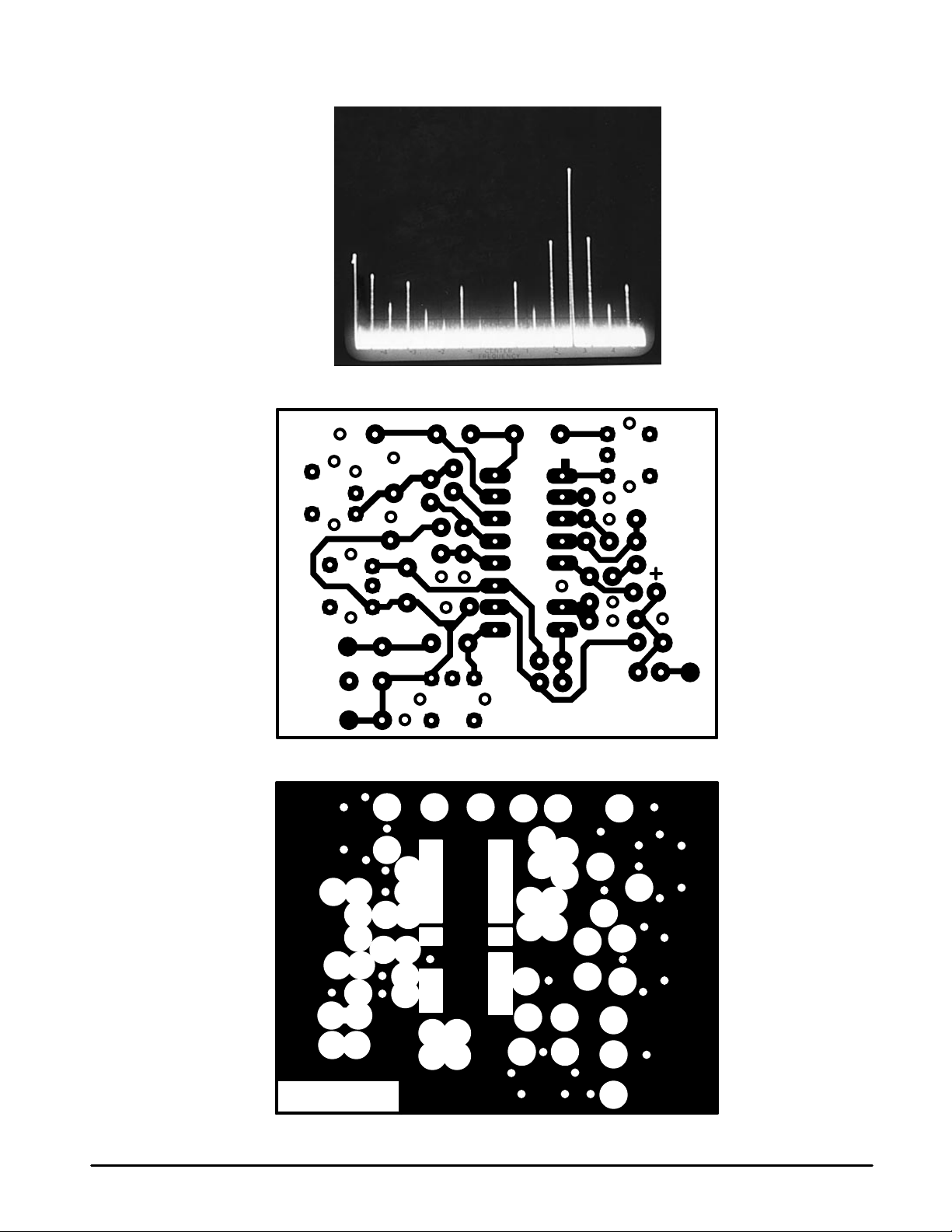
Figure 5. Doubler Output 76 MHz (Pin 11) Figure 6. Spectrum
Figure 4. Input to Doubler (Pin 13)
(49.7 MHz x 3 Component)
Figure 7. Output Spectrum (49.7 MHz)
4
38 MHz 76 MHz
Figure 8. Modulation Spectrum
(1.0 kHz Showing Carrier Null)
– 43 dB
MOTOROLA ANALOG IC DEVICE DATA
Page 5
MC2833
Figure 9. 144.6 MHz/x12 Multiplier
Figure 10. Circuit Side View
OUT
GND
VCC
Figure 11. Ground Plane on Component Side
IN
MC2833P
MC2833P
MOTOROLA ANALOG IC DEVICE DATA
5
Page 6
MC2833
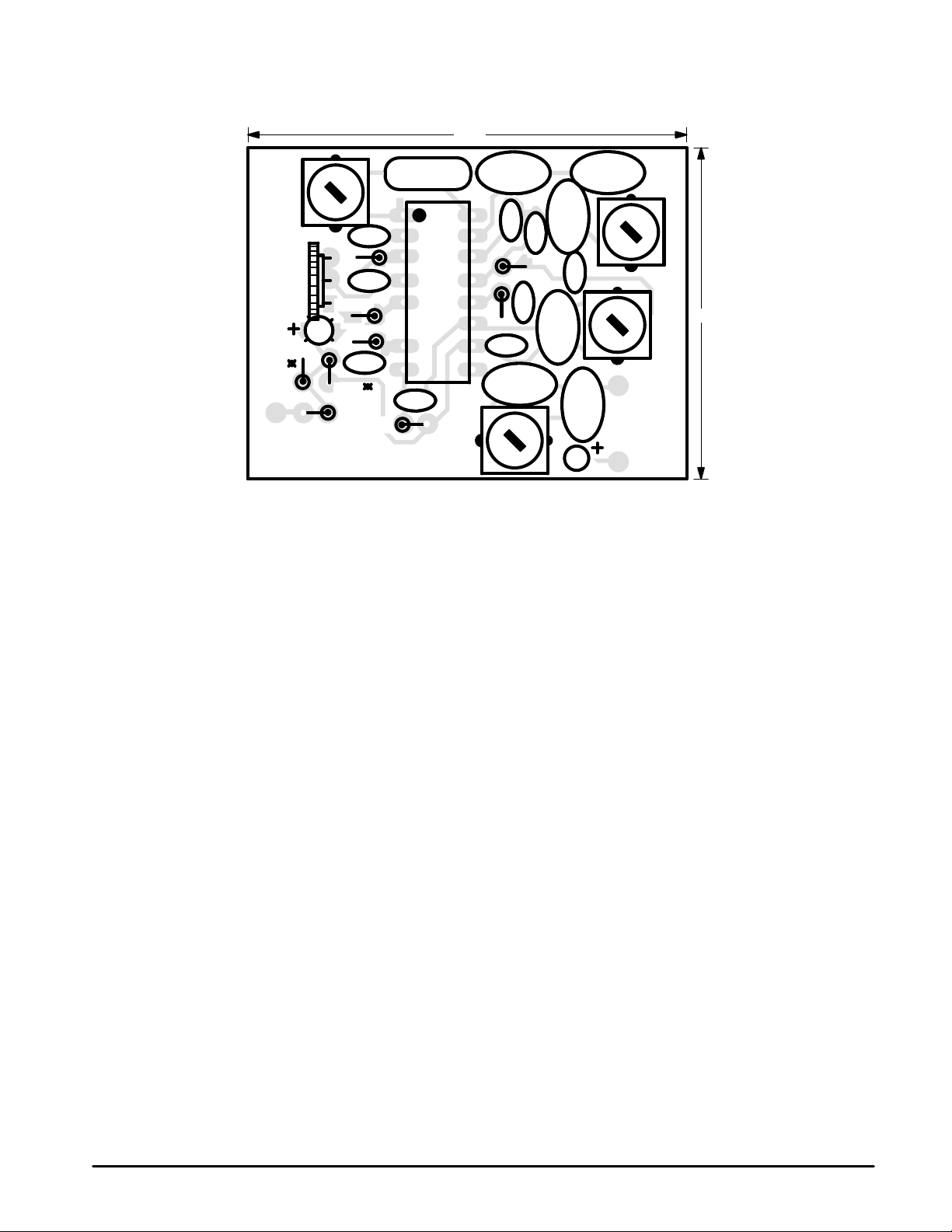
Figure 12. Component View
2.0
″
Lt
X1 XTAL
4.7 Kp
100K
100K
1K
1.0
2.7K
4.7 Kp
120K
Re1
470p
4.7 K
Cc2
Rb1
MC2833P
NOTES: • Positive artwork provided.
• Drill holes must be plated to ensure making all ground (VEE) connections!
• Resistors labelled * are used for biasing of electret microphone if used.
• Capacitors labelled ″SM″ are silver mica.
• Final board size 1.5″ × 2.0″.
56p
SM
MC2833P
1K
470p
C4
SM
47p
390K
C2
L2
Cc1
C3
C1
1.0
SM
1Kp
SM
C5
51p
SM
SM
L1
µ
.22 H
1.5
″
6
MOTOROLA ANALOG IC DEVICE DATA
Page 7
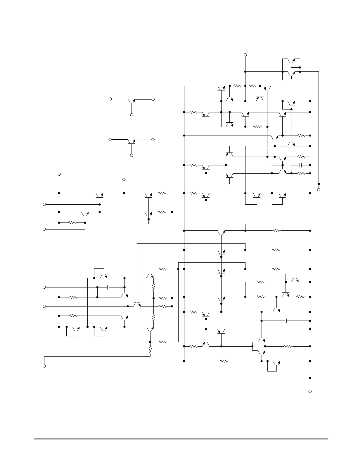
Figure 13. Circuit Schematic
Pin 9 Pin 7
MC2833
Pin 4
50 50
820
Pin 15
Pin16
Pin 1
Pin 2
Pin 10
10 k
2.2 k
2.2 k
Pin 8
Pin 11 Pin 12
Pin 13
Pin 14
120
120
520
470
4.7 k
570
610
15 k
570
2.2 k
15 k
8.5 k
20.2 k
24 k
6.8 k
6.8 k
Pin 5
18 k
18 k
18 k
9.7 k
Pin 3
MOTOROLA ANALOG IC DEVICE DATA
8 k
4.7 k
2.2 k
18 k
56 k
Pin 6
7
Page 8
–T–
MC2833
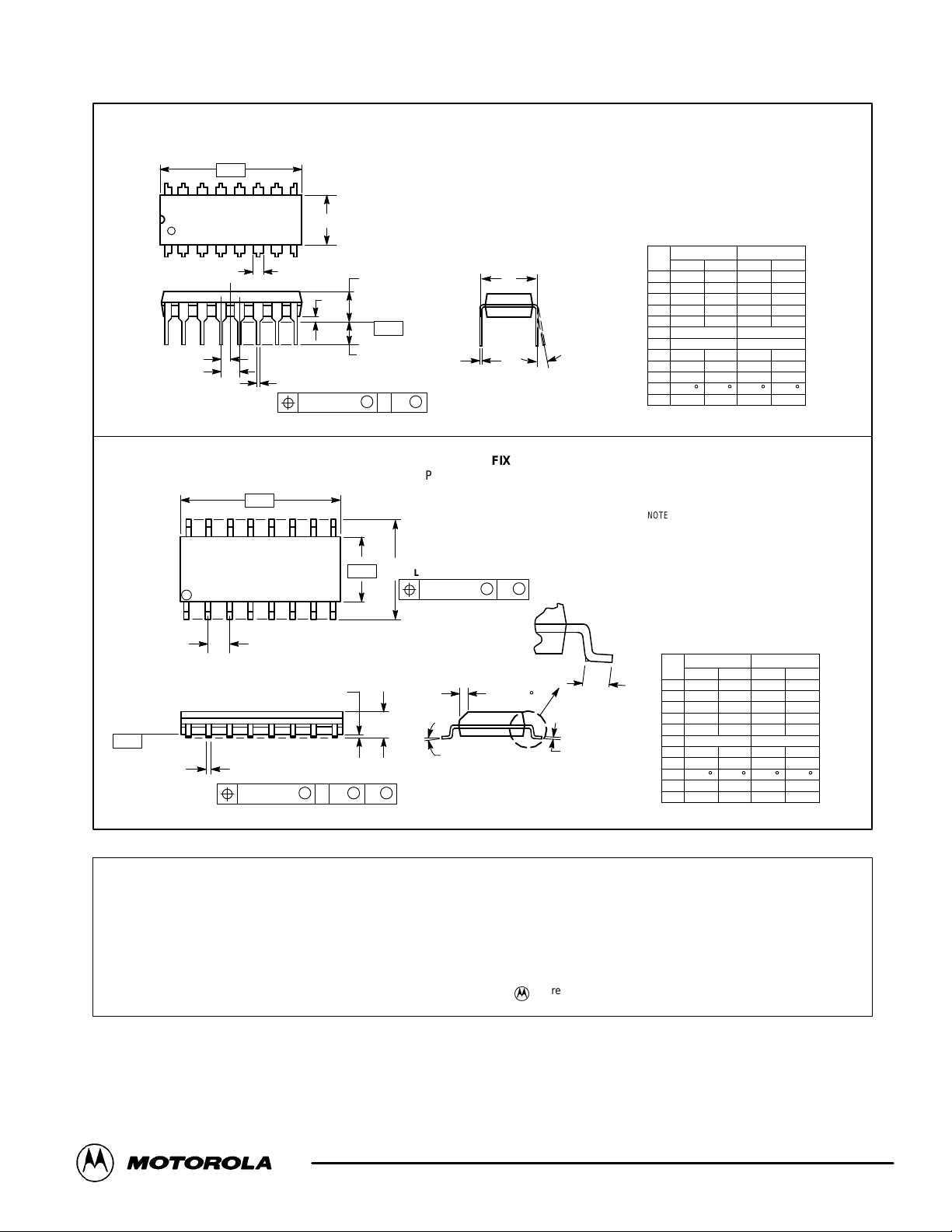
OUTLINE DIMENSIONS
PLASTIC PACKAGE
–A–
916
B
18
F
C
S
–T–
H
G
D
16 PL
0.25 (0.010) T
K
M
–A–
16 9
–B–
18
G
K
C
SEATING
PLANE
D
16 PL
0.25 (0.010) A
M
S
B
T
S
CASE 648–08
SEATING
PLANE
M
A
PLASTIC PACKAGE
CASE 751B–05
8 PLP
0.25 (0.010) B
M
P SUFFIX
ISSUE R
J
D SUFFIX
(SO–16)
ISSUE J
M
NOTES:
1. DIMENSIONING AND TOLERANCING PER ANSI
Y14.5M, 1982.
2. CONTROLLING DIMENSION: INCH.
3. DIMENSION L TO CENTER OF LEADS WHEN
FORMED PARALLEL.
4. DIMENSION B DOES NOT INCLUDE MOLD FLASH.
5. ROUNDED CORNERS OPTIONAL.
DIM MIN MAX MIN MAX
L
M
S
R
X 45
_
F
J
A 0.740 0.770 18.80 19.55
B 0.250 0.270 6.35 6.85
C 0.145 0.175 3.69 4.44
D 0.015 0.021 0.39 0.53
F 0.040 0.70 1.02 1.77
G 0.100 BSC 2.54 BSC
H 0.050 BSC 1.27 BSC
J 0.008 0.015 0.21 0.38
K 0.110 0.130 2.80 3.30
L 0.295 0.305 7.50 7.74
M 0 10 0 10
S 0.020 0.040 0.51 1.01
NOTES:
1. DIMENSIONING AND TOLERANCING PER ANSI
Y14.5M, 1982.
2. CONTROLLING DIMENSION: MILLIMETER.
3. DIMENSIONS A AND B DO NOT INCLUDE
MOLD PROTRUSION.
4. MAXIMUM MOLD PROTRUSION 0.15 (0.006)
PER SIDE.
5. DIMENSION D DOES NOT INCLUDE DAMBAR
PROTRUSION. ALLOWABLE DAMBAR
PROTRUSION SHALL BE 0.127 (0.005) TOTAL
IN EXCESS OF THE D DIMENSION AT
MAXIMUM MATERIAL CONDITION.
DIM MIN MAX MIN MAX
A 9.80 10.00 0.386 0.393
B 3.80 4.00 0.150 0.157
C 1.35 1.75 0.054 0.068
D 0.35 0.49 0.014 0.019
F 0.40 1.25 0.016 0.049
G 1.27 BSC 0.050 BSC
J 0.19 0.25 0.008 0.009
K 0.10 0.25 0.004 0.009
M 0 7 0 7
P 5.80 6.20 0.229 0.244
R 0.25 0.50 0.010 0.019
MILLIMETERSINCHES
____
INCHESMILLIMETERS
____
Motorola reserves the right to make changes without further notice to any products herein. Motorola makes no warranty , representation or guarantee regarding
the suitability of its products for any particular purpose, nor does Motorola assume any liability arising out of the application or use of any product or circuit, and
specifically disclaims any and all liability, including without limitation consequential or incidental damages. “T ypical” parameters which may be provided in Motorola
data sheets and/or specifications can and do vary in different applications and actual performance may vary over time. All operating parameters, including “Typicals”
must be validated for each customer application by customer’s technical experts. Motorola does not convey any license under its patent rights nor the rights of
others. Motorola products are not designed, intended, or authorized for use as components in systems intended for surgical implant into the body, or other
applications intended to support or sustain life, or for any other application in which the failure of the Motorola product could create a situation where personal injury
or death may occur. Should Buyer purchase or use Motorola products for any such unintended or unauthorized application, Buyer shall indemnify and hold Motorola
and its officers, employees, subsidiaries, affiliates, and distributors harmless against all claims, costs, damages, and expenses, and reasonable attorney fees
arising out of, directly or indirectly, any claim of personal injury or death associated with such unintended or unauthorized use, even if such claim alleges that
Motorola was negligent regarding the design or manufacture of the part. Motorola and are registered trademarks of Motorola, Inc. Motorola, Inc. is an Equal
Opportunity/Affirmative Action Employer.
Mfax is a trademark of Motorola, Inc.
How to reach us:
USA/EUROPE/Locations Not Listed: Motorola Literature Distribution; JAPAN: Nippon Motorola Ltd.; Tatsumi–SPD–JLDC, 6F Seibu–Butsuryu–Center,
P.O. Box 5405, Denver, Colorado 80217. 303–675–2140 or 1–800–441–2447 3–14–2 Tatsumi Koto–Ku, Tokyo 135, Japan. 81–3–3521–8315
Mfax: [email protected] – TOUCHTONE 602–244–6609 ASIA/PACIFIC: Motorola Semiconductors H.K. Ltd.; 8B Tai Ping Industrial Park,
– US & Canada ONLY 1–800–774–1848 51 Ting Kok Road, T ai Po, N.T., Hong Kong. 852–26629298
INTERNET: http://www.mot.com/SPS/
8
◊
MOTOROLA ANALOG IC DEVICE DATA
MC2833/D
 Loading...