

Page 1
SEMICONDUCTOR
TECHNICAL DATA
QUAD EIA–422/3 LINE
RECEIVER WITH
THREE–STATE OUTPUTS
ORDERING INFORMATION
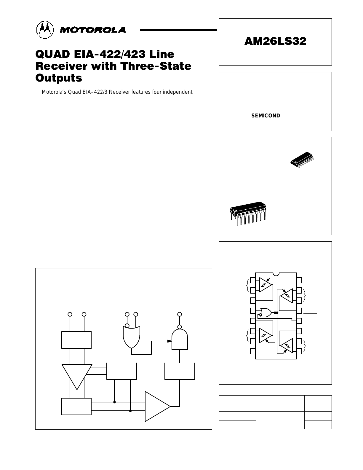
PIN CONNECTIONS
Order this document by AM26LS32/D
PC SUFFIX
PLASTIC PACKAGE
CASE 648
D SUFFIX
PLASTIC PACKAGE
CASE 751B
(SO–16)
Device
Operating
Temperature Range
Package
AM26LS32PC
MC26LS32D*
TA = 0 to 70°C
Plastic DIP
SO–16
9
–
+
–
8
7
6
5
4
3
2
1
10
11
12
13
14
+
–
+
–
Inputs A
+
V
CC
16
3–State
Control
GND
Output B
Output D
15
3–State
Control
Inputs C
Inputs B
Inputs D
Outputs A
Output C
1
MOTOROLA ANALOG IC DEVICE DATA
Motorola′s Quad EIA–422/3 Receiver features four independent receiver
chains which comply with EIA Standards for the Electrical Characteristics of
Balanced/Unbalanced Voltage Digital Interface Circuits. Receiver outputs
are 74LS compatible, three–state structures which are forced to a high
impedance state when Pin 4 is a Logic “0” and Pin 12 is a Logic “1.” A PNP
device buffers each output control pin to assure minimum loading for either
Logic “1” or Logic “0” inputs. In addition, each receiver chain has internal
hysteresis circuitry to improve noise margin and discourage output instability
for slowly changing input waveforms. A summary of AM26LS32 features
include:
• Four Independent Receiver Chains
• Three–State Outputs
• High Impedance Output Control Inputs
(PIA Compatible)
• Internal Hysteresis – 30 mV (Typical) @ Zero Volts Common Mode
• Fast Propagation Times – 25 ns (Typical)
• TTL Compatible
• Single 5.0 V Supply Voltage
• Fail–Safe Input–Output Relationship. Output Always High When Inputs
Are Open, Terminated or Shorted
• 6.0 k Minimum Input Impedance
* Note that the surface mount MC26LS32D device uses the same die as in the plastic DIP
* AM26LS32DC device, but with an MC prefix to prevent confusion with the package suffix.
Representative Block Diagram
Hysteresis
Amplifier
Amplifier
Three–State
Control
Inputs
Output
Differential
Inputs
Input
Network
Level
Translator
Level
Translator
Motorola, Inc. 1995
Page 2
AM26LS32
2
MOTOROLA ANALOG IC DEVICE DATA
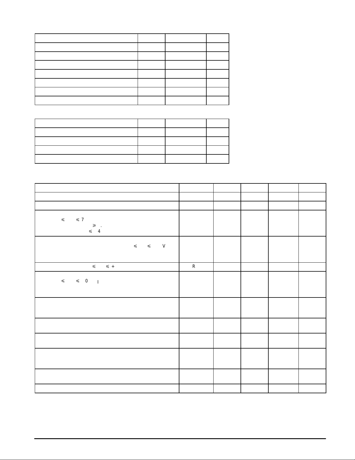
MAXIMUM RATINGS
Rating Symbol Value Unit
Power Supply Voltage V
CC
7.0 Vdc
Input Common Mode Voltage V
ICM
± 25 Vdc
Input Differential Voltage V
ID
± 25 Vdc
Three–State Control Input Voltage V
I
7.0 Vdc
Output Sink Current I
O
50 mA
Storage Temperature T
stg
– 65 to + 150 °C
Operating Junction Temperature T
J
+ 150 °C
RECOMMENDED OPERATING CONDITIONS
Rating Symbol Value Unit
Power Supply Voltage V
CC
4.75 to 5.25 Vdc
Operating Ambient Temperature T
A
0 to + 70 °C
Input Common Mode Voltage Range V
ICR
– 7.0 to + 7.0 Vdc
Input Differential Voltage Range V
IDR
6.0 Vdc
ELECTRICAL CHARACTERISTICS (Unless otherwise noted, minimum and maximum limits apply over recommended temperature
and power supply voltage ranges. Typical values are for TA = 25°C, VCC = 5.0 V and VIC = 0 V. See Note 1.)
Characteristic
Symbol Min Typ Max Unit
Input Voltage – High Logic State (Three–State Control) V
IH
2.0 – – V
Input Voltage – Low Logic State (Three–State Control) V
IL
– – 0.8 V
Differential Input Threshold Voltage (Note 2)
(–7.0 V p VIC p 7.0 V, VIH = 2.0 V)
(IO = –0.4 mA, VOH q 2.7 V)
(IO = 8.0 mA, VOL p 0.45 V)
V
TH(D)
–
–
–
–
0.2
–0.2
V
Input Bias Current
(VCC = 0 V or 5.25) (Other Inputs at –15 V p Vin p +15 V)
Vin = +15 V
Vin = –15 V
I
IB(D)
–
–
–
–
2.3
–2.8
mA
Input Resistance ( –15 V p Vin p +15 V) R
in
6.0 K – – Ohms
Input Balance and Output Level
(–7.0 V p VIC p 7.0 V, VIH = 2.0 V, See Note 3)
(IO = –0.4 mA, VID = 0.4 V)
(IO = 8.0 mA, VID = –0.4 V)
V
OH
V
OL
2.7
–
–
–
–
0.45
V
Output Third State Leakage Current
(V
I(D)
= + 3.0 V, VIL = 0.8 V, VO = 0.4 V)
(V
I(D)
= – 3.0 V, VIL = 0.8 V, VO = 2.4 V)
I
OZ
–
–
–
–
–20
20
µA
Output Short Circuit Current
(V
I(D)
= 3.0 V, VIH = 2.0 V, VO = 0 V, See Note 4)
I
OS
–15 – –85 mA
Input Current – Low Logic State (Three–State Control)
(VIL = 0.4 V)
I
IL
– – –360 µA
Input Current – High Logic State (Three–State Control)
(VIH = 2.7 V)
(VIH = 5.5 V)
I
IH
–
–
–
–
20
100
µA
Input Clamp Diode Voltage (Three–State Control)
(IIC = –18 mA)
V
IK
– – –1.5 V
Power Supply Current (VIL = 0 V) (All Inputs Grounded) I
CC
– – 70 mA
NOTES: 1.All currents into device pins are shown as positive, out of device pins are negative. All voltages referenced to ground unless otherwise noted.
2.Differential input threshold voltage and guaranteed output levels are done simultaneously for worst case.
3.Refer to EIA–422/3 for exact conditions. Input balance and guaranteed output levels are done simultaneously for worst case.
4.Only one output at a time should be shorted.
Page 3

AM26LS32
3
MOTOROLA ANALOG IC DEVICE DATA
SWITCHING CHARACTERISTICS (V
CC
= 5.0 V and TA = 25°C, unless otherwise noted)
Characteristic
Symbol Min Typ Max Unit
Propagation Delay Time – DIfferential Inputs to Output
(Output High to Low)
(Output Low to High)
t
PHL(D)
t
PLH(D)
–
–
–
–
30
30
ns
Propagation Delay Time – Three–State Control to Output
(Output Low to Third State)
(Output High to Third State)
(Output Third State to High)
(Output Third State to Low)
t
PLZ
t
PHZ
t
PZH
t
PZL
–
–
–
–
–
–
–
–
35
35
30
30
ns
Figure 1. Switching Test Circuit and Wave for Propagation Delay Differential Input to Output
– 2.5 V
V
OL
Output
+ 2.0 V0 V 3–State Control
CL = 15 pF
(Includes Probe
and Stray
Capacitance)
1.3 V1.3 V
0 V
t
PHL(D)
0 V
V
OH
t
PLH(D)
0 VInput
+ 2.5 V
–
+
Differential
Inputs
51
Pulse
Generator
To Scope
(Input)
To Scope
(Output)
Input Pulse Characteristics
t
TLH
– t
THL
– 6.0 ns (10% to 90%)
PRR – 1.0 MHz, 50% Duty Cycle
To Scope
(Output)
5.0 k
+
–
Differential
Inputs
3–State
Control
2.0 V
51
SW2
+ 5.0 V2.0 k
SW1
Pulse
Generator
To Scope
(Input)
+ 1.5 V for t
PHZ
and t
PZH
– 1.5 V for t
PLZ
and t
PZL
All Diodes 1N916 or
Equivalent
Input Pulse Characteristics
t
TLH
– t
THL
– 6.0 ns (10% to 90%)
PRR – 1.0 MHz, 50% Duty Cycle
CL 15 pF
(Includes
Probe and Stray
Capacitance)
t
PHZ
0 V
[
5.0 V – V
BE
V
OL
3.0 V
Input
Output
[
1.3 V
t
PZL
3.0 V
1.5 V
SW1 Closed
SW2 Closed
SW1 Closed
SW2 Closed
0 V
Input
Output
t
PZL
SW1 Closed
SW2 Open
1.5 V
1.5 V
0.5 V
t
PHZ
SW1 Open
SW2 Closed
0 V
1.5 V
t
PZH
1.5 V
t
PZH
Input
3.0 V
0 V
V
OH
Output
0 V
1.5 V
Output
Input
0 V
t
PLZ
V
OH
V
OL
[
1.3 V
3.0 V
0.5 V
0 V
0 V
t
PLZ
Figure 2. Propagation Delay Three–State Control Input to Output
Page 4
AM26LS32
4
MOTOROLA ANALOG IC DEVICE DATA
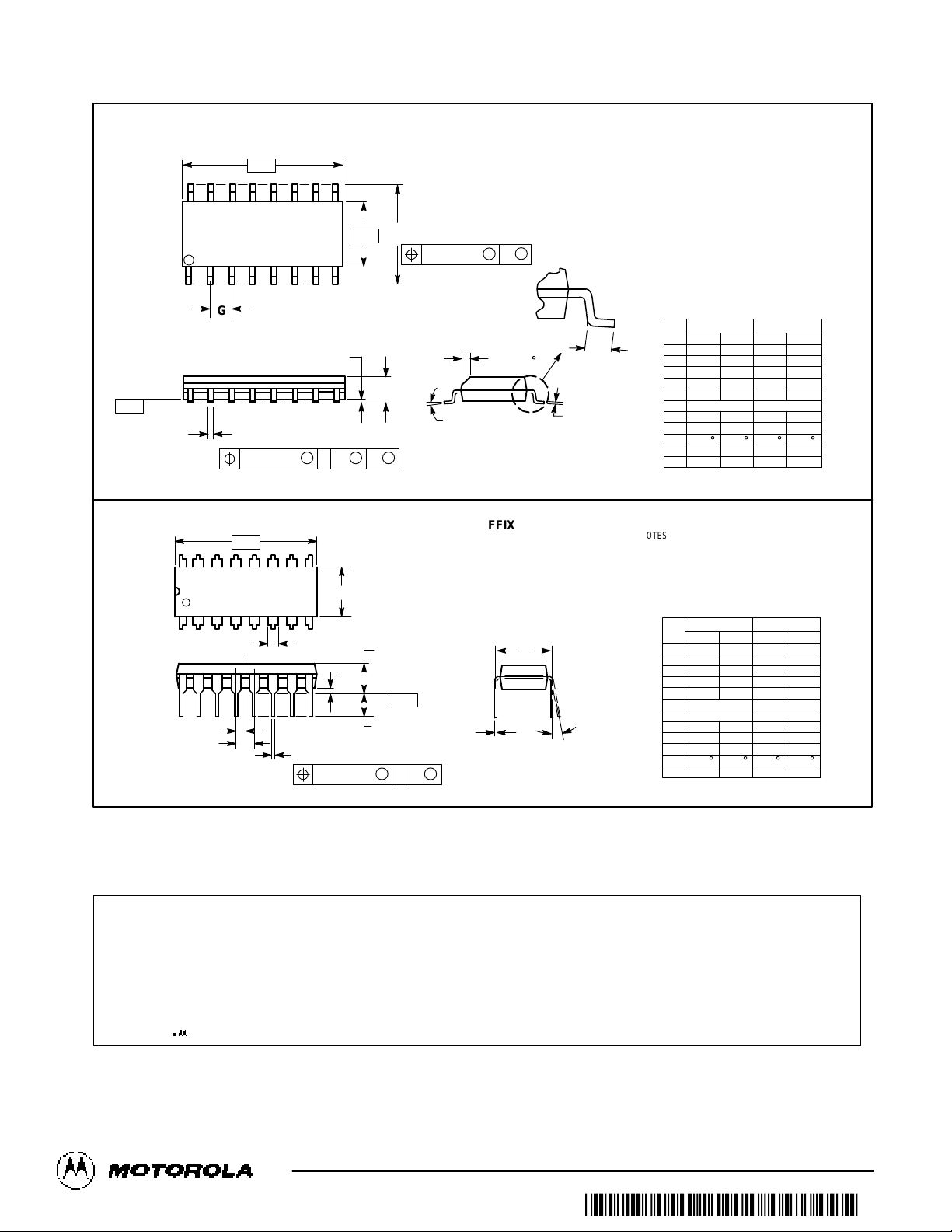
OUTLINE DIMENSIONS
NOTES:
1. DIMENSIONING AND TOLERANCING PER ANSI
Y14.5M, 1982.
2. CONTROLLING DIMENSION: MILLIMETER.
3. DIMENSIONS A AND B DO NOT INCLUDE
MOLD PROTRUSION.
4. MAXIMUM MOLD PROTRUSION 0.15 (0.006)
PER SIDE.
5. DIMENSION D DOES NOT INCLUDE DAMBAR
PROTRUSION. ALLOWABLE DAMBAR
PROTRUSION SHALL BE 0.127 (0.005) TOTAL
IN EXCESS OF THE D DIMENSION AT
MAXIMUM MATERIAL CONDITION.
1 8
16 9
SEATING
PLANE
F
J
M
R
X 45
_
G
8 PLP
–B–
–A–
M
0.25 (0.010) B
S
–T–
D
K
C
16 PL
S
B
M
0.25 (0.010) A
S
T
DIM MIN MAX MIN MAX
INCHESMILLIMETERS
A 9.80 10.00 0.386 0.393
B 3.80 4.00 0.150 0.157
C 1.35 1.75 0.054 0.068
D 0.35 0.49 0.014 0.019
F 0.40 1.25 0.016 0.049
G 1.27 BSC 0.050 BSC
J 0.19 0.25 0.008 0.009
K 0.10 0.25 0.004 0.009
M 0 7 0 7
P 5.80 6.20 0.229 0.244
R 0.25 0.50 0.010 0.019
_ _ _ _
NOTES:
1. DIMENSIONING AND TOLERANCING PER ANSI
Y14.5M, 1982.
2. CONTROLLING DIMENSION: INCH.
3. DIMENSION L TO CENTER OF LEADS WHEN
FORMED PARALLEL.
4. DIMENSION B DOES NOT INCLUDE MOLD FLASH.
5. ROUNDED CORNERS OPTIONAL.
–A–
B
F
C
S
H
G
D
J
L
M
16 PL
SEATING
1 8
916
K
PLANE
–T–
M
A
M
0.25 (0.010) T
DIM MIN MAX MIN MAX
MILLIMETERSINCHES
A 0.740 0.770 18.80 19.55
B 0.250 0.270 6.35 6.85
C 0.145 0.175 3.69 4.44
D 0.015 0.021 0.39 0.53
F 0.040 0.70 1.02 1.77
G 0.100 BSC 2.54 BSC
H 0.050 BSC 1.27 BSC
J 0.008 0.015 0.21 0.38
K 0.110 0.130 2.80 3.30
L 0.295 0.305 7.50 7.74
M 0 10 0 10
S 0.020 0.040 0.51 1.01
____
PC SUFFIX
PLASTIC PACKAGE
CASE 648–08
ISSUE R
D SUFFIX
PLASTIC PACKAGE
CASE 751B–05
(SO–16)
ISSUE J
Motorola reserves the right to make changes without further notice to any products herein. Motorola makes no warranty , representation or guarantee regarding
the suitability of its products for any particular purpose, nor does Motorola assume any liability arising out of the application or use of any product or circuit,
and specifically disclaims any and all liability, including without limitation consequential or incidental damages. “T ypical” parameters can and do vary in different
applications. All operating parameters, including “T ypicals” must be validated for each customer application by customer’s technical experts. Motorola does
not convey any license under its patent rights nor the rights of others. Motorola products are not designed, intended, or authorized for use as components in
systems intended for surgical implant into the body, or other applications intended to support or sustain life, or for any other application in which the failure of
the Motorola product could create a situation where personal injury or death may occur. Should Buyer purchase or use Motorola products for any such
unintended or unauthorized application, Buyer shall indemnify and hold Motorola and its officers, employees, subsidiaries, affiliates, and distributors harmless
against all claims, costs, damages, and expenses, and reasonable attorney fees arising out of, directly or indirectly, any claim of personal injury or death
associated with such unintended or unauthorized use, even if such claim alleges that Motorola was negligent regarding the design or manufacture of the part.
Motorola and are registered trademarks of Motorola, Inc. Motorola, Inc. is an Equal Opportunity/Affirmative Action Employer.
How to reach us:
USA / EUROPE: Motorola Literature Distribution; JAPAN: Nippon Motorola Ltd.; Tatsumi–SPD–JLDC, Toshikatsu Otsuki,
P.O. Box 20912; Phoenix, Arizona 85036. 1–800–441–2447 6F Seibu–Butsuryu–Center, 3–14–2 Tatsumi Koto–Ku, Tokyo 135, Japan. 03–3521–8315
MFAX: RMFAX0@email.sps.mot.com – TOUCHTONE (602) 244–6609 HONG KONG: Motorola Semiconductors H.K. Ltd.; 8B Tai Ping Industrial Park,
INTERNET: http://Design–NET.com 51 Ting Kok Road, Tai Po, N.T., Hong Kong. 852–26629298
AM26LS32/D
*AM26LS32/D*
◊
 Loading...