

Page 1
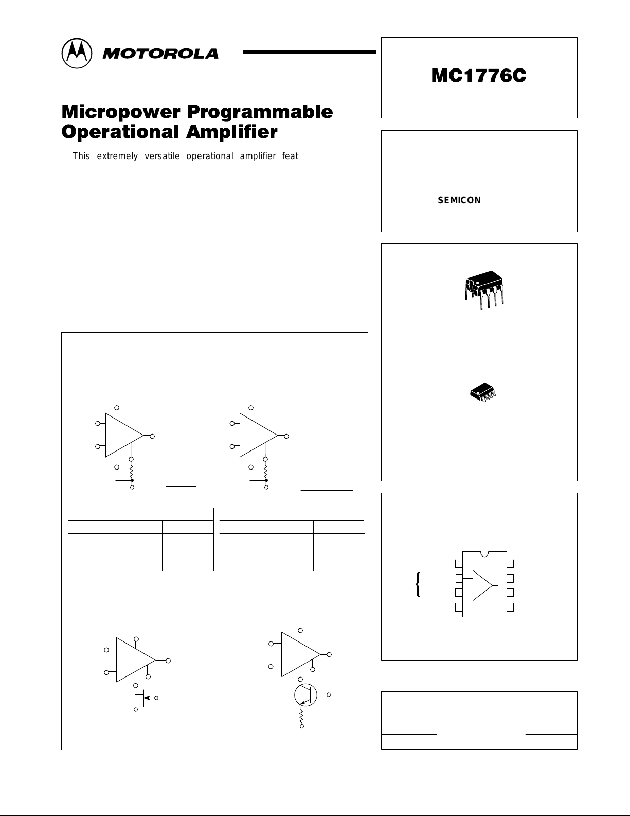
Order this document by MC1776C/D
This extremely versatile operational amplifier features low power
consumption and high input impedance. In addition, the quiescent currents
within the device may be programmed by the choice of an external resistor
value or current source applied to the I
input. This allows the amplifier’s
set
characteristics to be optimized for input current and power consumption
despite wide variations in operating power supply voltages.
• ±1.2 V to ±18 V Operation
• Wide Programming Range
• Offset Null Capability
• No Frequency Compensation Required
• Low Input Bias Currents
• Short Circuit Protection
Resistive Programming
(See Figure 1)
R
to Ground R
set
V
7
CC
2
–
3
+
4
Typical R
VCC, VEEI
±6.0 V
±10 V
±12 V
±15 V
V
EE
set
6
8
R
set
VCC – 0.6
I
=
set
Values
set
= 1.5 µAI
3.6 MΩ
6.2 MΩ
7.5 MΩ
10 MΩ
R
set
= 15 µA
set
360 kΩ
620 kΩ
750 kΩ
1.0 MΩ
VCC, VEEI
Active Programming
FET Current Source Bipolar Current Source
to Negative Supply
set
(Recommended for supply voltage
less than ±6.0 V)
V
7
CC
2
–
3
+
4
±1.5 V
±3.0 V
±6.0 V
±15 V
V
EE
6
8
R
set
I
set
Typical R
= 1.5 µAI
set
1.6 MΩ
3.6 MΩ
7.5 MΩ
20 MΩ
VCC – 0.6 – V
=
Values
set
R
set
set
= 15 µA
160 kΩ
360 kΩ
750 kΩ
2.0 MΩ
EE
PROGRAMMABLE
OPERATIONAL AMPLIFIER
SEMICONDUCTOR
TECHNICAL DATA
8
1
P1 SUFFIX
PLASTIC PACKAGE
CASE 626
8
1
D SUFFIX
PLASTIC PACKAGE
CASE 751
(SO–8)
PIN CONNECTIONS
Input
Offset Null
Invert
Noninvert
V
EE
1
2
–
+
3
4
8
I
set
7
V
CC
6
Output
5
Offset Null
7
V
2
3
Pins not shown are not connected.
CC
–
+
8
V
EE
6
4
V
EE
V
G
MOTOROLA ANALOG IC DEVICE DATA
7
2
–
3
+
8
R
6
4
V
EE
Q
V
B
V
EE
MC1776CD
MC1776CP1
Motorola, Inc. 1996 Rev 5
ORDERING INFORMATION
Device
(Top View)
Operating
Temperature Range
TA = 0° to +70°C
Package
SO–8
Plastic DIP
1
Page 2
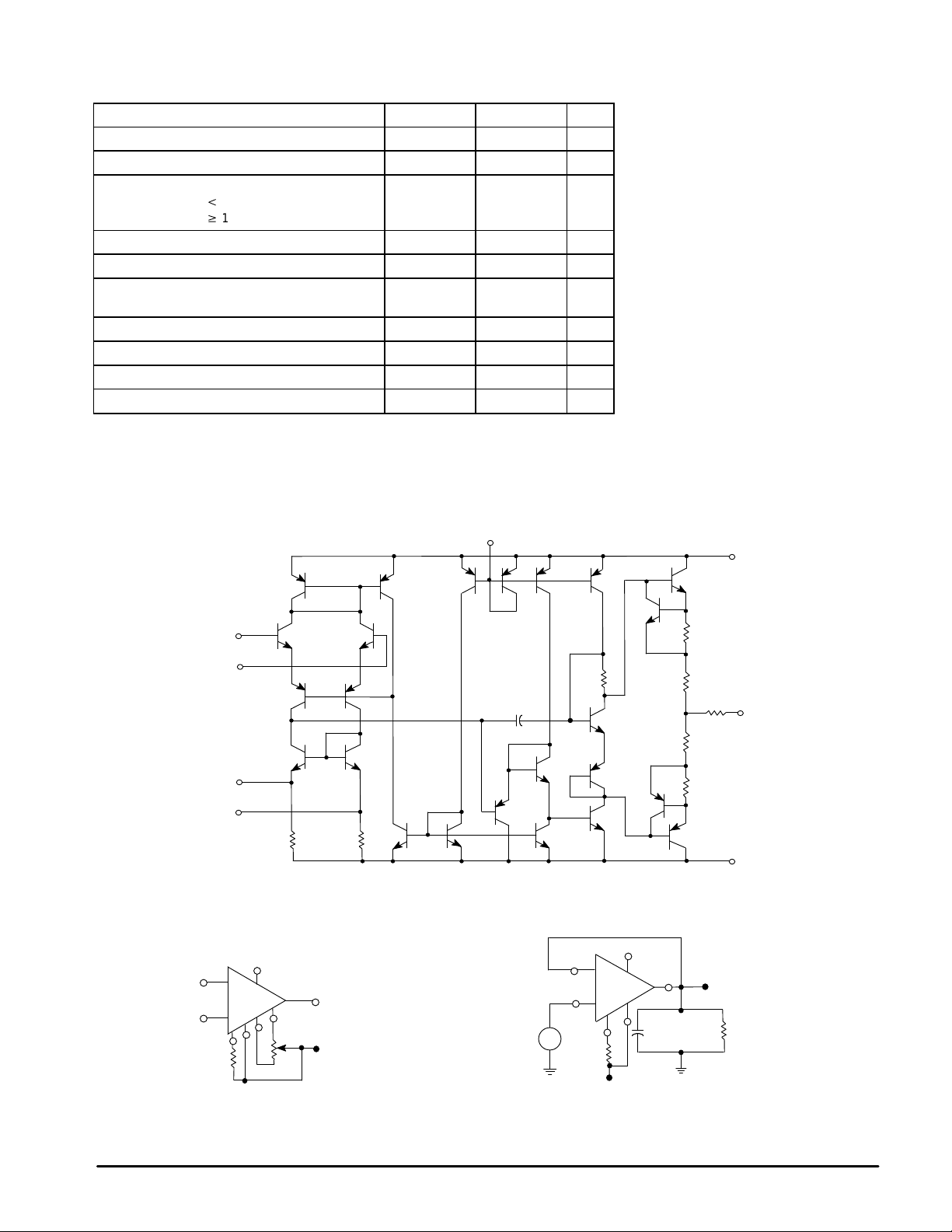
MC1776C
MAXIMUM RATINGS (T
Power Supply Voltages V
Differential Input Voltage V
Common Mode Input Voltage V
VCC and |VEE| t 15 V V
VCC and |VEE| w 15 V ±15
Offset Null to VEE Voltage V
Programming Current I
Programming Voltage V
(Voltage from I
Output Short Circuit Duration (Note 1) t
Operating Temperature Range T
Storage Temperature Range T
Junction Temperature T
NOTE 1. May be to ground or either supply voltage. Rating applies up to a case temperature of +125°C
or ambient temperature of +70°C and I
set
= +25°C, unless otherwise noted.)
A
Rating Symbol Value Unit
CC,VEE
ID
ICM
off–VEE
set
T erminal to Ground) to V
≤ 30 µA.
set
set
SC
A
stg
J
±18 Vdc
±30 Vdc
Vdc
CC,VEE
±0.5 Vdc
500 µA
(VCC –2.0 V) Vdc
CC
Indefinite sec
0 to +70 °C
–65 to +150 °C
150 °C
Representative Schematic Diagram
8
I
set
7
V
CC
2
Inputs
3
1
Offset Null
5
–
+
30 pF
10 k
10 k
2.0 k
100
100
50
50
100
4
V
6
Output
EE
V oltage Offset Null Circuit Transient Response Test Circuit
7
V
7
V
2
3
8
R
set
CC
–
+
1
4
5
100 k
6
V
EE
2
3
V
8
in
R
set
CC
–
+
4
V
EE
6
C
L
V
O
R
L
Pins not shown are
not connected.
2
MOTOROLA ANALOG IC DEVICE DATA
Page 3
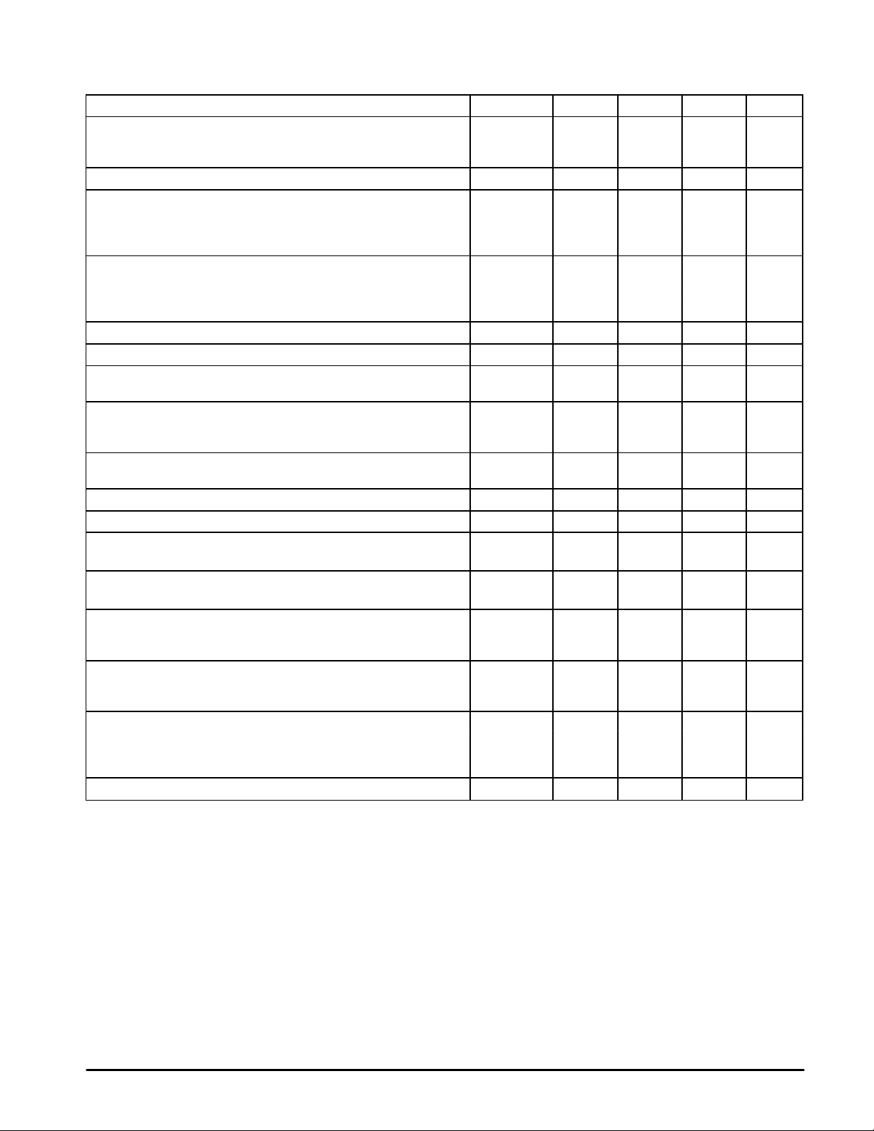
MC1776C
ELECTRICAL CHARACTERISTICS (V
Characteristic Symbol Min Typ Max Unit
Input Offset Voltage (RS ≤ 10 kΩ) V
TA = +25°C – 2.0 6.0
T
* ≤ TA ≤ T
low
Offset Voltage Adjustment Range V
Input Offset Current I
TA = +25°C – 0.7 6.0
TA = T
high
TA = T
low
Input Bias Current I
TA = +25°C – 2.0 10
TA = T
high
TA = T
low
Input Resistance r
Input Capacitance c
Input Voltage Range V
T
≤ TA ≤ T
low
Large Signal Voltage Gain A
RL ≥ 75 kΩ, VO = ±1.0 V , TA = +25°C 25 k 200 k –
RL ≥ 75 kΩ, VO = ±1.0 V , T
Output Voltage Swing V
RL ≥ 75 kΩ, T
Output Resistance r
Output Short Circuit Current I
Common Mode Rejection CMR dB
RS ≤ 10 kΩ, T
Supply Voltage Rejection Ratio PSRR µV/V
RS ≤ 10 kΩ, T
Supply Current ICC, I
TA = +25°C – 13 20
T
≤ TA ≤ T
low
Power Dissipation P
TA = +25°C – 78 120
T
≤ TA ≤ T
low
Transient Response (Unity Gain)
Vin = 20 mV, RL ≥ 5.0 kΩ, CL = 100 pF
Rise Time t
Overshoot os – 0 – %
Slew Rate (RL ≥ 5.0 kΩ) S
*T
= 0°CT
low
* – – 7.5
high
high
≤ TA ≤ T
low
≤ TA ≤ T
low
low
low
high
high
high
≤ TA ≤ T
≤ TA ≤ T
= +70°C
high
high
high
= +3.0 V, VEE = –3.0 V, I
CC
high
= 1.5 µA, TA = +25°C, unless otherwise noted.*)
set
IO
IOR
IO
IB
i
i
ID
VOL
O
o
SC
EE
D
TLH
R
– 9.0 – mV
– – 6.0
– – 10
– – 10
– – 20
– 50 – MΩ
– 2.0 – pF
+1.0 – –
25 k – –
±2.0 ±2.4 –
– 5.0 – kΩ
– 3.0 – mA
70 86 –
– 25 200
– – 25
– – 150
– 3.0 – µs
– 0.03 – V/µs
mV
nA
nA
V
V/V
V
µA
µW
MOTOROLA ANALOG IC DEVICE DATA
3
Page 4
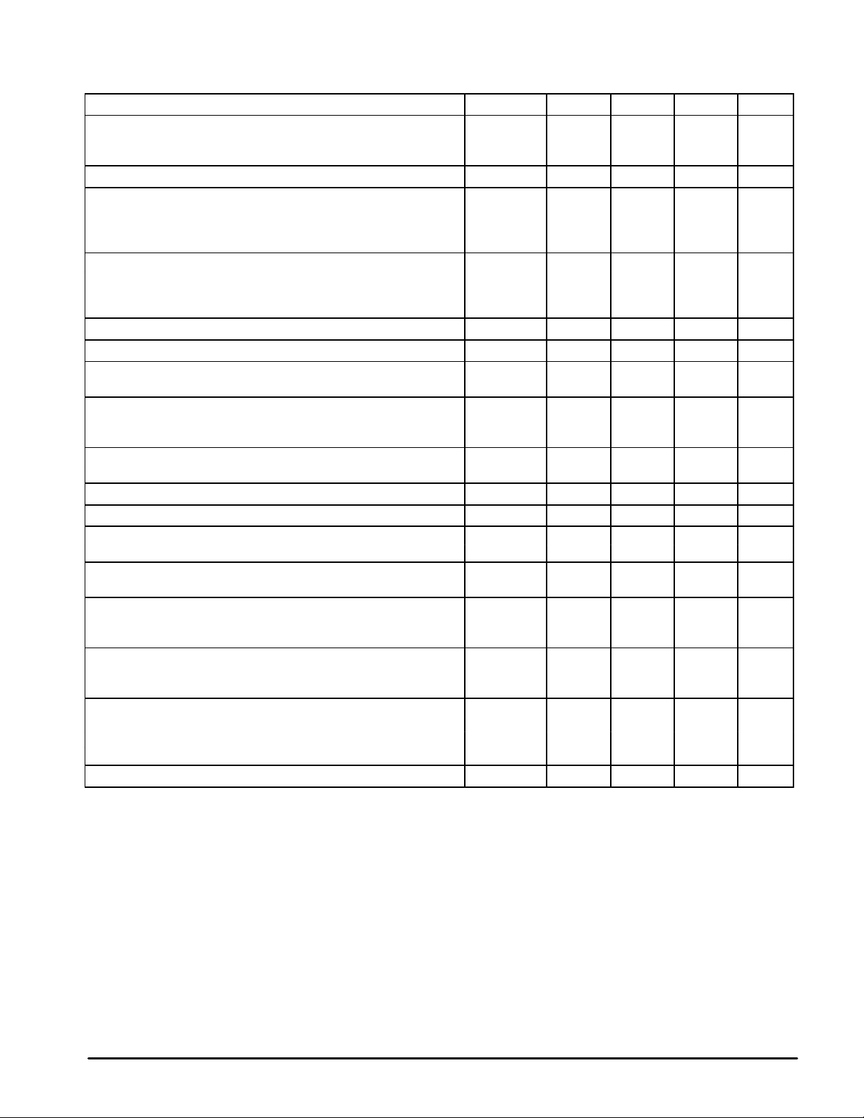
MC1776C
ELECTRICAL CHARACTERISTICS (V
Characteristic Symbol Min Typ Max Unit
Input Offset Voltage (RS ≤ 10 kΩ) V
TA = +25°C – 2.0 6.0
T
* ≤ TA ≤ T
low
Offset Voltage Adjustment Range V
Input Offset Current I
TA = +25°C – 2.0 25
TA = T
high
TA = T
low
Input Bias Current I
TA = +25°C – 15 50
TA = T
high
TA = T
low
Input Resistance r
Input Capacitance c
Input Voltage Range V
T
≤ TA ≤ T
low
Large Signal Voltage Gain A
RL ≥ 5.0 kΩ, VO = ±1.0 V , TA = +25°C 25 k 200 k –
RL ≥ 5.0 kΩ, VO = ±1.0 V , T
Output Voltage Swing V
RL ≥ 5.0 kΩ, T
Output Resistance r
Output Short Circuit Current I
Common Mode Rejection CMR dB
RS ≤ 10 kΩ, T
Supply Voltage Rejection Ratio PSRR µV/V
RS ≤ 10 kΩ, T
Supply Current ICC, I
TA = +25°C – 130 170
T
≤ TA ≤ T
low
Power Dissipation P
TA = +25°C – 780 1020
T
≤ TA ≤ T
low
Transient Response (Unity Gain)
Vin = 20 mV, RL ≥ 5.0 kΩ, CL = 100 pF
Rise Time t
Overshoot os – 5.0 – %
Slew Rate (RL ≥ 5.0 kΩ) S
*T
= 0°CT
low
* – – 7.5
high
high
≤ TA ≤ T
low
≤ TA ≤ T
high
high
high
low
≤ TA ≤ T
low
≤ TA ≤ T
low
= +70°C
high
high
high
= +3.0 V, VEE = –3.0 V, I
CC
high
= 15 µA, TA = +25°C, unless otherwise noted.*)
set
IO
IOR
IO
IB
i
i
ID
VOL
O
o
SC
EE
D
TLH
R
– 18 – mV
– – 25
– – 40
– – 50
– – 100
– 5.0 – MΩ
– 2.0 – pF
±1.0 – –
25 k – –
±2.0 ±2.1 –
– 1.0 – kΩ
– 5.0 – mA
70 86 –
– 25 200
– – 180
– – 1080
– 0.6 – µs
– 0.35 – V/µs
mV
nA
nA
V
V/V
V
µA
µW
4
MOTOROLA ANALOG IC DEVICE DATA
Page 5

MC1776C
ELECTRICAL CHARACTERISTICS (V
Characteristic Symbol Min Typ Max Unit
Input Offset Voltage (RS ≤ 10 kΩ) V
TA = +25°C – 2.0 6.0
T
* ≤ TA ≤ T
low
Offset Voltage Adjustment Range V
Input Offset Current I
TA = +25°C – 0.7 6.0
TA = T
high
TA = T
low
Input Bias Current I
TA = +25°C – 2.0 10
TA = T
high
TA = T
low
Input Resistance r
Input Capacitance c
Input Voltage Range V
T
≤ TA ≤ T
low
Large Signal Voltage Gain A
RL ≥ 75 kΩ, VO = ±10 V, TA = +25°C 50 k 400 k –
RL ≥ 75 kΩ, VO = ±10 V, T
Output Voltage Swing V
RL ≥ 75 kΩ, TA = +25°C ±12 ±14 –
RL ≥ 75 kΩ, T
Output Resistance r
Output Short Circuit Current I
Common Mode Rejection CMR dB
RS ≤ 10 kΩ, T
Supply Voltage Rejection Ratio PSRR µV/V
RS ≤ 10 kΩ, T
Supply Current ICC, I
TA = +25°C – 20 30
T
≤ TA ≤ T
low
Power Dissipation P
TA = +25°C – 780 0.9
T
≤ TA ≤ T
low
Transient Response (Unity Gain)
Vin = 20 mV, RL ≥ 5.0 kΩ, CL = 100 pF
Rise Time t
Overshoot os – 0 – %
Slew Rate (RL ≥ 5.0 kΩ) S
*T
= 0°CT
low
* – – 7.5
high
high
≤ TA ≤ T
low
≤ TA ≤ T
low
high
high
high
low
low
= +70°C
≤ TA ≤ T
≤ TA ≤ T
high
high
high
= +15 V, VEE = –15 V, I
CC
high
= 1.5 µA, TA = +25°C, unless otherwise noted.*)
set
IO
IOR
IO
IB
i
i
ID
VOL
O
o
SC
EE
D
TLH
R
– 9.0 – mV
– – 6.0
– – 10
– – 10
– – 20
– 50 – MΩ
– 2.0 – pF
±10 – –
50 k – –
±10 – –
– 5.0 – kΩ
– 3.0 – mA
70 90 –
– 25 200
– – 35
– – 1.05
– 1.6 – µs
– 0.1 – V/µs
mV
nA
nA
V
V/V
V
µA
mW
MOTOROLA ANALOG IC DEVICE DATA
5
Page 6

MC1776C
ELECTRICAL CHARACTERISTICS (V
Characteristic Symbol Min Typ Max Unit
Input Offset Voltage (RS ≤ 10 kΩ) V
TA = +25°C – 2.0 6.0
T
* ≤ TA ≤ T
low
Offset Voltage Adjustment Range V
Input Offset Current I
TA = +25°C – 2.0 25
TA = T
high
TA = T
low
Input Bias Current I
TA = +25°C – 15 50
TA = T
high
TA = T
low
Input Resistance r
Input Capacitance c
Input Voltage Range V
T
≤ TA ≤ T
low
Large Signal Voltage Gain A
RL ≥ 5.0 kΩ, VO = ±10 V, TA = +25°C 50 k 400 k –
RL ≥ 75 kΩ, VO = ±10 V, T
Output Voltage Swing V
RL ≥ 5.0 kΩ, TA = +25°C ±10 ±13 –
RL ≥ 75 kΩ, T
Output Resistance r
Output Short Circuit Current I
Common Mode Rejection CMR dB
RS ≤ 10 kΩ, T
Supply Voltage Rejection Ratio PSRR µV/V
RS ≤ 10 kΩ, T
Supply Current ICC, I
TA = +25°C – 160 190
T
≤ TA ≤ T
low
Power Dissipation P
TA = +25°C – – 5.7
T
≤ TA ≤ T
low
Transient Response (Unity Gain)
Vin = 20 mV, RL ≥ 5.0 kΩ, CL = 100 pF
Rise Time t
Overshoot os – 10 – %
Slew Rate (RL ≥ 5.0 kΩ) S
*T
= 0°CT
low
* – – 7.5
high
high
≤ TA ≤ T
low
≤ TA ≤ T
low
high
high
high
low
low
= +70°C
≤ TA ≤ T
≤ TA ≤ T
high
high
high
= +15 V, VEE = –15 V, I
CC
high
= 15 µA, TA = +25°C, unless otherwise noted.*)
set
IO
IOR
IO
IB
i
i
ID
VOL
O
o
SC
EE
D
TLH
R
– 18 – mV
– – 25
– – 40
– – 50
– – 100
– 5.0 – MΩ
– 2.0 – pF
±10 – –
50 k – –
±10 – –
– 1.0 – kΩ
– 12 – mA
70 90 –
– 25 200
– – 200
– – 6.0
– 0.35 – µs
– 0.8 – V/µs
mV
nA
nA
V
V/V
V
µA
µW
6
MOTOROLA ANALOG IC DEVICE DATA
Page 7

100 M
)
Ω
1.0 M
, SET RESISTOR (R
set
100 k
10 M
Figure 1. Set Current versus Set Resistor
VCC = +15 V
VEE = –15 V
R
to V
set
EE
VCC = +15 V
VCC = +3.0 V
VEE = –3.0 V
R
to V
set
EE
VCC = +3.0 V
VEE = –3.0 V
R
to GND
set
VEE = –15 V
R
set
MC1776C
to GND
µ
( A)
Figure 2. Positive Standby Supply Current
versus Set Current
1000
+3.0 V ≤ VCC ≤ +18 V
≥
VEE ≥ –18 V
–3.0 V
100
10
1.0
10 k
0.1 1.0 10 100
I
, SET CURRENT (µA)
set
Figure 3. Open Loop Gain versus Set Current Figure 4. Input Bias Current versus Set Current
7
10
VCC = +15 V
RL = 75 k
6
10
5
10
, OPEN LOOP GAIN (V/M)
VOL
A
4
10
0.1 1.0 10 100
I
set
VEE = –15 V
VCC = +3.0 V
VEE = –3.0 V
, SET CURRENT (µA)
0.1
POSITIVE STANDBY SUPPLY CURRENT
0.01 0.1 1.0 10 100
I
, SET CURRENT (µA)
set
100
10
1.0
, INPUT BIAS CURRENT (nA)I
IB
0.1
0.01 0.1 1.0 10 100
+3.0 V ≤ VCC ≤ +18 V
≥
VEE ≥ –18 V
–3.0 V
I
, SET CURRENT (µA)
set
Figure 5. Input Bias Current
versus Ambient T emperature
30
24
18
12
, INPUT BIAS CURRENT (nA)I
6.0
IB
0
–60 –40 –20 0 20 40 60 80 100 120 140
I
set
+3.0 V ≤ VCC ≤ +18 V
–3.0 V
= 1.5 µA
T, TEMPERATURE (°C)
≥
VEE ≥ –18 V
I
set
= 1.5 µA
MOTOROLA ANALOG IC DEVICE DATA
Figure 6. Gain Bandwidth Product
versus Set Current
10 M
1.0 M
VCC = +15 V
VEE = –15 V
100 k
10 k
GBW, GAIN BANDWIDTH PRODUCT (Hz)
1.0 k
0.1 1.0 10 100
I
, SET CURRENT (µA)
set
VCC = +3.0 V
VEE = –3.0 V
7
Page 8

MC1776C
Figure 7. Output Voltage Swing
versus Load Resistance
30
VCC = +15 V
VEE = –15 V
µ
set
= 15
A
RL, LOAD RESISTANCE (Ω)
VCC = +15 V
VEE = –15 V
µ
= 1.5
A
VCC = +3.0 V
VEE = –3.0 V
1.5
I
set
µA ≤
I
24
18
12
, PEAK–TO–PEAK OUTPUT
VOLTAGE SWING (V)
O(pp)
6.0
V
0
1.0 k 10 k 100 k 1.0 M
Figure 9. Output Voltage Swing
versus Supply V oltage
40
36
32
28
24
20
16
12
,OUTPUT VOLTAGE SWING (V)
8.0
O
V
4.0
0
0 2.0 4.0 6.0 8.0 10 12 14 16 18 20
1.5 µA ≤ I
RL = 75 k
VCC, (VEE), SUPPLY VOLTAGES (V)
≤ 15 mA
set
I
= 1.5 µA
set
RL = 5.0 k
I
≤ 15 µA
set
I
= 15 µA
set
RL = 5.0 k
Figure 8. Supply Current
versus Ambient T emperature
150
120
µ
( A)I
I
= 1.5 µA
set
90
VCC = +15 V
VEE = –15 V
60
, SUPPLY CURRENT
30
S
0
I
= 1.5 µA
set
VCC = +15 V
VEE = –15 V
–60 –40 –20 0 20 40 60 80 100 120 140
T, AMBIENT TEMPERATURE (
I
= 1.5 µA
set
VCC = +3.0 V
VEE = –3.0 V
I
= 15 µA
set
VCC = +3.0 V
VEE = –3.0 V
°
C)
Figure 10. Slew Rate
versus Set Current
10
1.0
µ
(V s)
0.1
SR, SLEW RATE
0.01
0.001
0.01 0.1 1.0 10 100
VCC = +15 V
VEE = –15 V
VCC = +3.0 V
VEE = –3.0 V
I
, SET CURRENT (µA)
set
2
Figure 11. Input Noise Voltage
versus Set Current
–13
10
–14
10
f = 1.0 kHz
∆
–15
10
–16
10
–17
V(RMS), MEAN SQUARE VOLTAGE(V /Hz)
10
0.01 0.1 1.0 10 100
1 = Hz
≤
VCC ≤ +18 V
+3.0 V
≥
VEE ≥ –18 V
–3.0 V
I
, SET CURRENT (
set
µ
A)
8
Figure 12. Optimum Source Resistance for
Minimum Noise versus Set Current
100
Ω
10
1.0
OPTIMUM SOURCE RESISTANCE (M )
0.1
0.01 0.1 1.0 10 100
I
, SET CURRENT (µA)
set
MOTOROLA ANALOG IC DEVICE DATA
Page 9

MC1776C
Figure 13. Wien Bridge Oscillator
22 k
200 k
10 k
3
C
fo =
2
–
MC1776C
+
4
–15 V
R
1
π
RC
2
Ω
R= 16 k
C = 0.01 µF
+15 V
7
8
R
set
R
(for fo = 1.0 kHz)
6
C
Figure 14. Multiple Feedback Bandpass Filter
V
R
R
V
in
C
1
R
2
5
C
2
3
CC
7
–
MC1776C
+
8
4
R
set
Figure 15. Multiple Feedback Bandpass Filter
(1.0 kHz)
2
3
µ
–
MC1776C
+
4
F
+15 V
7
6
Output
8
2.0 M
–15 V
C
R
Input
V
O
1
R
2
for a 1.0 kHz filter
with Q = 10
and A (fo) = 1
C
R
5
R1 = 160 k
R2 = 820
R5 = 300 k
C = 0.01
Figure 16. Gated Amplifier
1 M
10 k
Input
10 k
6
V
O
10 k
Gate
2
3
5.6 k
+15 V
7
–
MC1776C
+
4
8
270 k
Q
–15 V
2.7 M
6
Output
V
CC
15 V
V
EE
For a given:
fo = center frequency
A (fo) = Gain at center frequency
Q = quality factor
To obtain less than 10% error from the operational amplifier:
QO f
o
≤
0.1
where fo and GBW are expressed in Hz. GBW is available from
Figure 6 as a function of Set Current, I
GBW
Choose a value for C, then
Q
R5 =
π
foC
R5
R1 =
2A (fo)
R1,R5
R2 =
4Q2 R1–R5
.
set
MOTOROLA ANALOG IC DEVICE DATA
Figure 17. High Input Impedance Amplifier
10 k
90 k
6
OutputInput
500 k
500 k
50 M
2
3
–
MC1776C
+
8
30 M
50 M
+15 V
7
4
–15 V
9
Page 10

MC1776C
OUTLINE DIMENSIONS
P1 SUFFIX
PLASTIC PACKAGE
CASE 626–05
ISSUE K
58
NOTE 2
–T–
SEATING
PLANE
H
14
F
–A–
N
D
G
0.13 (0.005) B
A
E
B
D
58
1
4
e
C
A1
B
–B–
C
K
M
A
T
0.25MB
H
A
SS
A0.25MCB
L
J
M
M
M
PLASTIC PACKAGE
M
h
SEATING
PLANE
0.10
D SUFFIX
CASE 751–05
(SO–8)
ISSUE R
X 45
_
q
NOTES:
1. DIMENSION L TO CENTER OF LEAD WHEN
FORMED PARALLEL.
2. PACKAGE CONTOUR OPTIONAL (ROUND OR
SQUARE CORNERS).
3. DIMENSIONING AND TOLERANCING PER ANSI
Y14.5M, 1982.
DIM MIN MAX MIN MAX
A 9.40 10.16 0.370 0.400
B 6.10 6.60 0.240 0.260
C 3.94 4.45 0.155 0.175
D 0.38 0.51 0.015 0.020
F 1.02 1.78 0.040 0.070
G 2.54 BSC 0.100 BSC
H 0.76 1.27 0.030 0.050
J 0.20 0.30 0.008 0.012
K 2.92 3.43 0.115 0.135
L 7.62 BSC 0.300 BSC
M ––– 10 ––– 10
N 0.76 1.01 0.030 0.040
NOTES:
C
L
1. DIMENSIONING AND TOLERANCING PER ASME
Y14.5M, 1994.
2. DIMENSIONS ARE IN MILLIMETERS.
3. DIMENSION D AND E DO NOT INCLUDE MOLD
PROTRUSION.
4. MAXIMUM MOLD PROTRUSION 0.15 PER SIDE.
5. DIMENSION B DOES NOT INCLUDE MOLD
PROTRUSION. ALLOWABLE DAMBAR
PROTRUSION SHALL BE 0.127 TOTAL IN EXCESS
OF THE B DIMENSION AT MAXIMUM MATERIAL
CONDITION.
MILLIMETERS
DIM MIN MAX
A 1.35 1.75
A1 0.10 0.25
B 0.35 0.49
C 0.18 0.25
D 4.80 5.00
E
H 5.80 6.20
h
L 0.40 1.25
q
INCHESMILLIMETERS
__
3.80 4.00
1.27 BSCe
0.25 0.50
0 7
__
10
MOTOROLA ANALOG IC DEVICE DATA
Page 11

MC1776C
Motorola reserves the right to make changes without further notice to any products herein. Motorola makes no warranty , representation or guarantee regarding
the suitability of its products for any particular purpose, nor does Motorola assume any liability arising out of the application or use of any product or circuit, and
specifically disclaims any and all liability, including without limitation consequential or incidental damages. “T ypical” parameters which may be provided in Motorola
data sheets and/or specifications can and do vary in different applications and actual performance may vary over time. All operating parameters, including “Typicals”
must be validated for each customer application by customer’s technical experts. Motorola does not convey any license under its patent rights nor the rights of
others. Motorola products are not designed, intended, or authorized for use as components in systems intended for surgical implant into the body, or other
applications intended to support or sustain life, or for any other application in which the failure of the Motorola product could create a situation where personal injury
or death may occur. Should Buyer purchase or use Motorola products for any such unintended or unauthorized application, Buyer shall indemnify and hold Motorola
and its officers, employees, subsidiaries, affiliates, and distributors harmless against all claims, costs, damages, and expenses, and reasonable attorney fees
arising out of, directly or indirectly, any claim of personal injury or death associated with such unintended or unauthorized use, even if such claim alleges that
Motorola was negligent regarding the design or manufacture of the part. Motorola and are registered trademarks of Motorola, Inc. Motorola, Inc. is an Equal
Opportunity/Affirmative Action Employer.
MOTOROLA ANALOG IC DEVICE DATA
11
Page 12

MC1776C
How to reach us:
USA/EUROPE/Locations Not Listed: Motorola Literature Distribution; JAPAN: Nippon Motorola Ltd.; Tatsumi–SPD–JLDC, 6F Seibu–Butsuryu–Center,
P.O. Box 20912; Phoenix, Arizona 85036. 1–800–441–2447 or 602–303–5454 3–14–2 T atsumi Koto–Ku, Tokyo 135, Japan. 03–81–3521–8315
MFAX: RMF AX0@email.sps.mot.com – TOUCHT ONE 602–244–6609 ASIA/PACIFIC: Motorola Semiconductors H.K. Ltd.; 8B Tai Ping Industrial Park,
INTERNET: http://Design–NET.com 51 Ting Kok Road, Tai Po, N.T., Hong Kong. 852–26629298
12
◊
MOTOROLA ANALOG IC DEVICE DATA
MC1776C/D
*MC1776C/D*
 Loading...