

Page 1
SEMICONDUCTOR TECHNICAL DATA
1
REV 2
Motorola, Inc. 1997
1/97
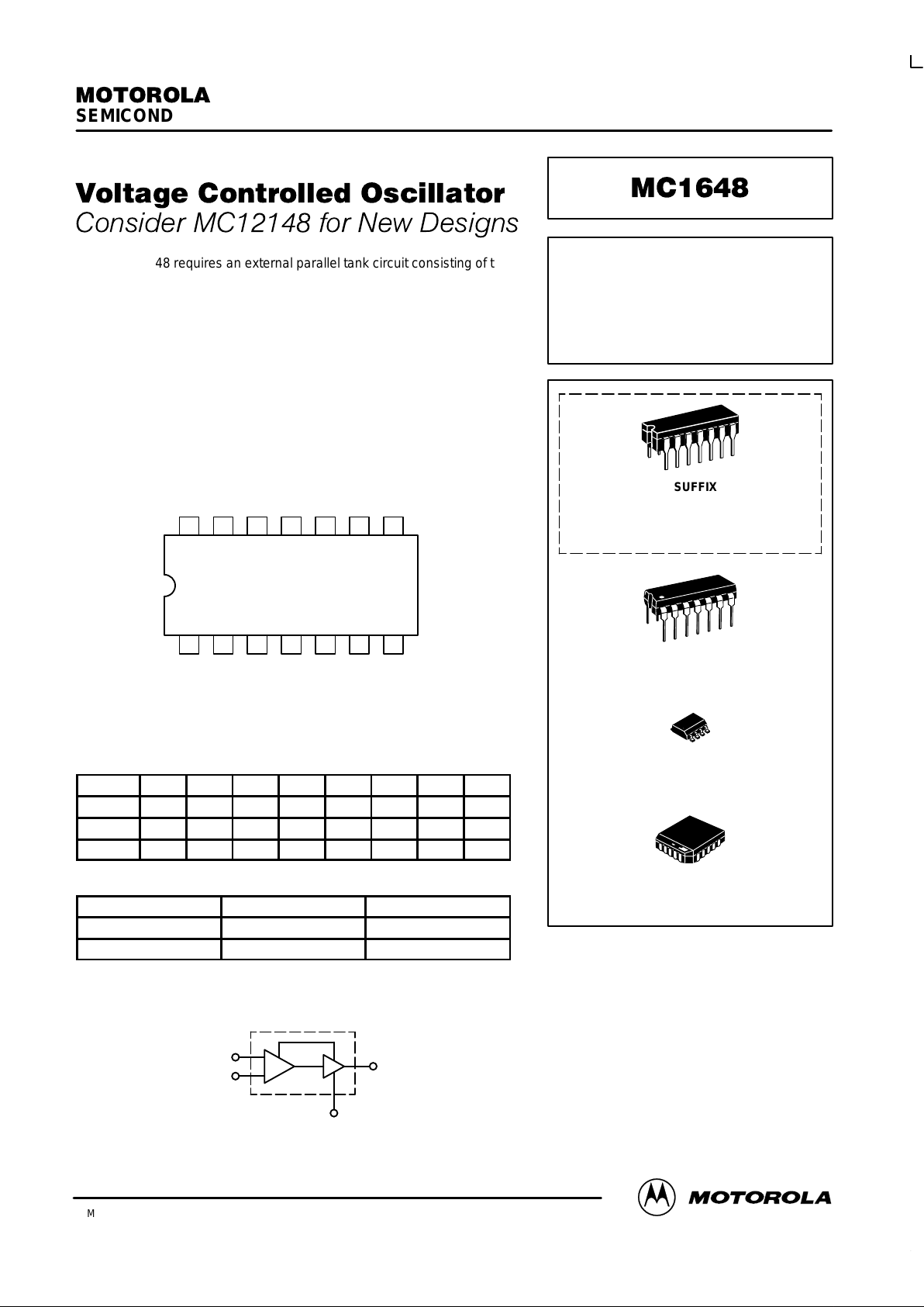
The MC1648 requires an external parallel tank circuit consisting of the
inductor (L) and capacitor (C). For Maximum Performance QL ≥ 100 at
Frequency of Operation.
A varactor diode may be incorporated into the tank circuit to provide a
voltage variable input for the oscillator (VCO). The MC1648 was
designed for use in the Motorola Phase–Locked Loop shown in Figure 9.
This device may also be used in many other applications requiring a fixed
or variable frequency clock source of high spectral purity. (See Figure 2)
The MC1648 may be operated from a +5.0Vdc supply or a –5.2Vdc
supply, depending upon system requirements.
NOTE: The MC1648 is NOT useable as a crystal oscillator.
Pinout: 14–Lead Package (Top View)
1314 12 11 10 9 8
21 34567
VCCNC TANK NC BIAS NC V
EE
VCCNC OUT NC AGC NC V
EE
Pin assignment is for Dual–in–Line Package.
For PLCC pin assignment, see the MC1648 Non–Standard Pin Conversion T able below.
MC1648 NON–STANDARD PIN CONVERSION DATA
Package TANK V
CCVCC
OUT AGC V
EEVEE
BIAS
8 D 1 2 3 4 5 6 7 8
14 L,P 12 14 1 3 5 7 8 10
20FN 18 20 2 4 8 10 12 14
*NOTE – All unused pins are not connected.
Supply Voltage
GND Pins Supply Pins
+5.0Vdc 7,8 1,14
–5.2Vdc 1,14 7,8
5
AGC
LOGIC DIAGRAM
3
TANK 12
BIAS POINT 10
OUTPUT
•
Input Capacitance = 6.0pF (TYP)
•
Maximum Series Resistance for L (External Inductance) = 50
Ω
(TYP)
•
Power Dissipation = 150mW (TYP)/Pkg (+5.0Vdc Supply)
•
Maximum Output Frequency = 225MHz (TYP)
V
CC1
= Pin 1
V
CC2
= Pin 14
VEE = Pin 7
VOLTAGE
CONTROLLED
OSCILLATOR
FN SUFFIX
20–LEAD PLCC PACKAGE
CASE 775–02
L SUFFIX
14–LEAD CERAMIC PACKAGE
CASE 632–08
P SUFFIX
14–LEAD PLASTIC PACKAGE
CASE 646–06
D SUFFIX
8–PIN PLASTIC SOIC PACKAGE
CASE 751–05
Not Recommended for New Designs
Page 2

MC1648
MOTOROLA HIPERCOMM
BR1334 — Rev 4
2
Figure 1. Circuit Schematic
5
AGC
8
V
EE
12
TANK
10
BIAS
POINT
7
V
EE1
V
CC2
14
V
CC1
1
Q4
Q3 Q2
Q1
Q5
D1
Q8
Q7 Q6
Q9
Q10Q11
D2
3
OUTPUT
TEST VOLTAGE/CURRENT VALUES
@ Test
(Volts) mAdc
Temperature
V
IHmax
V
ILmin
V
CC
I
L
MC1648
–30°C +2.0 +1.5 +5.0 –5.0
+25°C +1.85 +1.35 +5.0 –5.0
+85°C +1.7 +1.2 +5.0 –5.0
Note: SOIC “D” package guaranteed –30°C to +70°C only
ELECTRICAL CHARACTERISTICS (Supply Voltage = +5.0V)
–30°C +25°C +85°C
Symbol Characteristic Min Max Min Max Min Max Unit Condition
I
E
Power Supply Drain Current – – – 41 – –
mAdc
Inputs and outputs open
V
OH
Logic “1” Output Voltage 3.955 4.185 4.04 4.25 4.11 4.36 Vdc V
ILmin
to Pin 12, IL @ Pin 3
V
OL
Logic “0” Output Voltage 3.16 3.4 3.2 3.43 3.22 3.475 Vdc V
IHmax
to Pin 12, IL @ Pin 3
V
BIAS
1
Bias Voltage 1.6 1.9 1.45 1.75 1.3 1.6 Vdc V
ILmin
to Pin 12
Min Typ Max Min Typ Max Min Typ Max Unit Condition
V
P–P
Peak–to–Peak Tank Voltage – – – – 400 – – – – mV See Figure 3
Vdc Output Duty Cycle – – – – 50 – – – – %
f
max
2
Oscillation Frequency – 225 – 200 225 – – 225 – MHz
1. This measurement guarantees the dc potential at the bias point for purposes of incorporating a varactor tuning diode at this point.
2. Frequency variation over temperature is a direct function of the ∆C/∆ Temperature and ∆L/∆ Temperature.
Page 3
MC1648
HIPERCOMM
BR1334 — Rev 4
3 MOTOROLA
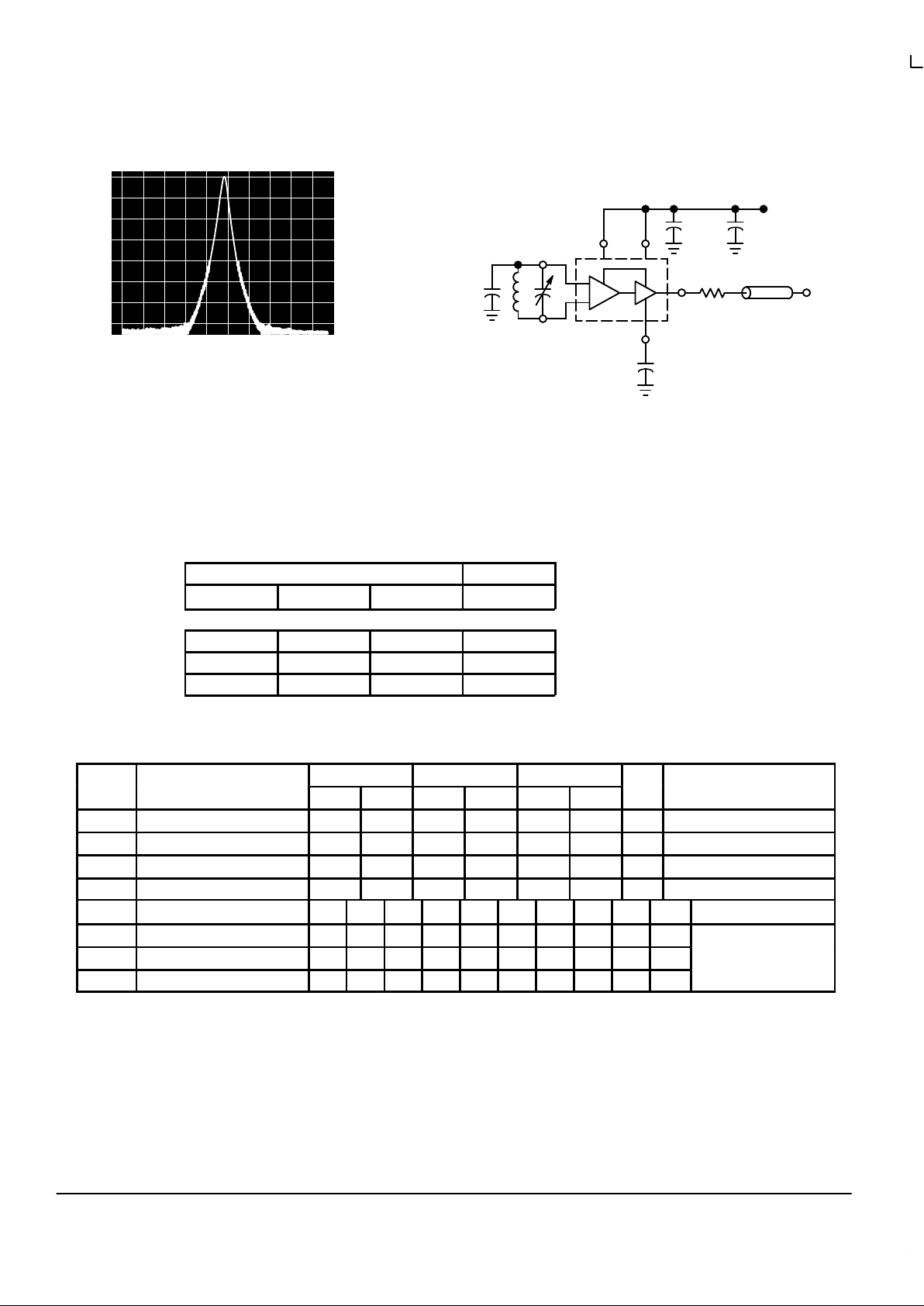
Figure 2. Spectral Purity of Signal Output for 200MHz Testing
B.W. = 10 kHz
Center Frequency = 100 MHz
Scan Width = 50 kHz/div
Vertical Scale = 10 dB/div
0.1µF
1200*
CL
10
12
5
0.1
µ
F
3
SIGNAL
UNDER
TEST
10µF0.1µF
114
L=40nH
C=10pF
+5.0Vdc
L: Micro Metal torroid #T20–22, 8 turns #30 Enameled Copper wire.
C = 3.0–35pF
* The 1200 ohm resistor and the scope termination impedance constitute a 25:1
attenuator probe. Coax shall be CT–075–50 or equivalent.
TEST VOLTAGE/CURRENT VALUES
@ Test
(Volts) mAdc
Temperature
V
IHmax
V
ILmin
V
EE
I
L
MC1648
–30°C –3.2 –3.7 –5.2 –5.0
+25°C –3.35 –3.85 –5.2 –5.0
+85°C –3.5 –4.0 –5.2 –5.0
Note: SOIC “D” package guaranteed –30°C to +70°C only
ELECTRICAL CHARACTERISTICS (Supply Voltage = –5.2V)
–30°C +25°C +85°C
Symbol Characteristic Min Max Min Max Min Max Unit Condition
I
E
Power Supply Drain Current – – – 41 – –
mAdc
Inputs and outputs open
V
OH
Logic “1” Output Voltage –1.045 –0.815 –0.96 –0.75 –0.89 –0.64 Vdc V
ILmin
to Pin 12, IL @ Pin 3
V
OL
Logic “0” Output Voltage –1.89 –1.65 –1.85 –1.62 –1.83 –1.575 Vdc V
IHmax
to Pin 12, IL @ Pin 3
V
BIAS
1
Bias Voltage –3.6 –3.3 –3.75 –3.45 –3.9 –3.6 Vdc V
ILmin
to Pin 12
Min Typ Max Min Typ Max Min Typ Max Unit Condition
V
P–P
Peak–to–Peak Tank Voltage – – – – 400 – – – – mV See Figure 3
Vdc Output Duty Cycle – – – – 50 – – – – %
f
max
2
Oscillation Frequency – 225 – 200 225 – – 225 – MHz
1. This measurement guarantees the dc potential at the bias point for purposes of incorporating a varactor tuning diode at this point.
2. Frequency variation over temperature is a direct function of the ∆C/∆ Temperature and ∆L/∆ Temperature.
Page 4
MC1648
MOTOROLA HIPERCOMM
BR1334 — Rev 4
4
Figure 3. Test Circuit and Waveforms
0.1µF
1200
CL
10
12
0.1µF
3
*
V
CC
**
***
5
V
EE
QL
≥
100
* Use high impedance probe (>1.0 Megohm must be used).
** The 1200 ohm resistor and the scope termination impedance constitute
a 25:1 attenuator probe. Coax shall be CT–070–50 or equivalent.
***Bypass only that supply opposite ground.
50%
t
a
t
b
V
P–P
PRF = 1.0MHz
Duty Cycle (Vdc) –
t
a
t
b
7 8
114
0.1µF 0.1µF
***
OPERA TING CHARACTERISTICS
Figure 1 illustrates the circuit schematic for the MC1648.
The oscillator incorporates positive feedback by coupling the
base of transistor Q6 to the collector of Q7. An automatic gain
control (AGC) is incorporated to limit the current through the
emitter–coupled pair of transistors (Q7 and Q6) and allow
optimum frequency response of the oscillator.
In order to maintain the high Q of the oscillator, and
provide high spectral purity at the output, transistor Q4 is
used to translate the oscillator signal to the output differential
pair Q2 and Q3. Q2 and Q3, in conjunction with output
transistor Q1, provides a highly buffered output which
produces a square wave. Transistors Q9 and Q11 provide
the bias drive for the oscillator and output buffer. Figure 2
indicates the high spectral purity of the oscillator output
(pin 3).
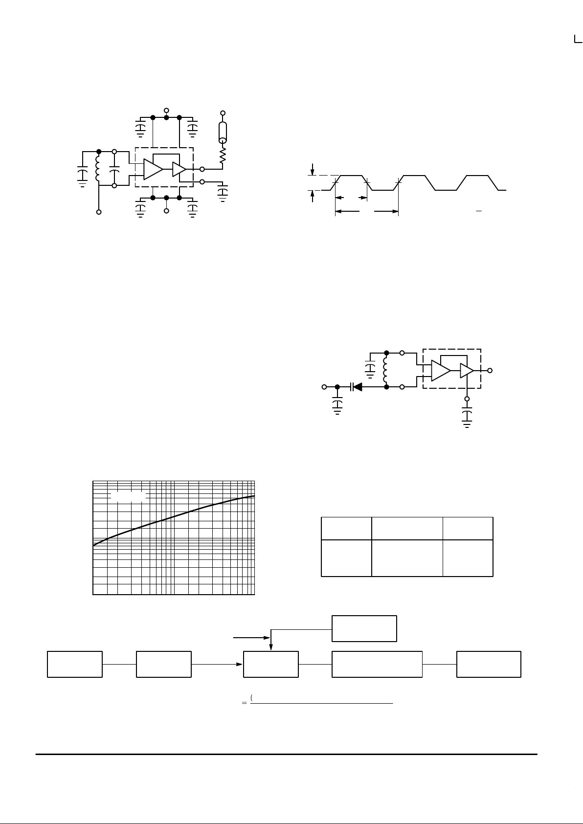
When operating the oscillator in the voltage controlled
mode (Figure 4), it should be noted that the cathode of the
varactor diode (D) should be biased at least “2” VBE above
VEE (≈1.4V for positive supply operation).
When the MC1648 is used with a constant dc voltage to
the varactor diode, the output frequency will vary slightly
because of internal noise. This variation is plotted versus
operating frequency in Figure 5.
Figure 4. The MC1648 Operating in the
Voltage Controlled Mode
0.1µF
L
10
12
C2
3
5
QL
≥
100
Output
V
in
C1
D
1.0–10
10–60
60–100
f
MHz
Figure 5. Noise Deviation Test Circuit and Waveform
100
1
f, OPERATING FREQUENCY (MHz)
VCC = 5 Vdc
f, FREQUENCY DEVIA TION, RMS (Hz)
10
1
10 100
∆
Frequency Deviation
+
(HP5210A output voltage) (Full Scale Frequency)
1.0Volt
MV2115
MV2115
MV2106
D
100
2.3
0.15
L
µH
Oscillator Tank Components
(Circuit of Figure 4)
BW=1.0kHz Frequency
Meter HP5210A or Equiv
Voltmeter RMS
HP3400A or Equiv
MC1648
Frequency (f)
MC1648
Under Test
Attenuator
Product
Detector
Signal Generator
HP608 or Equiv
10mV 20kHz
300mV
20kHz above MC1648 Frequency
Page 5

MC1648
HIPERCOMM
BR1334 — Rev 4
5 MOTOROLA
* The 1200 ohm resistor and the scope termination impedance consti-
tute a 25:1 attenuator probe. Coax shall be CT–070–50 or equivalent.
NOT used in normal operation.
** Input resistor and cap are for test only. They are NOT necessary for
normal operation.
* The 1200 ohm resistor and the scope termination impedance consti-
tute a 25:1 attenuator probe. Coax shall be CT–070–50 or equivalent.
NOT used in normal operation.
** Input resistor and cap are for test only. They are NOT necessary for
normal operation.
Figure 6
Figure 7
Figure 8
Vin, INPUT VOLTAGE (VOLTS)
Vin, INPUT VOLTAGE (VOLTS)
18
0
8
10
190
50
64
0
Vin, INPUT VOLTAGE (VOLTS)
8
10
56
48
40
32
24
16
2468
f
out
, OUTPUT FREQUENCY (MHz)f
out
, OUTPUT FREQUENCY (MHz)f
out
, OUTPUT FREQUENCY (MHz)
16
14
12
10
24 68
0102468
170
150
130
110
90
70
0.1µF
L
10
12
0.1
µ
F
3
5
V
CC1
= V
CC2
= +5.0Vdc
V
EE1
= V
EE2
= GND
f
out
V
in
MV1401
1200*
5.0µF
L = 0.13
µ
H
QL
≥
100
L: Micro Metal Toroidal Core #T44–10,
4 turns of No. 22 copper wire.
0.1µF
L
10
12
0.1
µ
F
3
5
V
CC1
= V
CC2
= +5.0Vdc
V
EE1
= V
EE2
= GND
f
out
V
in
MV1401
1200*
5.0µF
QL ≥100
C = 500pF
L = 1.58
µ
H
L: Micro Metal Toroidal Core #T44–10,
20 turns of No. 22 copper wire.
C
1.0k
1.0k
* The 1200 ohm resistor and the scope termination impedance consti-
tute a 25:1 attenuator probe. Coax shall be CT–070–50 or equivalent.
NOT used in normal operation.
** Input resistor and cap are for test only. They are NOT necessary for
normal operation.
0.1µF
L
10
12
0.1
µ
F
3
5
V
CC1
= V
CC2
= +5.0Vdc
V
EE1
= V
EE2
= GND
f
out
V
in
1200*
QL ≥100
L = 0.065
µ
H
L: Micro Metal Toroidal Core #T30–12,
6 turns of No. 22 copper wire.
51k
MV1404
5.0µF
**
**
**
**
**
**
Page 6

MC1648
MOTOROLA HIPERCOMM
BR1334 — Rev 4
6
Typical transfer characteristics for the oscillator in the
voltage controlled mode are shown in Figure 6, Figure 7 and
Figure 8. Figure 6 and Figure 8 show transfer characteristics
employing only the capacitance of the varactor diode (plus
the input capacitance of the oscillator, 6.0pF typical).
Figure 7 illustrates the oscillator operating in a voltage
controlled mode with the output frequency range limited. This
is achieved by adding a capacitor in parallel with the tank
circuit as shown. The 1.0kΩ resistor in Figure 6 and Figure 7
is used to protect the varactor diode during testing. It is not
necessary as long as the dc input voltage does not cause the
diode to become forward biased. The larger–valued resistor
(51kΩ) in Figure 8 is required to provide isolation for the
high–impedance junctions of the two varactor diodes.
The tuning range of the oscillator in the voltage controlled
mode may be calculated as:
f
max
f
min
+
CD(max))C
S
Ǹ
CD(min))C
S
Ǹ
where f
min
+
1
2pL(CD(max))CS)
Ǹ
CS = shunt capacitance (input plus external capacitance)
CD = varactor capacitance as a function of bias voltage
Good RF and low–frequency bypassing is necessary on
the power supply pins. (See Figure 2)
Capacitors (C1 and C2 of Figure 4) should be used to
bypass the AGC point and the VCO input (varactor diode),
guaranteeing only dc levels at these points.
For output frequency operation between 1.0MHz and
50MHz a 0.1µF capacitor is sufficient for C1 and C2. At
higher frequencies, smaller values of capacitance should be
used; at lower frequencies, larger values of capacitance. At
high frequencies the value of bypass capacitors depends
directly upon the physical layout of the system. All bypassing
should be as close to the package pins as possible to
minimize unwanted lead inductance.
The peak–to–peak swing of the tank circuit is set internally
by the AGC circuitry. Since voltage swing of the tank circuit
provides the drive for the output buffer, the AGC potential
directly affects the output waveform. If it is desired to have a
sine wave at the output of the MC1648, a series resistor is
tied from the AGC point to the most negative power potential
(ground if +5.0 volt supply is used, –5.2 volts if a negative
supply is used) as shown in Figure 10.
At frequencies above 100 MHz typ, it may be desirable to
increase the tank circuit peak–to–peak voltage in order to
shape the signal at the output of the MC1648. This is
accomplished by tying a series resistor (1.0kΩ minimum)
from the AGC to the most positive power potential (+5.0 volts
if a +5.0 volt supply is used, ground if a –5.2 volt supply is
used). Figure 11 illustrates this principle.
APPLICATIONS INFORMATION
The phase locked loop shown in Figure 9 illustrates the
use of the MC1648 as a voltage controlled oscillator. The
figure illustrates a frequency synthesizer useful in tuners for
FM broadcast, general aviation, maritime and landmobile
communications, amateur and CB receivers. The system
operates from a single +5.0Vdc supply, and requires no
internal translations, since all components are compatible.
Frequency generation of this type offers the advantages of
single crystal operation, simple channel selection, and
elimination of special circuitry to prevent harmonic lockup.
Additional features include dc digital switching (preferable
over RF switching with a multiple crystal system), and a
broad range of tuning (up to 150MHz, the range being set by
the varactor diode).
The output frequency of the synthesizer loop is
determined by the reference frequency and the number
programmed at the programmable counter; f
out
= Nf
ref
. The
channel spacing is equal to frequency (f
ref
).
For additional information on applications and designs for
phase locked–loops and digital frequency synthesizers, see
Motorola Brochure BR504/D, Electronic Tuning Address
Systems, (ETAS).
Figure 10 shows the MC1648 in the variable frequency
mode operating from a +5.0Vdc supply . T o obtain a sine wave
at the output, a resistor is added from the AGC circuit (pin 5)
to VEE.
Figure 11 shows the MC1648 in the variable frequency
mode operating from a +5.0Vdc supply . To extend the useful
range of the device (maintain a square wave output above
175Mhz), a resistor is added to the AGC circuit at pin 5 (1.0
kohm minimum).
Figure 12 shows the MC1648 operating from +5.0Vdc and
+9.0Vdc power supplies. This permits a higher voltage swing
and higher output power than is possible from the MECL
output (pin 3). Plots of output power versus total collector
load resistance at pin 1 are given in Figure 13 and Figure 14
for 100MHz and 10MHz operation. The total collector load
includes R in parallel with Rp of L1 and C1 at resonance. The
optimum value for R at 100MHz is approximately 850 ohms.
Page 7

MC1648
HIPERCOMM
BR1334 — Rev 4
7 MOTOROLA
Figure 9. Typical Frequency Synthesizer Application
Phase
Detector
MC4044
f
ref
Counter Control
Logic
MC12014
MC12012
÷
P, ÷(P+1)
÷
N
p
Programmable
Counter MC4016
÷
A
Programmable
Counter MC4016
Low Pass
Filter
Voltage Controlled
Oscillator
MC1648
Modulus Enable Line
Zero Detect Line
f
out
N = Np
•
P + A
Counter Reset Line
f
out
f
out
= Nf
ref
where
N = Np
•
P + A
Figure 10. Method of Obtaining a Sine–Wave Output Figure 11. Method of Extending the Useful Range
of the MC1648 (Square Wave Output)
10
12
78
3
5
Output
+5.0Vdc
10
12
78
3
5
Output
+5.0Vdc
114
114
1.0k min
Page 8

MC1648
MOTOROLA HIPERCOMM
BR1334 — Rev 4
8
Figure 12. Circuit Used for Collector Output Operation
10
12
0.1
µ
F
3
5
Bias Point
L2* T ank
C2
1.0
µ
F
V
CC2
14 1V
CC1
C1
L1
+5.0V
C3
R
0.01µF
+9.0V
AGC
+5.0V
1.0µF
1.2k
8V
EE2
7V
EE1
* QL ≥ 100
Output
Figure 13. Power Output versus Collector Load Figure 14. Power Output versus Collector Load
TOTAL COLLECT OR LOAD (OHMS)
7
10
TOTAL COLLECT OR LOAD (OHMS)
POWER OUTPUT (mW RMS)
0
10,000
6
5
4
3
2
1
100 1000
POWER OUTPUT (mW RMS)
10 10,000100 1000
14
0
12
10
8
6
4
2
See test circuit, Figure 12, f = 100MHz
C3 = 3.0–35pF
Collector Tank
L1 = 0.22µH C1 = 1.0–7.0pF
R = 50Ω–10kΩ
RP of L1 and C1 = 11kΩ @ 100MHz Resonance
Oscillator Tank
L2 = 4 turns #20 AWG 3/16” ID
C2 = 1.0–7.0pF
See test circuit, Figure 12, f = 10MHz
C3 = 470pF
Collector Tank
L1 = 2.7µH C1 = 24–200pF
R = 50Ω–10kΩ
RP of L1 and C1 = 6.8kΩ @ 10MHz Resonance
Oscillator Tank
L2 = 2.7µH
C2 = 16–150pF
Page 9

MC1648
HIPERCOMM
BR1334 — Rev 4
9 MOTOROLA
OUTLINE DIMENSIONS
P SUFFIX
PLASTIC PACKAGE
CASE 646–06
ISSUE L
18.16
6.10
3.69
0.38
1.02
1.32
0.20
2.92
0°
0.39
19.56
6.60
4.69
0.53
1.78
2.41
0.38
3.43
10
°
1.01
2.54 BSC
7.62 BSC
0.715
0.240
0.145
0.015
0.040
0.052
0.008
0.115
0
°
0.015
SEATING
PLANE
0.100 BSC
0.300 BSC
MIN MINMAX MAX
INCHES MILLIMETERS
DIM
0.770
0.260
0.185
0.021
0.070
0.095
0.015
0.135
10
°
0.039
A
B
C
D
F
G
H
J
K
L
M
N
NOTES:
1. LEADS WITHIN 0.13 (0.005) RADIUS OF TRUE
POSITION AT SEATING PLANE AT MAXIMUM
MATERIAL CONDITION.
2. DIMENSION L TO CENTER OF LEADS WHEN
FORMED PARALLEL.
3. DIMENSION B DOES NOT INCLUDE MOLD
FLASH.
4. ROUNDED CORNERS OPTIONAL.
17
14 8
B
A
F
HG D
N
K
C
L
J
M
MIN MINMAX MAX
INCHES MILLIMETERS
DIM
A
B
C
D
F
G
J
K
L
M
N
0.785
0.280
0.200
0.020
0.065
0.015
0.170
15
°
0.040
0.750
0.245
0.155
0.015
0.055
0.008
0.125
0
°
0.020
19.94
7.11
5.08
0.50
1.65
0.38
4.31
15
°
1.01
19.05
6.23
3.94
0.39
1.40
0.21
3.18
0
°
0.51
0.100 BSC
0.300 BSC
2.54 BSC
7.62 BSC
NOTES:
1. DIMENSIONING AND TOLERANCING PER ANSI
Y14.5M, 1982.
2. CONTROLLING DIMENSION: INCH.
3. DIMENSION L TO CENTER OF LEAD WHEN
FORMED PARALLEL.
4. DIMESNION F MAY NARROW TO 0.76 (0.030)
WHERE THE LEAD ENTERS THE CERAMIC
BODY.
14 8
17
-A-
-B-
-T-
SEATING
PLANE
FG
N
K
C
L
M
0.25 (0.010) T A
M
S
0.25 (0.010) T B
M
S
J 14 PL
D 14 PL
L SUFFIX
CERAMIC PACKAGE
CASE 632–08
ISSUE Y
D SUFFIX
PLASTIC SOIC PACKAGE
CASE 751–05
ISSUE R
SEATING
PLANE
1
4
58
A0.25MCB
SS
0.25MB
M
h
q
C
X 45
_
L
DIM MIN MAX
MILLIMETERS
A 1.35 1.75
A1 0.10 0.25
B 0.35 0.49
C 0.18 0.25
D 4.80 5.00
E
1.27 BSCe
3.80 4.00
H 5.80 6.20
h
0 7
L 0.40 1.25
q
0.25 0.50
__
NOTES:
1. DIMENSIONING AND TOLERANCING PER ASME
Y14.5M, 1994.
2. DIMENSIONS ARE IN MILLIMETERS.
3. DIMENSION D AND E DO NOT INCLUDE MOLD
PROTRUSION.
4. MAXIMUM MOLD PROTRUSION 0.15 PER SIDE.
5. DIMENSION B DOES NOT INCLUDE MOLD
PROTRUSION. ALLOWABLE DAMBAR
PROTRUSION SHALL BE 0.127 TOTAL IN EXCESS
OF THE B DIMENSION AT MAXIMUM MATERIAL
CONDITION.
D
E
H
A
B
e
B
A1
C
A
0.10
Page 10

MC1648
MOTOROLA HIPERCOMM
BR1334 — Rev 4
10
OUTLINE DIMENSIONS
FN SUFFIX
PLASTIC PLCC PACKAGE
CASE 775–02
ISSUE C
A
B
C
E
F
G
H
J
K
R
U
V
W
X
Y
Z
G1
K1
MIN MINMAX MAX
INCHES MILLIMETERS
DIM
9.78
9.78
4.20
2.29
0.33
0.66
0.51
0.64
8.89
8.89
1.07
1.07
1.07
—
2
°
7.88
1.02
10.03
10.03
4.57
2.79
0.48
0.81
—
—
9.04
9.04
1.21
1.21
1.42
0.50
10
°
8.38
—
0.385
0.385
0.165
0.090
0.013
0.026
0.020
0.025
0.350
0.350
0.042
0.042
0.042
—
2
°
0.310
0.040
0.395
0.395
0.180
0.110
0.019
0.032
—
—
0.356
0.356
0.048
0.048
0.056
0.020
10
°
0.330
—
1.27 BSC0.050 BSC
NOTES:
1. DATUMS -L-, -M-, AND -N- DETERMINED WHERE
TOP OF LEAD SHOULDER EXITS PLASTIC BODY
AT MOLD PARTING LINE.
2. DIM G1, TRUE POSITION TO BE MEASURED AT
DATUM -T-, SEATING PLANE.
3. DIM R AND U DO NOT INCLUDE MOLD FLASH.
ALLOWABLE MOLD FLASH IS 0.010 (0.250) PER
SIDE.
4. DIMENSIONING AND TOLERANCING PER ANSI
Y14.5M, 1982.
5. CONTROLLING DIMENSION: INCH.
6. THE PACKAGE TOP MAY BE SMALLER THAN THE
PACKAGE BOTTOM BY UP TO 0.012 (0.300).
DIMENSIONS R AND U ARE DETERMINED AT THE
OUTERMOST EXTREMES OF THE PLASTIC BODY
EXCLUSIVE OF MOLD FLASH, TIE BAR BURRS,
GATE BURRS AND INTERLEAD FLASH, BUT
INCLUDING ANY MISMATCH BETWEEN THE TOP
AND BOTTOM OF THE PLASTIC BODY.
7. DIMENSION H DOES NOT INCLUDE DAMBAR
PROTRUSION OR INTRUSION. THE DAMBAR
PROTRUSION(S) SHALL NOT CAUSE THE H
DIMENSION TO BE GREATER THAN 0.037 (0.940).
THE DAMBAR INTRUSION(S) SHALL NOT CAUSE
THE H DIMENSION TO BE SMALLER THAN 0.025
(0.635).
-N-
Y BRK
-M-
-L-
W
V
D
D
20
1
A
R
Z
C
G
G1
E
J
VIEW S
B
U
Z
G1
X
H
F
VIEW S
K
K1
VIEW D-D
0.007 (0.180) T L
–M
SNSM
0.007 (0.180) T L
–M
SNSM
SEATING
PLANE
-T-
0.010 (0.250) T L
–M
SNSS
0.007 (0.180) T L
–M
SNSM
0.007 (0.180) T L
–M
SNSM
0.010 (0.250) T L
–M
SNSS
0.007 (0.180) T L
–M
SNSM
0.007 (0.180) T L
–M
SNSM
0.004 (0.100)
Page 11

MC1648
HIPERCOMM
BR1334 — Rev 4
11 MOTOROLA
Motorola reserves the right to make changes without further notice to any products herein. Motorola makes no warranty , representation or guarantee regarding
the suitability of its products for any particular purpose, nor does Motorola assume any liability arising out of the application or use of any product or circuit, and
specifically disclaims any and all liability, including without limitation consequential or incidental damages. “T ypical” parameters which may be provided in Motorola
data sheets and/or specifications can and do vary in different applications and actual performance may vary over time. All operating parameters, including “Typicals”
must be validated for each customer application by customer’s technical experts. Motorola does not convey any license under its patent rights nor the rights of
others. Motorola products are not designed, intended, or authorized for use as components in systems intended for surgical implant into the body, or other
applications intended to support or sustain life, or for any other application in which the failure of the Motorola product could create a situation where personal injury
or death may occur. Should Buyer purchase or use Motorola products for any such unintended or unauthorized application, Buyer shall indemnify and hold Motorola
and its officers, employees, subsidiaries, affiliates, and distributors harmless against all claims, costs, damages, and expenses, and reasonable attorney fees
arising out of, directly or indirectly, any claim of personal injury or death associated with such unintended or unauthorized use, even if such claim alleges that
Motorola was negligent regarding the design or manufacture of the part. Motorola and are registered trademarks of Motorola, Inc. Motorola, Inc. is an Equal
Opportunity/Affirmative Action Employer.
How to reach us:
USA/EUROPE/Locations Not Listed: Motorola Literature Distribution; JAPAN: Nippon Motorola Ltd.; Tatsumi–SPD–JLDC, 6F Seibu–Butsuryu–Center,
P.O. Box 5405; Denver, Colorado 80217. 303–675–2140 or 1–800–441–2447 3–14–2 Tatsumi Koto–Ku, Tokyo 135, Japan. 81–3–3521–8315
Mfax: RMFAX0@email.sps.mot.com – TOUCHTONE 602–244–6609 ASIA/PACIFIC: Motorola Semiconductors H.K. Ltd.; 8B Tai Ping Industrial Park,
INTERNET: http://Design–NET.com 51 Ting Ko k Road, Tai Po, N.T., Hong Kong. 852–26629298
MC1648/D
◊
 Loading...