

Page 1
Philips Semiconductors Linear Products Product specification
MC1508-8/1408-88-bit multiplying D/A converter
737
August 31, 1994 853-0935 13721
DESCRIPTION
The MC1508/MC1408 series of 8-bit monolithic digital-to-analog
converters provide high-speed performance with low cost. They are
designed for use where the output current is a linear product of an
8-bit digital word and an analog reference voltage
FEATURES
•Fast settling time — 70ns (typ)
•Relative accuracy ±0.19% (max error)
•Non-inverting digital inputs are TTL and CMOS compatible
•High-speed multiplying rate 4.0mA/µs (input slew)
•Output voltage swing +0.5V to –5.0V
•Standard supply voltages +5.0V and –5.0V to –15V
•Military qualifications pending
APPLICATIONS
•Tracking A-to-D converters
•2 1/2-digit panel meters and DVMs
•Waveform synthesis
•Sample-and-Hold
•Peak detector
•Programmable gain and attenuation
•CRT character generation
•Audio digitizing and decoding
•Programmable power supplies
•Analog-digital multiplication
•Digital-digital multiplication
•Analog-digital division
•Digital addition and subtraction
•Speech compression and expansion
•Stepping motor drive modems
•Servo motor and pen drivers
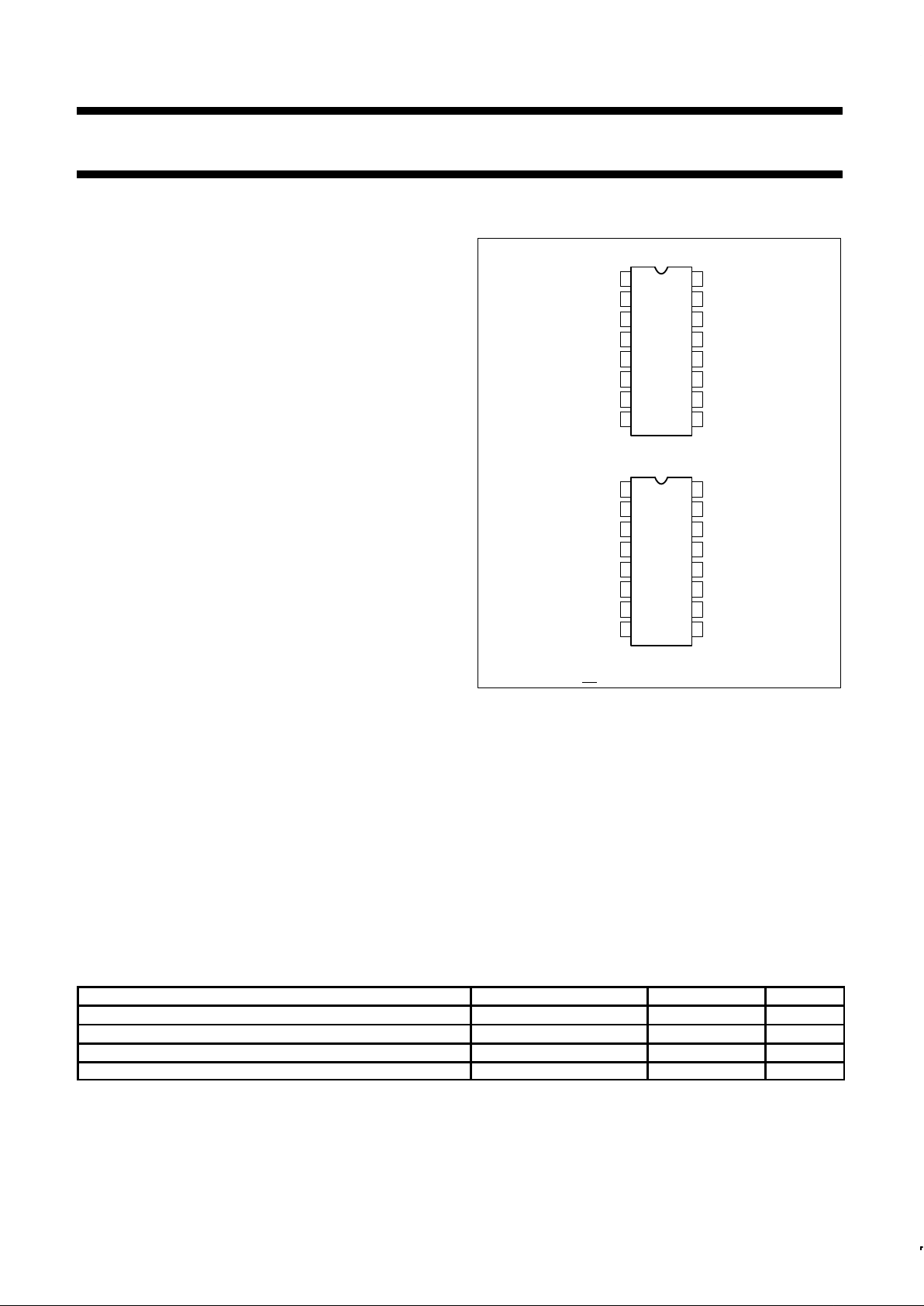
PIN CONFIGURATIONS
F, N Packages
D Package
1
NC
GND
V
EE
COMPEN
TOP VIEW
1
2
3
4
5
6
7
8
9
10
11
12
13
14
16
15
1
2
3
4
5
6
7
8
9
10
11
12
13
14
16
15
V
REF(–)
I
O
MSB A
1
A
2
A
3
A
4
V
REF(+)
V
CC
A8 LSB
A
7
A
6
A
5
A1 MSB
A
2
A
3
A
4
A8 LSB
A
7
A
6
A
5
V
REF(–)
V
REF(+)
COMPEN
NC
GND
V–
I
O
V+
NOTE:
1. SO and
non-standard pinouts.
ORDERING INFORMATION
DESCRIPTION TEMPERATURE RANGE ORDER CODE DWG #
16-Pin Ceramic Dual In-Line Package (CERDIP) -55 to +125°C MC1508-8F 0582B
16-Pin Ceramic Dual In-Line Package (CERDIP) 0 to +70°C MC1408-8F 0582B
16-Pin Plastic Dual In-Line Package (DIP) 0 to +70°C MC1408-8N 0406C
16-Pin Small Outline (SO) Package 0 to +70°C MC1408-8D 0005D
Page 2

Philips Semiconductors Linear Products Product specification
MC1508-8/1408-88-bit multiplying D/A converter
August 31, 1994
738
BLOCK DIAGRAM
CURRENT SWITCHES
5 6 7 8 9 10 11 12
MSB LSB
REFERENCE
CURRENT
AMPLIFIER
14
2
13
16
GND
COMPEN
NPN CURRENT SOURCE PAIR
A
1
A
2
A
3
A
4
A
5
A
6
A
7
A
8
4
BIAS
CURRENT
R-2R LADDER
15
(+)
(–)
V
REF
V
REF
V
CC
3
V
EE
I
O
CIRCUIT DESCRIPTION
The MC1508/MC1408 consists of a reference current amplifier, an
R-2R ladder, and 8 high-speed current switches. For many
applications, only a reference resistor and reference voltage need
be added.
The switches are non-inverting in operation; therefore, a high state
on the input turns on the specified output current component.
The switch uses current steering for high speed, and a termination
amplifier consisting of an active load gain stage with unity gain
feedback. The termination amplifier holds the parasitic capacitance
of the ladder at a constant voltage during switching, and provides a
low impedance termination of equal voltage for all legs of the ladder.
The R-2R ladder divides the reference amplifier current into
binarily-related components, which are fed to the remainder current
which is equal to the least significant bit. This current is shunted to
ground, and the maximum output current is 255/256 of the reference
amplifier current, or 1.992mA for a 2.0mA reference amplifier current
if the NPN current source pair is perfectly matched.
ABSOLUTE MAXIMUM RATINGS
SYMBOL PARAMETER RATING UNIT
V
CC
Positive power supply voltage +5.5 V
V
EE
Negative power supply voltage –16.5 V
V5 – V
12
Digital input voltage 0 to V
CC
V
V
O
Applied output voltage –5.2 to +18 V
I
14
Reference current 5.0 mA
V14, V
15
Reference amplifier inputs VEE to V
CC
P
D
Maximum power dissipation,
T
A
= 25°C (still-air)
1
F package 1190 mW
N package 1450 mW
D package 1080 mW
T
SOLD
Lead soldering temperature (10 sec) 300 °C
T
A
Operating temperature range 300 °C
MC1508 –55 to +125 °C
MC1408 0 to +75 °C
T
STG
Storage temperature range -65 to +150 °C
NOTES:
1. Derate above 25°C, at the following rates: F package at 9.5mW/°C; N package at 11.6mW/°C; D package at 8.6mW/°C
Page 3

Philips Semiconductors Linear Products Product specification
MC1508-8/1408-88-bit multiplying D/A converter
August 31, 1994
739
DC ELECTRICAL CHARACTERISTICS
Pin 3 must be 3V more negative than the potential to which R15 is returned. VCC = +5.0VDC, VEE = –15VDC, V
REF/R14
= 2.0mA unless
otherwise specified. MC1508: T
A
= –55°C to 125°C. MC1408: TA = 0°C to 75°C, unless otherwise noted.
MC1508-8 MC1408-8
SYMBOL
PARAMETER
TEST CONDITIONS
Min Typ Max Min Typ Max
UNIT
E
r
Relative accuracy
Error relative to full-scale
I
O
, Figure 3
±0.19 ±0.19 %
t
S
Settling time
1
To within 1/2 LSB, in-
cludes t
PLH
, TA = +25°C,
Figure 4
70 70 ns
t
PLH
t
PHL
Propagation delay time
Low-to-High
High-to-Low
TA = +25°C, Figure 4 35 100 35 100 ns
TCI
O
Output full-scale current drift –20 –20 ppm/°C
V
IH
V
IL
Digital input logic level (MSB)
High
Low
Figure 5
2.0
0.8
2.0
0.8
V
DC
I
IH
I
IL
Digital input current (MSB)
High
Low
Figure 5
V
IH
= 5.0V
V
IL
= 0.8V
0
–0.4
0.04
–0.8
0
–0.4
0.04
–0.8
mA
I
15
Reference input bias current Pin 15, Figure 5 –1.0 –5.0 –1.0 –5.0 µA
I
OR
Output current range
Figure 5
V
EE
= –5.0V
V
EE
= –7.0V to –15V
0
0
2.0
2.0
2.1
4.2
0
0
2.0
2.0
2.1
4.2
mA
I
O
I
O(min)
Output current
Off-state
Figure 5
V
REF
= 2.000V,
R14 = 1000Ω
All bits low
1.9 1.9902.1
4.0
1.9 1.9902.1
4.0
mA
µA
V
O
Output voltage compliance
Er ≤ 0.19% at
T
A
= +25°C, Figure 5
V
EE
= –5V
V
EE
below –10V
–0.6
+10
–5.5,
+10
–0.55,
+0.5
–5.0,
+0.5
–0.6
+10
–5.5,
+10
–0.55,
+0.5
–5.0,
+0.5
V
DC
SRI
REF
Reference current slew rate Figure 6 8.0 8.0 mA/µs
PSRR(–)
Output current power supply
sensitivity
I
REF
= 1mA 0.5 2.7 0.5 2.7 µA/V
I
CC
I
EE
Power supply current
Positive
Negative
All bits low, Figure 5 +2.5
–6.5
+22
–13
+2.5
–6.5
+22
–13
mA
V
CCR
V
EER
Power supply voltage range
Positive
Negative
TA = +25°C, Figure 5 +4.5
–4.5
+5.0
–15
+5.5
–16.5
+4.5
–4.5
+5.0
–15
+5.5
–16.5
V
DC
P
D
Power dissipation
All bits low, Figure 5
V
EE
= –5.0V
DC
VEE = –15.0V
DC
34
110
170
305
34
110
170
305
mW
NOTES:
1. All bits switched.
Page 4

Philips Semiconductors Linear Products Product specification
MC1508-8/1408-88-bit multiplying D/A converter
August 31, 1994
740
TYPICAL PERFORMANCE CHARACTERISTICS
D-to-A TRANSFER CHARACTERISTICS
I OUTPUT CURRENT (mA)
O
0
1.0
2.0
(00000000) INPUT DIGITAL WORD (11111111)
FUNCTIONAL DESCRIPTION
Reference Amplifier Drive and Compensation
The reference amplifier input current must always flow into Pin 14.
regardless of the setup method or reference supply voltage polarity.
Connections for a positive reference voltage are shown in Figure 1.
The reference voltage source supplies the full reference current.
For bipolar reference signals, as in the multiplying mode, R
15
can be
tied to a negative voltage corresponding to the minimum input level.
R
15
may be eliminated and Pin 15 grounded, with only a small
sacrifice in accuracy and temperature drift.
The compensation capacitor value must be increased with
increasing values of R
14
to maintain proper phase margin. For R
14
values of 1.0, 2.5, and 5.0kΩ, minimum capacitor values are 15, 37,
and 75pF. The capacitor may be tied to either V
EE
or ground, but
using V
EE
increases negative supply rejection. (Fluctuations in the
negative supply have more effect on accuracy than do any changes
in the positive supply.)
A negative reference voltage may be used if R
14
is grounded and
the reference voltage is applied to R
15
, as shown in Figure 2. A
high input impedance is the main advantage of this method. The
negative reference voltage must be at least 3.0V above the V
EE
supply. Bipolar input signals may be handled by connecting R14 to a
positive reference voltage equal to the peak positive input level at
Pin 15.
Capacitive bypass to ground is recommended when a DC reference
voltage is used. The 5.0V logic supply is not recommended as a
reference voltage, but if a well regulated 5.0V supply which drives
logic is to be used as the reference, R
14
should be formed of two
series resistors and the junction of the two resistors bypassed with
0.1µF to ground. For reference voltages greater than 5.0V, a clamp
diode is recommended between Pin 14 and ground.
If Pin 14 is driven by a high impedance such as a transistor current
source, none of the above compensation methods apply and the
amplifier must be heavily compensated, decreasing the overall
bandwidth.
Output Voltage Range
The voltage at Pin 4 must always be at least 4.5V more positive than
the voltage of the negative supply (Pin 3) when the reference current
is 2mA or less, and at least 8V more positive than the negative
supply when the reference current is between 2mA and 4mA. This
is necessary to avoid saturation of the output transistors, which
would cause serious degradation of accuracy.
Philips Semiconductors MC1508/MC1408 does not need a range
control because the design extends the compliance range down to
4.5V (or 8V — see above) above the negative supply voltage
without significant degradation of accuracy. Philips Semiconductors
MC1508/MC1408 can be used in sockets designed for other
manufacturers’ MC1508/MC1408 without circuit modification.
Output Current Range
Any time the full-scale current exceeds 2mA, the negative supply
must be at least 8V more negative than the output voltage. This is
due to the increased internal voltage drops between the negative
supply and the outputs with higher reference currents.
Accuracy
Absolute accuracy is the measure of each output current level with
respect to its intended value, and is dependent upon relative
accuracy, full-scale accuracy and full-scale current drift. Relative
accuracy is the measure of each output current level as a fraction of
the full-scale current after zero-scale current has been nulled out.
The relative accuracy of the MC1508/MC1408 is essentially
constant over the operating temperature range because of the
excellent temperature tracking of the monolithic resistor ladder. The
reference current may drift with temperature, causing a change in
the absolute accuracy of output current; however, the
MC1508/MC1408 has a very low full-scale current drift over the
operating temperature range.
The MC1508/MC1408 series is guaranteed accurate to within
±1/2LSB at +25°C at a full-scale output current of 1.99mA. The
relative accuracy test circuit is shown in Figure 3. The 12-bit
converter is calibrated to a full-scale output current of 1.99219mA;
then the MC1508/MC1408’s full-scale current is trimmed to the
same value with R
14
so that a zero value appears at the error
amplifier output. The counter is activated and the error band may be
displayed on the oscilloscope, detected by comparators, or stored in
a peak detector.
Two 8-bit D-to-A converters may not be used to construct a 16-bit
accurate D-to-A converter. 16-bit accuracy implies a total of ±1/2
part in 65,536, or ±0.00076%, which is much more accurate than the
±0.19% specification of the MC1508/MC1408.
Monotonicity
A monotonic converter is one which always provides an analog
output greater than or equal to the preceding value for a
corresponding increment in the digital input code. The
MC1508/MC1408 is monotonic for all values of reference current
above 0.5mA. The recommended range for operation is a DC
reference current between 0.5mA and 4.0mA.
Settling Time
The worst case switching condition occurs when all bits are
switched on, which corresponds to a low-to-high transition for all
input bits. This time is typically 70ns for settling to within 1/2LSB for
8-bit accuracy. This time applies when R
L
< 500Ω and CO < 25pF.
The slowest single switch is the least significant bit, which typically
turns on and settles in 65ns. In applications where the D-to-A
converter functions in a positive going ramp mode, the worst-case
condition does not occur and settling times less than 70ns may be
realized.
Extra care must be taken in board layout since this usually is the
dominant factor in satisfactory test results when measuring settling
time. Short leads, 100µF supply bypassing for low frequencies,
minimum scope lead length, good ground planes, and avoidance of
ground loops are all mandatory.
Page 5

Philips Semiconductors Linear Products Product specification
MC1508-8/1408-88-bit multiplying D/A converter
August 31, 1994
741
Figure 1. Positive V
REF
A1
A2
A3
A4
A5
A6
A7
A8
5
6
7
8
9
10
11
12
3
MC1508
MC1408
13
14
15
1
2
4
16
SEE TEXT FOR VALUES OF C.
C
R
14
= R
15
(+)V
REF
R
14
R
15
R
L
I
O
V
EE
V
CC
A1
A2
A3
A4
A5
A6
A7
A8
5
6
7
8
9
10
11
12
3
MC1508
MC1408
13
14
15
1
2
4
16
SEE TEXT FOR VALUES OF C.
C
R
14
= R
15
(–)V
REF
R
14
R
15
R
L
I
O
V
EE
V
CC
Figure 2. Negative V
REF
Figure 3. Relative Accuracy
MSB
A1
A2
A3
A4
A5
A6
A7
A8
A9A10 A11 A12
12-BIT
D-TO-A
CONVERTER
ERROR MAX)
0 TO +10V OUTPUT
5k
50k
ERROR (1V = 1%)
NE530
LSB
100
950
5
6
7
8
9
10
11
12
MSB
LSB
MC1508
MC1408
8-BIT
COUNTER
15 16 3 2 1
4
14
13
–
+
1k
C
(±0.02%
V
CC
V
REF
= 2V
V
EE
0.1µF
R
14
Page 6

Philips Semiconductors Linear Products Product specification
MC1508-8/1408-88-bit multiplying D/A converter
August 31, 1994
742
Figure 4. Transient Response and Settling Time
5
6
7
8
9
10
11
12
3
MC1508
MC1408
13
14
15
1
2
4
16
51
C
O
≤ 25pF
R
14
0.1µF
R
L
e
IN
V
EE
V
CC
15pF
0.1µF
1.0k
1.0k
0.1µF
e
O
FOR SETTLING TIME
MEASUREMENT
(ALL BITS
SWITCHED LOW
TO HIGH)
2.4V
0.4V
1.0V
SETTLING TIME
0
0
TRANSIENT
RESPONSE
–100
mV
FOR TURN OFF
MEASUREMENT
USE R
L
to GND
1.4V
R
L
= 50Ω
PIN 4 TO GND
tS = 70ns TYPICAL
TO ±1/2LSB
t
PLH
t
PHL
t
PHL
= t
PLH
= 10ns
RL = 500Ω
e
IN
+2V
DC
Figure 5. Notation Definitions
INPUTS
5
6
7
8
9
10
11
12
3
MC1508
MC1408
13
14
15
1
2
4
16
V
EE
V
CC
THE RESISTOR TIED TO PIN 15 IS TO TEMPERATURE COMPENSATE THE
BIAS CURRENT AND MAY NOT BE NECESSARY FOR ALL APPLICATIONS
V
I
AND II APPLY TO INPUTS A1 THROUGH A
8
IO K
A
1
2
A
2
4
A
3
8
A
4
16
A
5
32
A
6
64
A
7
128
A
8
256
where K
V
REF
R
14
and AN = “1” IF AN IS AT HIGH LEVEL
A
N
= “0” IF AN IS AT LOW LEVEL
DIGITAL
I
EE
I
O
I
15
I
14
R
14
R
15
V
O
OUTPUT
R
L
V
I
I
I
(+)
I
CC
V
REF(+)
(SEE TEXT FOR VALUES OF C.)
TYPICAL VALUES R
14
= R15 = 1k
V
REF
= +2.0V
C = 15pF
A
1
A
2
A
3
A
4
A
5
A
6
A
7
A
8
Figure 6. Reference Current Slew Rate Measurement
2.0mA
5
6
7
8
9
10
11
12
3
13
14
15
1
2
4
16
V
CC
SCOPE
R
L
= 50
V
REF
MC1508
MC1408
V
EE
15pF
1k
1k
SLEWING TIME
10%
90%
0
dI
dt
I
R
L
dV
dt
 Loading...