

Page 1
SEMICONDUCTOR TECHNICAL DATA
Product Preview
Order this document
by MC14LC5447/D
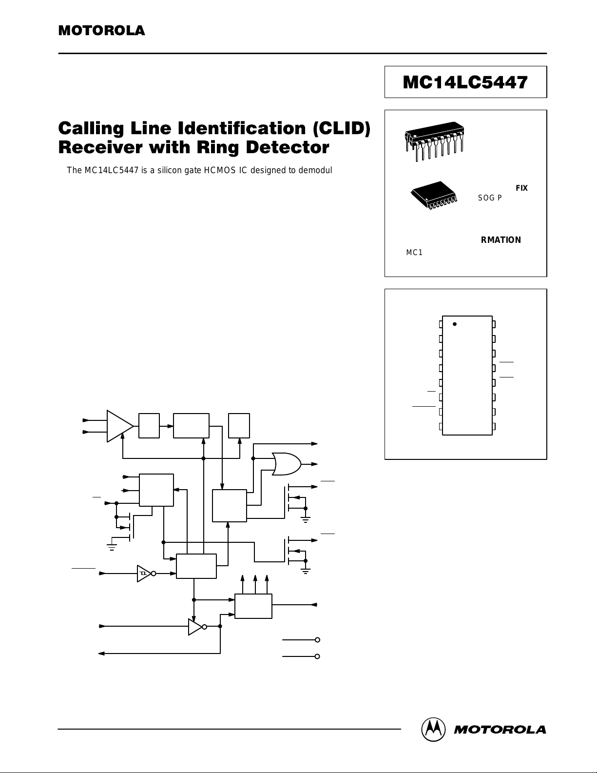
The MC14LC5447 is a silicon gate HCMOS IC designed to demodulate Bell
202 and V.23 1200–baud FSK asynchronous data. The primary application for
this device is in products that will be used to receive and display the calling
number, or message waiting indicator sent to subscribers from participating
central office facilities of the public switched network. The device also contains
a carrier detect circuit and ring detector which may be used to power up the
device.
Applications for this device include adjunct boxes, answering machines,
feature phones, fax machines, and computer interface products.
The MC14LC5447 offers the following performance features.
• Ring Detector On–Chip
• Ring Detect Output for MCU Interrupt
• Power–Down Mode, Less than 1 µA
• Single Supply: + 3.5 to + 6.0 V
• Pin Selectable Clock Frequencies: 3.68 MHz, 3.58 MHz, or 455 kHz
• Two Stage Power–Up for Power Management Control
• Demodulates Bell 202 and V.23
BLOCK DIAGRAM
1
RT
2
–
+
RDI1
RDI2
3
4
6
BPF
RING
DETECT
CIRCUIT
DEMOD
V
AG
VALID
DATA
DETECT
14
15
13
DOR
DOC
CDO
TIP
RING
P SUFFIX
PLASTIC DIP
16
1
16
1
CASE 648
DW SUFFIX
SOG PACKAGE
CASE 751G
ORDERING INFORMATION
MC14LC5447P Plastic DIP
MC14LC5447DW SOG Package
PIN ASSIGNMENT
1
TI
2
RI
3
RDI1
4
RDI2
NC
6
RT
PWRUP
7
8
V
SS
NC = NO CONNECTION
16
15
14
13
125
11
10
9
V
DOC
DOR
CDO
RDO
CLKSIN
OSC
OSC
DD
in
out
12
RDO
INTERNAL
POWER UP
CLOCK
GEN
11
CLKSIN
16
V
DD
8
V
SS
NO CONNECT (5)
MC14LC5447MOTOROLA
in
out
7
10
9
PWRUP
OSC
OSC
This document contains information on a product under development. Motorola reserves the right to change or discontinue this product without notice.
REV 0
7/96
Motorola, Inc. 1996
1
Page 2
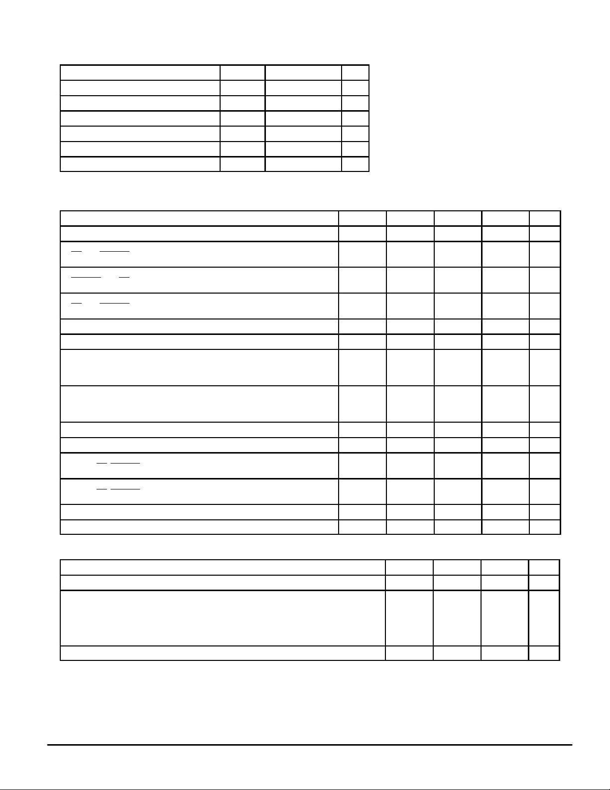
ABSOLUTE MAXIMUM RATINGS
(Voltages referenced to GND, except where noted)
Rating
DC Supply Voltage V
Input Voltage, All Pins V
DC Current Drain Per Pin I ± 10 mA
Power Dissipation P
Operating Temperature Range T
Storage Temperature Range T
Symbol Value Unit
DD
in
D
A
stg
– 0.5 to + 6.0 V
– 0.5 to VDD + 0.5 V
20 mW
0 to + 70 °C
– 40 to + 150 °C
This device contains circuitry to protect the
inputs against damage due to high static voltages or electric fields. However, it is advised that
normal precautions be taken to avoid applications of any voltage higher than maximum rated
voltages to this high impedance circuit. For
proper operation it is recommended that Vin and
V
out
V
out
Reliability of operation is enhanced if unused
inputs are tied to an appropriate logic voltage
level (e.g., either VSS or VDD).
ELECTRICAL CHARACTERISTICS
(All polarities referenced to VSS = 0 V, VDD = + 5 V ± 10%, unless otherwise noted, TA = 0 to + 70°C)
Parameter
DC Supply Voltage V
Supply Current (All Output Pins Unloaded) (See Figure 1)
RT
= 0, PWRUP = 1, XTAL = 3.58 MHz
Supply Current (All Output Pins Unloaded) (See Figure 1)
PWRUP
= 0, RT = Don’t Care, XT AL = 3.58 MHz
Standby Current (All Output Pins Unloaded) (See Figure 1)
RT
= 1, PWRUP = 1
Input Voltage 0 Level (CLKSIN, OSCin) V
Input Voltage 1 Level (CLKSIN, OSCin) V
Output Voltage High: VDD = 5 V (DOR, DOC, OSC
Output Voltage Low: VDD = 5 V (DOR, DOC, OSC
Input Leakage Current (OSCin, CLKSIN, PWRUP, RT, RDI1, and RDI2) I
Output Voltage Low: VDD = 5 V (RDO, RT, CDO) IOL = 2.0 mA V
Input Threshold Voltage Positive Going: VDD = 5 V
(RDI1, RT
Input Threshold Voltage Negative Going: VDD = 5 V
(RDI1, RT
RDI2 Threshold RD2V
TIP/RING Input dc Resistance R
, PWRUP) (See Figure 3)
, PWRUP) (See Figure 3)
out
out
)
IOH = 40 µA
IOH ≤ 1 µA
)
IOL = 1.6 mA
IOL ≤ 1 µA
Symbol Min Typ Max Unit
DD
I
DD
I
DD
I
STBY
IH
V
OH
V
OL
in
OL
V
T+
V
T–
IL
T
in
3.5 5 6 V
— 2.4 3 mA
— 4.0 5.5 mA
— — 1 µA
— — VDD x 0.3 V
VDD x 0.7 — — V
2.4
4.95
— —
— — ±1 µA
— — 0.4 V
2.5 2.75 3.0 V
2.0 2.3 2.6 V
1.0 1.1 1.2 V
— 250 — kΩ
be constrained to the range VSS ≤ (Vin or
) ≤ VDD.
— — V
V
0.4
0.05
ANALOG CHARACTERISTICS (V
Input Sensitivity: TIP and RING (Pins 1 and 2, VDD = + 5 V) – 40 – 45 — dBm
Band–Pass Filter (BPF)
Frequency Response (Relative to 1700 Hz @ 0 dBm) 60 Hz
Carrier Detect Sensitivity — – 48 — dBm
= + 5 V, TA = + 25°C, unless otherwise noted, 0 dBm = 0.7746 Vrms @ 600 Ω)
DD
Characteristic
500 Hz
2700 Hz
≥ 3300 Hz
Min Typ Max Unit
—
—
—
—
– 64
– 4
– 3
– 34
—
dB
—
—
—
MC14LC5447 MOTOROLA
2
Page 3
SWITCHING CHARACTERISTICS (V
Description Symbol Min Typ Max Unit
= + 5 V, CL = 50 pF, TA = + 25°C)
DD
OSC Startup (CLKSIN = 1; 3.579 MHz XTAL) t
Power–Up Low to FSK (Setup Time) t
Carrier Detect Acquisition Time t
End of Data to Carrier Detect High t
TIMING DIAGRAM
0.5
SECOND
RI
RT
RDO
2 SECONDS
THRESHOLD TO KEEP PART ON
t
SUPD
DOSC
SUPD
DAQ
DCH
DATA0101 1
— 2 — ms
15 — — ms
— 14 — ms
8 — — ms
0.5
SECOND
PWRUP
CDO
DOC
DOR
OSC
t
DOSC
t
DAQ
COOKED DATA
RAW DATA
CLOCK 3.58 MHz, 3.6864 MHz, OR 455 kHz
t
DCH
MC14LC5447MOTOROLA
3
Page 4
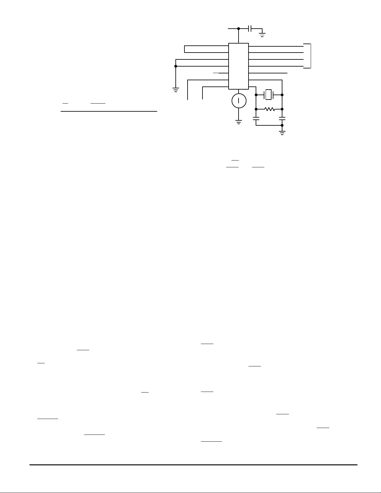
V
TI 1
RI 2
RDI1 3
RDI2 4
NC 5
RT
PWRUP
DD
0.1 µF
15 DOC
16
14 DOR
13 CDO
12 RDO
11 CLKSIN
8
10 OSC
9 OSC
in
out
6
7
V
DD
OPEN
RT
111
0 1 2.4 mA TYP ENABLE
X 0 6.2 mA TYP ENABLE
PWRUP I
µ
A MAX DISABLE
DD
OSC
in
Figure 1. IDD T est Circuit
PIN DESCRIPTIONS
TI
Tip Input (Pin 1)
This input pin is normally connected to the tip side of the
twisted pair. It is internally biased to 1/2 supply voltage when
the device is in the power–up mode. This pin must be dc isolated from the line.
RI
Ring Input (Pin 2)
This input is normally connected to the ring side of the
twisted pair. It is internally biased to 1/2 supply voltage when
the device is in the power–up mode. This pin must be dc isolated from the line.
RDI1
Ring Detect Input 1 (Pin 3)
This input is normally coupled to one of the twisted pair
wires through an attenuating network. It detects energy on
the line and enables the oscillator and precision ring detection circuitry.
RDI2
Ring Detect Input 2 (Pin 4)
This input to the precision ring detection circuit is normally
coupled to one of the twisted pair wires through an attenuating network. A valid ring signal as determined from this
input sends the RDO
RT
Ring Time (Pin 6)
An RC network may be connected to this pin. The RC time
constant is chosen to hold this pin voltage below 2.2 V between the peaks of the ringing signal. RT
power–up control and activates only the circuitry necessary
to determine if the incoming ring is valid.
PWRUP
Power Up (Pin 7)
A logic 0 on the PWRUP
the active mode ready to demodulate incoming data. A
(Pin 12) to a logic 0.
is an internal
input causes the device to be in
3.579 MHz
Ω
10 M
30
pF
30
pF
logic 1 on this pin causes the device to be in the standby
mode, if the RT
trolled by RDO
input pin is at a logic 1. This pin may be con and CDO for auto power–up operation. For
other applications, this pin may be controlled externally .
V
SS
Ground (Pin 8)
Ground return pin is typically connected to the system
ground.
OSC
out
Oscillator Output (Pin 9)
This pin will have either a crystal or a ceramic resonator
tied to it with the other end connected to OSCin.
OSC
in
Oscillator Input (Pin 10)
This pin will have either a crystal or a ceramic resonator
tied to it with the other end connected to OSC
. OSCin may
out
also be driven directly from an appropriate external source.
CLKSIN
Clock Select Input (Pin 11)
A logic 1 on this input configures the device to accept either a 3.579 MHz or 3.6864 MHz crystal. A logic 0 on this pin
configures the part to operate with a 455 kHz resonator.
For crystal and resonator specifications see Table 1.
RDO
Ring Detect Out (Pin 12)
This open–drain output goes low when a valid ringing
signal is detected. RDO
remains low as long as the ringing
signal remains valid. This signal can be used for auto power–
up, when connected to Pin 7.
CDO
Carrier Detect Output (Pin 13)
When low, this open drain output indicates that a valid
carrier is present on the line. CDO
remains low as long as
the carrier remains valid. An 8 ms hysteresis is built in to
allow for a momentary drop out of the carrier. CDO
may be
used in the auto power–up configuration when connected to
PWRUP
.
MC14LC5447 MOTOROLA
4
Page 5

DOR
Data Out Raw (Pin 14)
This pin presents the output of the demodulator whenever
CDO
is low. This data stream includes the alternate 1 and 0
pattern, and the 150 ms of marking, which precedes the
data. At all other times, DOR is held high.
DOC
Data Out Cooked (Pin 15)
This output presents the output of the demodulator when-
ever CDO
is low, and when an internal validation sequence
has been successfully passed. The output does not include
the alternate 1 and 0 pattern. At all other times, DOC is held
high.
V
DD
Positive Power Supply (Pin 16)
The digital supply pin, which is connected to the positive
side of the power supply .
APPLICATIONS INFORMATION
The MC14LC5447 has been designed to be one of the
main functional blocks in products targeted for the CLASS
(Custom Local Area Signaling Service) market. CLASS is a
set of subscriber features now being presented to the consumer by the RBOCs (Regional Bell Operating Companies)
and independent TELCOs. Among CLASS features, such as
distinctive ringing and selective call forwarding, the subscriber will also have available a service known as Calling Number Delivery (CND) and message waiting. With these
services, a subscriber will have the ability to display at a minimum, a message containing the phone number of the calling
party , the date, and the time. A message containing only this
information is known as a single format message, as shown
in Figure 9. An extended message, known as multiple format
message, can contain additional information as shown in
Figure 10.
The interface should be arranged to allow simplex data
transmission from the terminating central office, to the CPE
(Customer Premises Equipment), only when the CPE is in an
on–hook state. The data will be transmitted in the silent period between the first and second power ring after a voice path
has been established.
The data signaling interface should conform to Bell 202,
which is described as follows:
• Analog, phase coherent, frequency shift keying
• Logical 1 (Mark) = 1200 ± 12 Hz
• Logical 0 (Space) = 2200 ± 22 Hz
• Transmission rate = 1200 bps
• Application of data = serial, binary, asynchronous
The transmission level from the terminating C.O. will be
– 13.5 dBm ± 1.0. The expected worst case attenuation
through the loop is expected to be – 20 dB. The receiver
therefore, should have a sensitivity of approximately
– 34.5 dBm to handle the worst case installations.
Additional information on CLASS services can be obtained
from:
BELLCORE CUSTOMER SVS.
1–800–521–2673
201–699–5800 FOREIGN CALLS
201–699–0936 FAX
The document number is: T A–NWT–000030
Title: “Voice Band Data Transmission Interface Generic
Requirements”
Figure 7 is a conceptual design of how the MC14LC5447
can be implemented into a product which will retrieve the incoming message and convert it to EIA–232 levels for transmission to the serial port of a PC. With this message and
appropriate software, the PC can be used to look up the
name and any additional information associated with the caller that had been previously stored.
Figure 8 is a conceptual design of an adjunct unit in parallel with an existing phone. This arrangement gives the subscriber CND service without having to replace existing
equipment.
T able 1. Oscillator Specifications
Clock Select Pin 11 = 1
Crystal Mode Parallel
Frequency 3.579 MHz or 3.6864 MHz
R
f
C1 and C2 30 pF
Source:
Fox Electronics
5570 Enterprise Pkwy.
Ft. Myers, FL 33905
T el. 813–693–0099
Clock Select Pin 11 = 0
Resonator #CSB455J
Frequency 455 kHz ± 0.5%
R
f
C1 and C2 100 pF
Source:
Murata Manufacturing Co. Ltd.
2200 Lake Park Dr.
Smyma, GA 30080
T el. 404–436–1300
NOTE: Motorola cannot recommend one supplier over another
and in no way suggests that this is a complete listing.
10 MΩ
1.0 MΩ
OSC
C1 C2
OSC
in
out
RF
MC14LC5447MOTOROLA
5
Page 6

DESIGN INFORMATION
The circuit in Figure 2 illustrates in greater detail the rela-
tionship between Pins 3, 4, 6, and 7.
The external component values shown in Figure 2 are the
same as those shown in Figures 7 and 8. When VDD is
applied to the circuit in these two figures, the RC network will
charge cap C1 to VDD holding RT
(Pin 7) is also held at VDD, the MC14LC5447 will be in a
power–down mode, and will consume 1 µA of supply current
(max).
The resistor network (R2 – R4) attenuates the incoming
power ring applied to the top of R2. The values given have
been chosen to provide a sufficient voltage at RDI1 (Pin 3) to
turn on the Schmitt–trigger input with approximately a
40 Vrms or greater power ring input from tip and ring. When
VT+ of the Schmitt is exceeded, Q1 will be driven to saturation discharging cap C1 on RT
power–up, with only the portions of the part involved with the
ring signal analysis enabled, including RDI2 (Pin 4). At this
time the MC14LC5447 power consumption is increased to
approximately 2.4 mA (typ).
EXTERNAL
COMPONENTS
PWRUP
RT
RDI1
RDI2
V
DD
TO
BRIDGE
R1
270 k
C1
0.2
470 k
R2
R3
18 k
R4
15 k
Ω
µ
F
Ω
Ω
Ω
Figure 2.
The value of R1 and C1 must be chosen to hold the RT
voltage below the VT+ of the RT
ual cycles of the power ring. The values shown will work for
ring frequencies of 15.3 Hz (min).
With RDI2 now enabled, a portion of the power ring above
1.2 V is fed to the ring analysis circuit. This circuit is a digital
integrator which looks at the duty cycle of the incoming signal. When the input to RDI2 is above 1.2 V, the integrator is
counting up at an 800 Hz rate. When the input to RDI2 falls
below 1.2 V, the integrator counts down at a 400 Hz rate.
(Pin 6) off. If the PWRUP
. This will initialize a partial
INTERNAL
COMPONENTS
7
6
Q1
3
4
V
ref
1.2 V
RING
ANALYSIS
CIRCUIT
Schmitt between the individ-
PWRUP
LOGIC
INTERNAL
POWER–
UP
TO RDO
PIN
pin
3.5
3.25
3.0
2.75
2.5
T
V
2.25
2.0
1.75
1.5
1.25
1.0
2.5 3.0 3.5 4.0 4.5 5.0 5.5 6.0 6.5
V
DD
Figure 3. VDD versus VT+ and V
T–
V
T+
V
T–
A ring is qualified when an internal count of binary 48 is
reached. The ring is disqualified when the count drops to a
binary 32. The number of ring cycles required to qualify the
signal will depend on the amplitude of the voltage presented
to RDI2. The shortest amount of time needed to do the qualification is approximately 60 ms. The shortest amount of time
required for dequalification will be approximately 40 ms.
Once the ring signal is qualified, the RDO
low. This can be fed back to PWRUP
as shown in Figure 7, or
pin will be sent
with a pull–up resistor, can be used as an interrupt to an
MCU as shown in Figure 8. In either case, once the PWRUP
pin is below VT–, the part will be fully powered up, and ready
to receive FSK. During this mode, the device current will increase to approximately 6.2 mA (typ). The state of the RT
pin
is now a “don’t care” as far as the part is concerned. Normally, however, this pin will be allowed to return to VDD.
After the FSK message has been received, the PWRUP
pin can be allowed to return to VDD and the part will return to
the standby mode, consuming less than 1 µA of supply current. The part is now ready to repeat the same sequence for
the next incoming message.
TYPICAL DEMODULATOR PERFORMANCE
The following describes the performance of the
MC14LC5447 demodulator in the presence of noise over a
simulated Bell 3002 telephone loop.
The Bell 3002 loop represents a worst case local telephone loop in North America. The characteristics of this loop,
which affect performance, are high frequency attenuation
and Envelope Delay Distortion (EDD) or group delay .
The minimum receiver sensitivity of the MC14LC5447 under these conditions is typically –
45 dBm.
The MC14LC5447 achieves a Bit Error Rate (BER) of 1 ×
10–5 at a Signal–to–Noise Ratio (SNR) of 15 dB in V.23 operation and at an SNR of 18 dB in Bell 202 operation (see
Figures 4 and 5).
All measurements in dBm are referenced to 600 Ω: 0 dBm
= 0.7746 Vrms.
All measurements were taken using the MC145460EVK
evaluation board.
MC14LC5447 MOTOROLA
6
Page 7

Electronic file not available for
this figure. To view the complete
document, order it from the
Literature Center.
Electronic file not available for
this figure. To view the complete
document, order it from the
Literature Center.
Figure 4. MC14LC5447 V.23 Operation
(Typical BER vs SNR)
500 pF
TIP
10 k
10 k
Ω
Ω
V
DD
500 pF
RING
TI
RI
RDI1
RDI2
N/C
RT
Figure 5. MC14LC5447 Bell 202 Operation
(Typical BER vs SNR)
V
DD
1
2
3
4
5
6
7PWRUP
16
8
0.1
µ
f
DOC
15
DOR
14
CDO
13
RDO
12
CLKSIN
11
10
9
OSC
in
OSC
out
3.579 MHz
10 M
Ω
V
DD
30 pF30 pF
Figure 6. Full–Time Power without Ring Detect
MC14LC5447MOTOROLA
7
Page 8

APPLICATION CIRCUIT
TIP
C1
PROTECTION
NETWORK
RING
C2
NOTE: C1 and C2 ≥ 0.2 µF required for line
isolation. C1 through C4 are 250 V min,
non–polarized.
Figure 7. Partial Implementation of PC Interface to Tip and Ring
500 pF
C3
1N4004x4
500 pF
C4
470 k
15 k
10 k
10 k
Ω
MC14LC5447
V
Ω
Ω
18 k
Ω
Ω
270 k
0.2
+5 V
Ω
µ
F
DD
TI 1
RI 2
RDI1 3
RDI2 4
NC 5
RT 6
PWRUP
7
+5 V
16
8
30 pF
4.7 M
0.33 µF
µ
F
0.1
15 DOC
14 DOR
13 CDO
12 RDO
11 CLKSIN
10 OSC
9 OSC
3.579 MHz
Ω
in
out
10 M
TO PC
TO PC
V
DD
MC145407
Ω
30 pF
RI
RT
RDO
PWRUP
CDO
DOR
DOC
OSC
FIRST RING
2 SECONDS
NOTE 1
0.5
SEC
0101 1
NOTE 1
NOTE 2
DATA
3.58 MHz, 3.6864, OR 455 kHz
DATA
DATA
0.5
SEC
SECOND RING
2 SECONDS
NOTE 3
NOTES:
1. Wired ‘OR’ RDO
2. Overlap of RDO edge with CDO edge to ensure part stays in PWRUP determined by RC time constant on RDO, PWRUP ,
and CDO
3. Part reverts to PWR ON
with CDO.
pin.
, on rising edge of RDO since there is no CDO.
Timing Diagram for Figure 7
MC14LC5447 MOTOROLA
8
Page 9

500 pF
C3
APPLICATION CIRCUIT
10 k
Ω
0.1
2 k
2 k
Ω
Ω
V
DD
µ
F
TIP
RING
0.2
0.2
TO PHONE
FIRST RING
2 SECONDS
C1
C2
500 pF
µ
F
µ
F
470 k
18 k
15 k
C4
7
MCU
DISPLAY
16
15 DOC
14 DOR
13 CDO
12 RDO
11 CLKSIN
MC14LC5447
10 OSC
9 OSC
8
INTERRUPT
3.68 MHz
in
out
V
DD
10 k
Ω
Ω
Ω
Ω
270 k
0.2 µF
V
DD
Ω
TI 1
RI 2
RDI1 3
RDI2 4
NC 5
RT 6
PWRUP
Figure 8. Adjunct Box Concept for Calling Number Display
0.5
SEC
0.5
SEC
SECOND RING
2 SECONDS
RI
RT
RDO
PWRUP
CDO
DOC
DOR
OSC
NOTES:
1. MCU must assert PWRUP
2. No data detected, MCU powers down the MC14LC5447.
INTERRUPT
FOR MCU
NOTE 1
3.58 MHz, 3.6864 MHz, OR 455 kHz
to MC14LC5447.
0101 1
Timing Diagram for Figure 8
DATA
NOTE 1
NOTE 2
DATA
DATA
MC14LC5447MOTOROLA
9
Page 10

2 s
0.5s495
ms
4 s 2 s
0.5
s
STD RING/20 Hz
STD RING/20 Hz
2 s
DATA WORD
MESSAGE
TYPE WORD
30 BYTES/600 Hz
01010101
250 ms
BITS8BITS
MO – DAY – HOUR – MINUTE – NUMBER
04 – 15 – 16 – 21 – 512 555 1212
MARKS
70
ms
8
COUNT
DATA
175 ms
144 BITS MAX
Figure 9. Single Message Format
0.5
s
VARIABLE
4 s
CHECK
SUM
8
BITS
2 s
0.5
s
MESSAGE
TYPE WORD
MESSAGE
LENGTH WORD
30 BYTES/600 Hz
8
BITS8BITS8BITS8BITS
PARAMETER
TYPE WORD
PARAMETER
LENGTH WORD
DATA
70
ms
8
BITS8BITS
PARAMETER
TYPE WORD
DATAMARKS
LENGTH WORD
DATA
PARAMETER
250 ms VARIABLE
01010101
CALLING NAME
Figure 10. Multiple Message Format
CHECK
SUM
144 DATA BITS
MO – DAY – HOUR – MINUTE – NUMBER
04 – 15 – 16 – 21 – 512 555 1212
8
BITS
MC14LC5447 MOTOROLA
10
Page 11

P ACKAGE DIMENSIONS
P SUFFIX
PLASTIC DIP
CASE 648–08
–A–
916
B
18
F
H
G
D
16 PL
0.25 (0.010) T
C
S
SEATING
–T–
PLANE
K
M
A
J
M
DW SUFFIX
SOG PACKAGE
CASE 751G–02
NOTES:
1. DIMENSIONING AND TOLERANCING PER ANSI
Y14.5M, 1982.
2. CONTROLLING DIMENSION: INCH.
3. DIMENSION L TO CENTER OF LEADS WHEN
FORMED PARALLEL.
4. DIMENSION B DOES NOT INCLUDE MOLD FLASH.
5. ROUNDED CORNERS OPTIONAL.
DIM MIN MAX MIN MAX
L
M
A 0.740 0.770 18.80 19.55
B 0.250 0.270 6.35 6.85
C 0.145 0.175 3.69 4.44
D 0.015 0.021 0.39 0.53
F 0.040 0.70 1.02 1.77
G 0.100 BSC 2.54 BSC
H 0.050 BSC 1.27 BSC
J 0.008 0.015 0.21 0.38
K 0.110 0.130 2.80 3.30
L 0.295 0.305 7.50 7.74
M 0 10 0 10
S 0.020 0.040 0.51 1.01
MILLIMETERSINCHES
____
–A–
16 9
D16X
M
0.010 (0.25) B
A
T
G14X
–B– P8X
81
S
S
C
K
0.010 (0.25)
–T–
SEATING
PLANE
NOTES:
1. DIMENSIONING AND TOLERANCING PER ANSI
Y14.5M, 1982.
2. CONTROLLING DIMENSION: MILLIMETER.
M
M
B
J
F
R
X 45
_
M
3. DIMENSIONS A AND B DO NOT INCLUDE MOLD
PROTRUSION.
4. MAXIMUM MOLD PROTRUSION 0.15 (0.006) PER
SIDE.
5. DIMENSION D DOES NOT INCLUDE DAMBAR
PROTRUSION. ALLOWABLE DAMBAR
PROTRUSION SHALL BE 0.13 (0.005) TOTAL IN
EXCESS OF D DIMENSION AT MAXIMUM
MATERIAL CONDITION.
DIM MIN MAX MIN MAX
A 10.15 10.45 0.400 0.411
B 7.40 7.60 0.292 0.299
C 2.35 2.65 0.093 0.104
D 0.35 0.49 0.014 0.019
F 0.50 0.90 0.020 0.035
G 1.27 BSC 0.050 BSC
J 0.25 0.32 0.010 0.012
K 0.10 0.25 0.004 0.009
M 0 7 0 7
____
P 10.05 10.55 0.395 0.415
R 0.25 0.75 0.010 0.029
INCHESMILLIMETERS
MC14LC5447MOTOROLA
11
Page 12

Motorola reserves the right to make changes without further notice to any products herein. Motorola makes no warranty , representation or guarantee regarding
the suitability of its products for any particular purpose, nor does Motorola assume any liability arising out of the application or use of any product or circuit, and
specifically disclaims any and all liability, including without limitation consequential or incidental damages. “T ypical” parameters which may be provided in Motorola
data sheets and/or specifications can and do vary in different applications and actual performance may vary over time. All operating parameters, including “Typicals”
must be validated for each customer application by customer’s technical experts. Motorola does not convey any license under its patent rights nor the rights of
others. Motorola products are not designed, intended, or authorized for use as components in systems intended for surgical implant into the body, or other
applications intended to support or sustain life, or for any other application in which the failure of the Motorola product could create a situation where personal injury
or death may occur. Should Buyer purchase or use Motorola products for any such unintended or unauthorized application, Buyer shall indemnify and hold Motorola
and its officers, employees, subsidiaries, affiliates, and distributors harmless against all claims, costs, damages, and expenses, and reasonable attorney fees
arising out of, directly or indirectly, any claim of personal injury or death associated with such unintended or unauthorized use, even if such claim alleges that
Motorola was negligent regarding the design or manufacture of the part. Motorola and are registered trademarks of Motorola, Inc. Motorola, Inc. is an Equal
Opportunity/Affirmative Action Employer.
How to reach us:
USA/EUROPE/Locations Not Listed: Motorola Literature Distribution; JAPAN: Nippon Motorola Ltd.; Tatsumi–SPD–JLDC, 6F Seibu–Butsuryu–Center,
P.O. Box 20912; Phoenix, Arizona 85036. 1–800–441–2447 or 602–303–5454 3–14–2 Tatsumi Koto–Ku, Tokyo 135, Japan. 03–81–3521–8315
MFAX: RMF AX0@email.sps.mot.com – TOUCHT ONE 602–244–6609 ASIA/PACIFIC: Motorola Semiconductors H.K. Ltd.; 8B Tai Ping Industrial Park,
INTERNET: http://Design–NET.com 51 Ting Kok Road, Tai Po, N.T., Hong Kong. 852–26629298
MC14LC5447 MOTOROLA
12
◊
*MC14LC5447/D*
MC14LC5447/D
 Loading...