

Page 1
MOTOROLA
SEMICONDUCTOR TECHNICAL DATA
MC14LC5003
128 Segment LCD Drivers
CMOS
The MC14LC5003/5004 are 128-segment, multiplexed-by-four LCD Drivers. The two devices are functionally the same except for their data input
protocols. The MC14LC5003 uses a serial interface data input protocol. The
device may be interf aced to the MC68HCXX product families using a minimal
amount of software (see example). The MC14LC5004 has a IIC interface and
has essentially the same protocol, except that the device sends an ac knowledge bit back to the transmitter after each eight-bit byte is received.
MC14LC5004 also has a “read mode”, whereby data sent to the device ma y
be retrieved via the IIC bus.
The MC14LC5003/MC14LC5004 drives the liquid-crystal displays in a multiplexed-b y-four configuration. The device accepts data from a microprocessor or other serial data source to drive one segment per bit. The chip does
not have a decoder , allo wing f or the fle xibility of f ormatting the segment data
externally .
Devices are independently addressable via a two-wire (or three-wire) communication link which can be common with other peripheral devices.
The MC14LC5003/MC14LC5004 are low cost version of MC145003 and
MC145004 without cascading function.
• Drives 128 Segments Per Package
• May Be Used with the Following LCDs: Segmented Alphanumeric,
Bar Graph, Dot Matrix, Custom
• Quiescent Supply Current: 30 A @ 2.7 V V
• Operating Voltage Range: 2.7 to 5.5 V
• Operating Temperature Range: -40 to 85C
• Separate Access to LCD Drive Section’s Supply Voltage to Allow f or Tem-
perature Compensation
• See Application Notes AN1066 and AN442
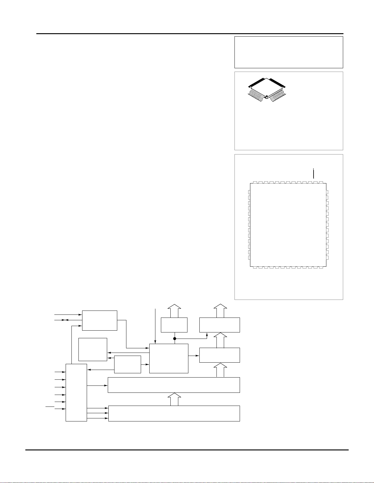
BLOCK DIAGRAM
OSC1
OSC2
OSCILLATOR
DD
BP1-BP4 FP1-FP32
V
LCD
DRIVERS
DRIVERS
MC14LC5004
1
52
ORDERING INFORMATION
MC14LC5003FU QFP
MC14LC5004FU QFP
MCC14LC5003 BARE DIE
MCC14LC5004 BARE DIE
PIN ASSIGNMENT
DD
OSC2
V
FP18
FP17
BP2
BP1
FP16
FP15
NC
OSC1
52 51 50 49 48 47 46 45 44 43 42 41 40
FP32
1
FP31
2
FP30
3
FP29
4
FP28
5
FP27
6
FP26
7
FP25
8
FP24
9
FP23
10
FP22
11
FP21
12
FP20
13
14 15 16 17 18 19 20 21 22 23 24 25 26
NC
FP19
NC=NO CONNECTION
BP3
LCD
V
BP4A0A1
SS
V
FP14
QFP
FU SUFFIX
CASE 848B
ENB
NC
A2
39
38
37
36
35
34
33
32
31
30
29
28
27
NC
FP11
FP13
FP12
Din
DCLK
NC
FP1
FP2
FP3
FP4
FP5
FP6
FP7
FP8
FP9
FP10
REV 2
10/96
DCLK
D
A0
A1
A2
ENB
FRAME
SYNC
GENERATOR
POR
in
DATA AND ADDRESS
CONTROL AND TIMING
LCD VOLTAGE
WAVEFORM
AND TIMING
GENERATOR
128-BIT LATCH
128-BIT SHIFT REGISTER
128 - 32
MULTIPLEX
MC14LC5003 • MC14LC5004MOTOROLA
3–3
Page 2
ABSOLUTE MAXIMUM RATINGS (Voltages Referenced to VSS)
Symbol Parameter Value Unit
V
V
V
in osc
T
DC Supply Voltage - 0.5 to + 6.5 V
DD
Input Voltage, Din, and Data Clock - 0.5 to 15 V
in
Input Voltage, OSCin of Master - 0.5 to VDD+ 0.5 V
I
DC Input Current, per Pin ± 10 mA
in
T
Operating Temperature Range - 40 to + 85 °C
A
Storage Temperature Range - 65 to + 150 °C
stg
* Maximum Ratings are those values beyond which damage to the device may occur. Func-
tional operation should be restricted to the limits in the Electrical Characteristics tables or
Pin Descriptions section.
This device contains protection circuitry
to guard against damage due to high static
voltages or electric fields. Howev er , precautions must be taken to avoid applications of
any voltage higher than maximum rated voltages to this high-impedance circuit. This
device may be light sensitive. Caution
should be taken to avoid exposure of this
device to any light source during normal operation. This device is not radiation protected.
ELECTRICAL CHARACTERISTICS (Voltages Referenced to V
Characteristic
Symbol
Output Drive Current — Frontplanes
VO = 0.15 V I
VO = 2.65 V I
VO = 1.72 V I
VO = 1.08 V I
VO = 0.15 V I
VO = 5.35 V I
VO = 3.52 V I
VO = 1.98 V I
FH
I
FL
FH
I
FL
FH
I
FL
FH
I
FL
FH
I
FL
FH
I
FL
FH
I
FL
FH
I
FL
Supply Standby Currents (No Clock)
IDD = Standby @ I
= Standby @ I
I
LCD
= Standby @ I
I
DD
= Standby @ I
I
LCD
out
out
out
out
= 0 µA
= 0 µA
= 0 µA
= 0 µA
I
DDS
I
LCDS
I
DDS
I
LCDS
, TA= 25C)
SS
V
DD
V
5
5
5
5
5
5
5
5
5
5
5
5
5
5
5
5
2.7
—
5.5
—
V
LCD
V Min Typical Max
2.7
2.7
2.7
2.7
2.7
2.7
2.7
2.7
5.5
5.5
5.5
5.5
5.5
5.5
5.5
5.5
—
2.7
—
5.5
260
260
-240
-240
-40
—
40
—
600
600
-520
-520
-35
—
55
—
—
—
—
—
—
—
—
—
—
—
—
—
—
—
—
—
—
—
—
—
—
—
—
—
Unit
µA
—
—
—
—
—
-1.5
—
2
—
—
—
—
—
-1.5
—
1
µA
30
800
50
1500
Supply Currents (f
= Quiescent @ I
I
DD
I
= Quiescent @ loading = 270pF
DD
= Quiescent @ I
I
DD
= Quiescent @ loading = 270pF
I
DD
= Quiescent @ I
I
LCD
= Quiescent @ I
I
LCD
) = 110 kHz
OSC
= 0 µA, no loading
out
= 0 µA, no loading
out
= 0 µA, no loading
out
= 0 µA, no loading
out
I
I
I
I
I
LCDQ
I
LCDQ
Input Current I
Input Capacitance C
MC14LC5003 • MC14LC5004
3–4
DDQ
DDQ
DDQ
DDQ
in
µA
2.7
2.7
5.5
5.5
—
—
—
—
—
—
2.7
5.5
—
—
—
—
—
—
30
—
170
—
—
—
—
70
—
400
40
70
— — -0.1 — 0.1 µA
in
— — — — 7.5 pF
(continued)
MOTOROLA
Page 3

ELECTRICAL CHARACTERISTICS (Continued)
V
V
DD
Characteristic
Symbol
Frequencies
OSC2 Frequency @ R1; R1 = 200 kΩ
BP Frequency @ R1
OSC2 Frequency @ R2; R2 = 996 kΩ
Average DC Offset Voltage (BP Relative to FP) V
Input Voltage “0” Level V
“1” Level V
f
OSC2
f
BP
f
OSC2
V
V
OO
2.8
IL
5.5
IL
2.8
IH
5.5
IH
Output Drive Current — Backplanes VO = 2.65 V IBH*
I
BL
VO = 0.15 V I
VO = 1.08V I
VO = 1.72 V I
VO = 5.35 V I
VO = 0.15 V I
VO = 1.98 V I
VO = 3.52 V I
Pulse Width, Data Clock (Figure 1) t
DCLK Rise/Fall Time (Figure 1) tr, t
Setup Time, Din to DCLK (Figure 2) t
Hold Time, Din to DCLK (Figure 2) t
DCLK Low to ENB High (Figure 3) t
ENB High to DCLK High (Figure 3) t
ENB High Pulse Width (Figure 3) t
ENB Low to DCLK High (Figure 3) t
BH
I
BL
BH
I
BL
BH
I
BL
BH
I
BL
BH
I
BL
BH
I
BL
BH
I
BL
w
f
su
h
h
rec
w
su
NOTE: Timing for Figures 1, 2, and 3 are design estimates only.
* For a time (t = 4/OSC FREQ.) after the backplane waveform changes to a new voltage level, the circuit is maintained in the high-current state to
allow the load capacitances to charge quickly. The circuit is then returned to the low-current state until the next voltage change.
LCD
V
5
5
5
V Min Typical Max
5
5
5
100
100
23
—
—
—
150
150
33
Unit
kHz
Hz
kHz
5 2.8 -50 — +50 mV
5
5
5
5
5
2.8
5
2.8
5
2.8
5
2.8
5
2.8
5
2.8
5
2.8
5
2.8
5
5.5
5
5.5
5
5.5
5
5.5
5
5.5
5
5.5
5
5.5
5
5.5
5
3
5
3
5
3
5
3
5
3
5
3
5
3
5
3
—
—
2
3.85
-240
-240
260
260
40
—
-40
—
-520
-520
600
600
55
—
-35
—
50
100
—
—
0
0
30
60
10
20
10
20
50
100
10
20
—
—
—
—
—
—
—
—
—
—
—
—
—
—
—
—
—
—
—
—
—
—
—
—
—
—
—
—
—
—
—
—
—
—
—
—
0.85
1.65
—
—
—
—
—
—
—
2
—
-1
—
—
—
—
—
1
—
-1
—
—
20
120
—
—
—
—
—
—
—
—
—
—
—
—
V
µA
ns
µs
ns
ns
ns
ns
ns
ns
MC14LC5003 • MC14LC5004MOTOROLA
3–5
Page 4

SWITCHING WAVEFORMS
CLK
90%
50%
10%
t
f
t
r
V
DD
D
in
50%
GND
t
w
t
w
CLK
Figure 1. Figure 2.
ENB
CLK
50%
50%
FIRST
CLK
t
w
t
su
LAST
CLK
t
w
t
h
t
rec
V
DD
GND
V
DD
GND
Figure 3.
VALID
V
DD
GND
t
su
50%
t
h
V
DD
GND
MC14LC5003 • MC14LC5004
3–6
MOTOROLA
Page 5
FUNCTIONAL DESCRIPTION
The MC14LC5003/MC14LC5004 has essentially two sections which operate asynchronously from each other; the data
input and storage section and the LCD drive section. The LCD
drive and timing is derived from the oscillator, while the data
input and storage is controlled by the Data In (D
(DCLK), Address (A0, A1, A2), and Enable (
), Data Clock
in
ENB) pins.
Data is shifted serially into the 128-bit shift register and arranged into four consecutive b locks of 32 parallel data bits. A
time-multiplex of the four backplane drivers is made (each
backplane driver becoming active then inactive one after another) and, at the start of each backplane active period, the
corresponding block of 32 bits is made available at the frontplane drivers. A high input to a plane driver turns the driver
on, and a low input turns the driver off.
Figure 4 shows the sequence of backplanes. Figure 5 shows
the possible configurations of the frontplanes relative to the
backplanes. When a backplane driver is on, its output s witches
from V
to 2/3 V
output switches from 0 V to V
from 2/3 V
to 0 V, and when it is off, it switches from 1/3 V
LCD
. When a frontplane driver is on, its
LCD
, and when it is off, it switches
LCD
LCD
to 1/3 V
LCD
.
LCD
The LCD drive and timing section provides the multiplex signals and backplane driver input signals and formats the frontplane and backplane waveforms.
The address pins are used to uniquely distinguish LCD driver
from any other chips on the same bus and to define LCD driver
as the “master” in the system. There must be one master in any
system.
The enable pin may be used as a third control line in the
communication bus. It may be used to define the moment
when the data is latched. If not used, then the data is latched
after 128 bits of data have been received.
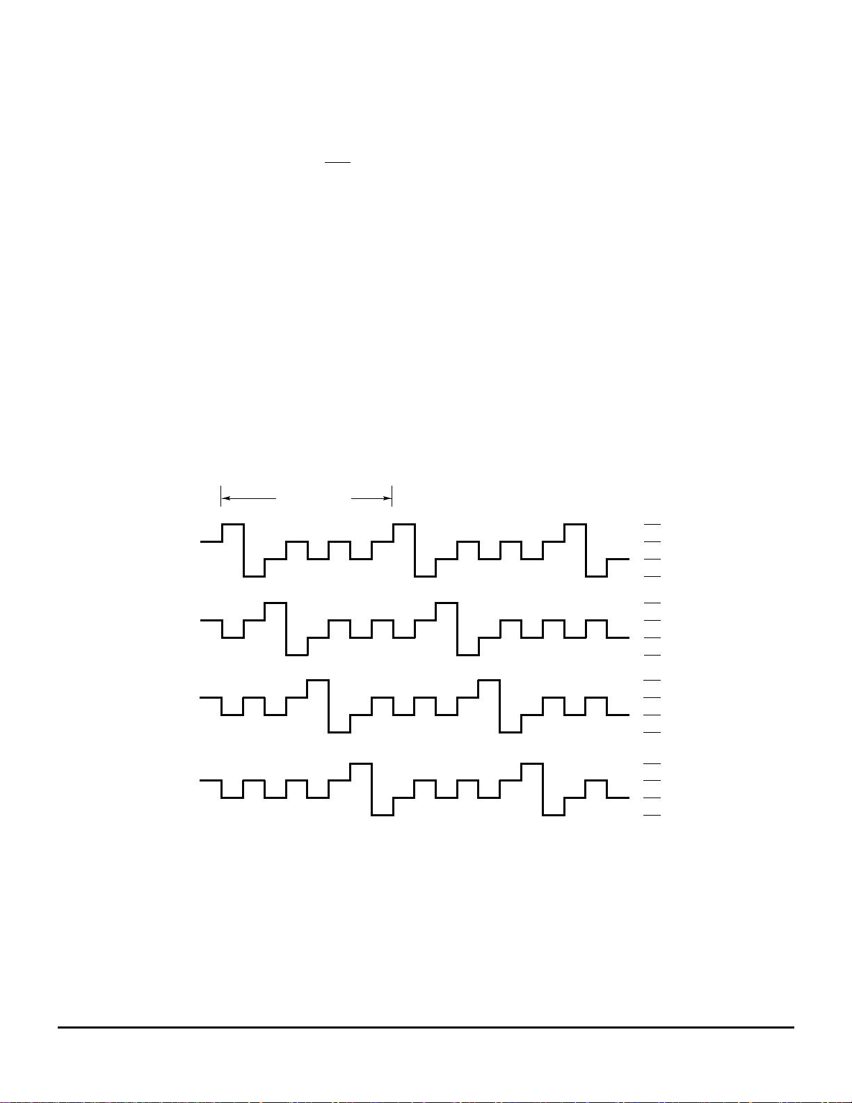
BP1
BP2
BP3
BP4
TIME FRAME
Figure 4. Backplane Sequence
V
LCD
2/3 (V
1/3 (V
0 V
V
LCD
2/3 (V
1/3 (V
0 V
V
LCD
2/3 (V
1/3 (V
0 V
V
LCD
2/3 (V
1/3 (V
0 V
LCD
LCD
LCD
LCD
LCD
LCD
LCD
LCD
)
)
)
)
)
)
)
)
MC14LC5003 • MC14LC5004MOTOROLA
3–7
Page 6

BP1
TIME FRAME
V
LCD
BP1
TIME FRAME
V
LCD
FP DATA
BITS
4321
0000
1000
0100
1100
0010
1010
0110
1110
0 V
V
LCD
2/3 (V
1/3 (V
0 V
V
LCD
2/3 (V
1/3 (V
0 V
V
LCD
2/3 (V
1/3 (V
0 V
V
LCD
2/3 (V
1/3 (V
0 V
V
LCD
2/3 (V
1/3 (V
0 V
V
LCD
2/3 (V
1/3 (V
0 V
V
LCD
2/3 (V
1/3 (V
0 V
V
LCD
2/3 (V
1/3 (V
0 V
LCD
LCD
LCD
LCD
LCD
LCD
LCD
LCD
LCD
LCD
LCD
LCD
LCD
LCD
LCD
LCD
0 V
V
FP DATA
)
)
)
)
BITS
4321
0001
1001
LCD
2/3 (V
1/3 (V
0 V
V
LCD
2/3 (V
1/3 (V
LCD
LCD
LCD
LCD
)
)
)
)
0 V
V
LCD
)
)
0101
2/3 (V
1/3 (V
LCD
LCD
)
)
0 V
V
LCD
)
)
1101
2/3 (V
1/3 (V
LCD
LCD
)
)
0 V
V
LCD
)
)
0011
2/3 (V
1/3 (V
LCD
LCD
)
)
0 V
V
LCD
)
)
1011
2/3 (V
1/3 (V
LCD
LCD
)
)
0 V
V
LCD
)
)
0111
2/3 (V
1/3 (V
LCD
LCD
)
)
0 V
V
LCD
)
)
1111
2/3 (V
1/3 (V
LCD
LCD
)
)
0 V
MC14LC5003 • MC14LC5004
3–8
Figure 5. Frontplane Combinations
MOTOROLA
Page 7

PIN DESCRIPTIONS
A0-A2
Address Inputs (Pins 42-44)
The devices hav e to receive a correct address before they
will accept data. Three address pins (A2, A1, A0) are used to
define the states of the three programmable bits of
MC14LC5003/MC14LC5004’s 8-bit address.
The address is 0111vwxy where v, w, x represent A2, A1,
and A0 respectively. Where v, w, x= 0, then A2, A1, and A0
should be tied to 0 V. Where v, w, x= 1, then A2, A1, and A0
should be tied to V
The address pins must be tied to V
device as a master.
Note: In applications where the circuit will be isolated from
external manual interference the system designer may take
advantage of the self-programming feature. Upon power-on,
address pins which are left open-circuit will be charged to VDD.
However, care must be taken not to inadvertently discharge
the pins after power-on since the address may then be lost. A
similar feature is also available on the
The configuration A0, A1, A2 = 000 should not be used. This
does not give a valid address and is reserved for Motorola’s
use only. All three address pins should never be tied to 0 V
simultaneously.
ENB
Enable Input (Pin 41)
If the
ENB pin is tied to VDD, the MC14LC5003/
MC14LC5004 will always latch the data after 128 bits have
been received. The latched data is multiplex ed and f ed to the
frontplane drivers for display. If external control of this latching
function is required, then the
followed by one high pulse on
quired. (This may be useful in a system where one MC145003/
MC145004 is permanently addressed and only the last 128
bits of data sent are required to be latched for display). The
pulse on the
DCLK, D
ENB pin must occur while DCLK is high.
in
Data Clock and Data Input (Pins 38, 39)
Address input and data input controls. SeeData Input Protocol sections for relevant option.
OSC1, OSC2
Oscillator Pins (Pins 51, 50)
To use the on-board oscillator, an external resistor should
be connected between OSC1 and OSC2. Optionally, the
OSC1 pin may be driven by an externally generated clock
signal.
A resistor of 680 k connected between OSC1 and OSC2
pins gives an oscillator frequency of about 30 kHz, giving
approximately 30 Hz as seen at the LCD driver outputs. A
resistor of 200 k gives about 100 kHz, which results in 100Hz
at the driver outputs. LCD manufacturers recommend an LCD
drive frequency of between 30 Hz and 100 Hz. See Figure 6.
DD
.
CAUTION
. This defines the
DD
NOTE
ENB pin.
ENB pin should be held low,
ENB when data display is re-
10 M
1 M
100 k
10 k
1 k 10 k 100 k 1 M
EXTERNAL RESISTOR VALUE
OSCILLATOR FREQUENCY
10 M
Figure 6. Oscillator Frequency vs. Load Resistance
(Approximate)
FP1-FP32
Frontplane Drivers (Pins 36-27, 25-22, 19-15, 13-1)
Frontplane driver outputs.
BP1-BP4
Backplane Drivers (Pins 48-45)
Backplane driver outputs.
V
LCD
LCD Driver Supply (Pin 20)
Power supply input for LCD drive outputs. May be used to
supply a temperature-compensated voltage to the LCD drive
section, which can be separate from the logic voltage supply,
V
.
DD
V
DD
Positive Power Supply (Pin 49)
This pin supplies power to the main processor interface and
logic portions of the device. The voltage range is 2.7 to 5.5 V
with respect to the V
For optimum performance, V
using a low inductance capacitor mounted very closely
V
SS
SS
pin.
should be bypassed to
DD
to these pins. Lead length on this capacitor should be minimized.
V
SS
Ground (Pin 21)
Common ground.
DATA INPUT PROTOCOL
Two-wire communication bus DCLK, Din; three-wire communication bus DCLK, D
MC14LC5003 — SERIAL INTERFACE DEVICE (FIGURE 7)
Before communication with an MC14LC5003 can begin, a
start condition must be set up on the bus by the transmitter.
To establish a start condition, the transmitter must pull the
data line low while the clock line is high. The “idle” state for
the clock line and data line is the high state.
After the start condition has been established, an eight-bit
address should be sent by the transmitter . If the address sent
corresponds to the address of the MC14LC5003 then on each
, ENB.
in
MC14LC5003 • MC14LC5004MOTOROLA
3–9
Page 8

successive clock pulse, the addressed device will accept a
data bit.
ENB pin is permanently high, then the addressed
If the
MC14LC5003’s internal counter latches the data to be displayed after 128 data bits hav e been received. Otherwise, the
control of this latch function may be overridden b y holding the
ENB line low until the new data is required to be displayed,
then a high pulse should be sent on the
pulse must be sent during DCLK high (clock idle).
To end communication with an MC14LC5003, a stop condition should be set up on the bus (or another start condition
may be set up if another communication is desired). Note that
the communication channel to an addressed device may be
left open after the 128 data bits have been sent by not setting
up a stop or a start condition. In such a case, the 129th rising
DCLK edge, which normally would be used to set up the stop
or start condition, is ignored by the MC14LC5003 and data
continues to be received on the 130th rising DCLK. The latch
function continues to work as normal (i.e., data is be latched
either after each block of 128 data bits has been received or
under external control as required).
At any time during data transmission, the transfer may be
interrupted with a stop condition. Data transmission may be
resumed with a start condition and resending the address.
MC14LC5004 — IIC DEVICE (FIGURE 8)
Before communication with an MC14LC5004 can begin, a
start condition must be set up on the bus by the controller. To
establish a start condition, the controller must pull the data
line low while the clock line is high.
After the start condition has been established, an eight-bit
address should be sent by the controller followed b y an e xtra
clock pulse while the data line is left high. In this option, only
the seven most significant bits of the address are used to
uniquely define devices on the bus, the least significant bit is
used as a read/write control: if the least significant bit is 0,
then the controller writes to the LCD driver; if it is 1, then the
ENB line. The high
controller reads from the LCD driver’s 128-bit shift register on
a first-in first-out basis. If the seven most significant address
bits sent correspond to the address of the LCD driver then the
addressed LCD driver responds by sending an “acknowledge”
bit back to the controller (i.e., the LCD driver pulls the data line
low during the extra clock pulse supplied by the controller). If
the least significant address bit was 0, then the controller
should continue to send data to the LCD driver in blocks of
eight bits followed by an extra ninth clock pulse to allow the
LCD driver to pull the data line D
If the least significant address bit was 1, then the LCD driver
sends data back to the controller (the clock is supplied by the
controller). After each successive group of eight bits sent, the
LCD driver leaves the data line high for one pulse.
ENB pin is permanently high, then the addressed
If the
MC14LC5004’s internal counter latches the data to be displayed after 128 data bits have been received. Otherwise the
control of this latch function may be overridden b y holding the
ENB line low until the new data is required to be displayed,
then a high pulse should be sent on the
pulse must be sent during DCLK high (clock idle).
T o end comm unication with an MC14LC5004, a stop condition should be set up on the bus (or another start condition
may be set up if another communication is desired). Note that
the communication channel to an addressed device may be
left open after the 128 data bits have been sent by not setting
up a stop or a start condition. In such a case the rising DCLK
edge which comes after all 128 data bits have been sent and
after the last acknowledge-related clock pulse has been made
is ignored; data continues to be received on the following
DCLK high. The latch function continues to work as normal
(i.e., data is latched either after each block of 128 data bits
has been received or under external control as required).
At any time during data transmission, the transfer may be
interrupted with a stop condition. Data transmission may be
resumed with a start condition and resending the address.
low as an acknowledgment.
in
ENB line. The high
MC14LC5003 • MC14LC5004
3–10
MOTOROLA
Page 9

129TH DCLK HIGH:
(DOES NOT SHIFT DATA)
START
BUT MUST BE DURING DCLK HIGH.
ENABLE PULSE MAY OCCUR AS REQUIRED
A2 A1 A0 BP4 BP3 BP2 BP1 BP4 BP3 BP2 BP1
FP1 FP2
Figure 7a. Data Input—MC14LC5003
BP
4321
432143214321432143214321
x
D
FP32
Figure 7b. Serial 128 Bits Data
FP1 FP2 FP3 FP4 FP5 FP6
(BPi, FPj) ON
(BPi, FPj) OFF
→
→
0
in
x: 1
START 8-BITS ADDRESS 128-BITS DATA
in
D
DCLK
ENB
(IF USED)
Figure 7. MC14LC5003(SERIAL INTERFACE DEVICE)
MC14LC5003 • MC14LC5004MOTOROLA
3–11
Page 10

LAST DCLK PULSE
(DOES NOT SHIFT DATA)
BUT MUST BE DURING DCLK HIGH.
ENABLE PULSE MAY OCCUR AS REQUIRED;
LAST DCLK PULSE
(DOES NOT SHIFT DATA)
ACKNOWLEDGE
ENTIRE CLK FOR
STOP
LEFT HIGH BY DRIVER
LEFT HIGH
BY CONTROLLER
FP1 FP2
LEFT HIGH
BY CONTROLLER
(LOW-ORDER BIT 02=0)
A2 A1 A0 BP4 BP3 BP2 BP1 BP4 BP3 BP2 BP1
ACKNOWLEDGE
ENTIRE CLK FOR
ACKNOWLEDGE
ENTIRE CLK FOR
CONTINUES TO CLOCK DATA AND ACKNOWLEDGE
PULLED LOW BY DRIVER STOP
PULLED LOW BY DRIVER
CONTINUES TO CLOCK DATA AND ACKNOWLEDGE
ACKNOWLEDGE
ENTIRE CLK FOR
ACKNOWLEDGE
ENTIRE CLK FOR
ADDRESS ACKNOWLEDGED BY DRIVER LEFT HIGH BY DRIVER
(LOW-ORDER BIT=1)
in
D
WRITE TO LCD DRIVER
(FROM
CONTROLLER)
DCLK
MC14LC5003 • MC14LC5004
3–12
START 8-BITS ADDRESS 8-BITS DATA
in
D
DRIVER)
(FROM LCD
ENB
(IF USED)
READ FROM LCD DRIVER
in
D
(FROM
Figure 8 . Data Input MC14LC5004 (IIC Device)
CONTROLLER)
DCLK
START 8-BITS ADDRESS 8-BITS DATA
in
D
DRIVER)
(FROM LCD
MOTOROLA
Page 11

BP1-BP4
680 k
ON BUS
FP1-FP32 BP1-BP4
LIQUID CRYSTAL DISPLAY
FP32
FP31
FP1-FP32
FP30
FP29
FP28
FP27
FP26
FP25
FP24
FP23
FP22
FP21
FP20
OSC1
FP19
OSC2
FP18
DD
V
FP17
BP1
FP16
BP2
FP15VV
A0A1A2
BP3
BP4
LCD DRIVER
LCD
SS
FP14
FP13
FP12
ENB
DCLK
FP10
FP11
D
FP1
FP2
FP3
FP4
FP5
FP6
FP7
FP8
FP9
in
CONTROLLER
Figure 9. Application Example
SS
DD
V
V
LCD
V
DATA
CLOCK
STROBE
MC14LC5003 • MC14LC5004MOTOROLA
3–13
Page 12

APPLICATION INFORMATION
Figure 10 shows an interface example.
Example shows a semi-automatic SPI Mode (only start and stop conditions are done in non-SPI Mode). It contains the software
to use HC11 with MC14LC5003 in manual SPI Mode.
V
DD
OSC1
OSC2
FP1-FP32
R = 470 k
MC68HC11
V
DD
MOSI
1 k
SCK
SS
BP1-BP4
1/4 MUX DISPLAY
D
in
DCLK
ENB
A0
A1 A2
MC14LC5003
Figure 10. Interface Example Between MC68HC11 and MC14LC5003
1
2 ;=======CONSTANTS=================================================
3 0000 T extram equ $A000 ;$A000 for 8K RAM
4 0000 T stack equ $00FF ;last RAM byte
5 0000 T intofs equ $1000 ;Internal Registers
6 0000 T data equ $08
7 0000 T clock equ $10
8 0000 T enable equ $20
9 0000 T portd equ 8
10
11
12 ;=======PROGRAM BEGIN=============================================
13 A000 T org extram ;Program into RAM
14 A000 N 8E00FF cold lds #stack ;set stack pointer
15 A003 M 8638 ldaa #$38 ;set of MOSI,SS,SCK
16 A005 T B71009 staa $1009 ;DDRD
17 A008 M C611 ldab #17
18 A00A N CEA05E ldx #send
19 A00D T BDA010 jsr spi
20 A010 T end cold
21
22 A010 U 18CE1000 spi ldy #intofs
23 A014 J 181D0820 bclr portd,y #enable ;EN = 0
24 A018 T BDA031 jsr start ;start condition
25 A01B X A600 again ldaa 0 , x ;SPI Mode Use
26 A01D T B7102A staa $102A ;SPDR
27 A020 L 181F2980FB brclr $29,y,#$80,*
28 A025 H 08 inx ;next DATA
29 A026 H 5A decb
30 A027 R 26F2 bne again
31 A029 J 181C0820 bset portd,y #enable
32 A02D T BDA04C jsr stop ;stop condition
33 A030 H 39 rts
34
35 A031 M 8633 start ldaa #$33 ;Normal Mode
36 A033 T B71028 staa $1028 ;SPCR
MC14LC5003 • MC14LC5004
3–14
MOTOROLA
Page 13

37 A036 J 181C0808 bset portd,y #data ;DATA = 1
38 A03A J 181C0810 bset portd,y #clock ;CLK = 1
39 A03E J 181D0808 bclr portd,y #data ;DATA = 0
40 A042 J 181D0810 bclr portd,y #clock ;CLK = 0
41 A046 M 8673 ldaa #$73 ;SPI Mode
42 A048 T B71028 staa $1028 ;SPCR
43 A04B H 39 rts
44 A04C M 8633 stop ldaa #$33 ;Normal Mode
45 A04E T B71028 staa $1028 ;SPCR
46 A051 J 181D0808 bclr portd,y #data ;DATA = 0
47 A055 J 181C0810 bset portd,y #clock ;CLK = 1
48 A059 J 181C0808 bset portd,y #data ;DATA = 0
49 A05D H 39 rts
50
51 A05E T 7E send fcb $007E ;LCD Driver Address
52 A05F T F0 fcb $00f0 ;Data to sent
53 A060 T F0 fcb $00f0
54 A061 T F0 fcb $00f0
55 A062 T F0 fcb $00f0
56 A063 T F0 fcb $00f0
57 A064 T F0 fcb $00f0
58 A065 T F0 fcb $00f0
59 A066 T F0 fcb $00f0
60 A067 T F0 fcb $00f0
61 A068 T F0 fcb $00f0
62 A069 T F0 fcb $00f0
63 A06A T F0 fcb $00f0
64 A06B T F0 fcb $00f0
65 A06C T F0 fcb $00f0
66 A06D T F0 fcb $00f0
67 A06E T F0 fcb $00f0
68 A06F H 39 rts
69
70 ;=======PROGRAM END===============================================
Example 1. Semi-Automatic SPI Method
Figure 11 shows another interface example.
Example 2 contains the software to use HC05 with MC14LC5003 in serial data interface.
V
DD
OSC1
OSC2
FP1-FP32
MC68HC05
V
DD
DOUT
SCK
STROBE
1 k
BP1-BP4
1/4 MUX DISPLAY
D
in
DCLK
ENB
A0
A1 A2
MC14LC5003
R = 470 k
Figure 11. Interface Example Between MC68HC05 and MC14LC5003
MC14LC5003 • MC14LC5004MOTOROLA
3–15
Page 14

PORTC EQU $02 PORTC
DDRC EQU $06 PORTDC
SEN EQU $07 ENABLE PIN, PC7
SCL EQU $06 CLOCK PIN, PC6
SDA EQU $05 DATA PIN, PC5
DOUT EQU $FF OUTPUT DATA
ORG $0050
W1 RMB 1
COUNT RMB 1
ORG $1FFE ADDRESS OF RESET VECTOR OF MC68HC805C4
FCB #$01 RESET VECTOR
FCB #$00
*** Main Program start at 0100 ***
ORG $0100
START LDA #DOUT SET DATA LINE OUTPUT
STA DDRC
AGAIN
LDX #$00
BSET SDA,PORTC IDLE STATE
BSET SCL,PORTC CLOCK AND DATA ARE HIGH
READY BSET SEN,PORTC EN=1
LDA #$11 SET ADDRESS AND 8 CHARACTERS
STA W1
BCLR SDA,PORTC START CONDITION, DATA LOW WHILE CLOCK HIGH
LBYTE CLC
LDA #$08
STA COUNT 8 BITS TO SHIFT
LDA SEND,X GET A BYTE
INCX
LBIT BCLR SCL,PORTC CLOCK LOW
ROLA
BCC DZERO DATA BIT=0 ?
BSET SDA,PORTC NO, BIT=1 AND DATA HIGH
JMP CLKHI
DZERO BCLR SDA,PORTC DATA LOW
CLKHI BSET SCL,PORTC CLOCK HIGH
DEC COUNT
BNE LBIT
DEC W1
BNE LBYTE LAST BYTE ?
STOP BCLR SCL,PORTC
BCLR SDA,PORTC STOP CONDITION
BSET SCL,PORTC DATA GOES HIGH WHILE CLOCK HIGH
BSET SDA,PORTC
BCLR SEN,PORTC EN=0
RTS
*** End of Program ***
*** LCD Address and Data ***
SEND
FCB $7E LCD DRIVER ADDRESS
FCB $FF, $FF, $FF, $FF, $FF, $FF, $FF, $FF DATA TO SENT
FCB $FF, $FF, $FF, $FF, $FF, $FF, $FF, $FF
RTS
MC14LC5003 • MC14LC5004
3–16
Example 2. Serial Data Interface Method
MOTOROLA
Page 15

PACKAGE DIMENSIONS
QFP
FU SUFFIX
CASE 848B-02
L
39
40
-A-
L
DETAIL A
52
27
26
0.05 (0.002) A-B
V
D
S S
A-B
C
M
0.20 (0.008)
D
S S
-D-
14
B
A-B
H
M
0.20 (0.008)
B
1
-D-
13
B
B
0.20 (0.008) A-B D
0.05 (0.002)
M
A-B
V
0.20 (0.008)
M
H
C
A-B D
S
S
-A,B,D-
DETAIL A
S
S
F
C
M
E
DETAIL C
J
N
-C-
SEATING
PLANE
DATUM
PLANE
-H-
H
DETAIL C
DATUM
-H-
PLANE
D
S
BASE METAL
0.10 (0.004)
G
M
0.02 (0.008) A-B
D
C
M
S
SECTION B-B
U
T
R
K
W
X
NOTES:
1.DIMENSIONING AND TOLERANCING PER ANSI
Y14.5M, 1982.
2.CONTROLLING DIMENSION: MILLIMETER.
3.DATUM PLANE -H- IS LOCATED A T BO TTOM OF
LEAD AND IS COINCIDENT WITH THE LEAD
WHERE THE LEAD EXITS THE PLASTIC BODY
AT THE BOTTOM OF THE PARTING LINE.
4.DATUMS -A-, -B- AND -D- TO BE DETERMINED
AT DATUM PLANE -H-.
Q
5.DIMENSIONS S AND V TO BE DETERMINED AT
SEATING PLANE -C-.
6.DIMENSIONS A AND B DO NOT INCLUDE MOLD
PROTRUSION. ALLOWABLE PROTRUSION IS
0.25 (0.010) PER SIDE. DIMENSIONS A AND B
DO INCLUDE MOLD MISMATCH AND ARE
DETERMINED AT DATUM PLANE -H-.
7.DIMENSION D DOES NOT INCLUDE DAMBAR
PROTRUSION. ALLOWABLE DAMBAR
PROTRUSION SHALL BE 0.08 (0.003) TOTAL IN
EXCESS OF THE D DIMENSION AT MAXIMUM
MATERIAL CONDITION. DAMBAR CANNOT BE
LOCATED ON THE LOWER RADIUS OR THE
FOOT.
MILLIMETERS INCHES
DIM MIN MAX MIN MX
A 9.90 10.10 0.390 0.398
B 9.90 10.10 0.390 0.398
C 2.10 2.45 0.083 0.096
D 0.22 0.38 0.009 0.015
E 2.00 2.10 0.079 0.083
F 0.22 0.33 0.009 0.013
G 0.65 BSC 0.026 BSC
H -- 0.25 -- 0.010
J 0.13 0.23 0.005 0.009
K 0.65 0.95 0.026 0.037
L 7.80 REF 0.307 REF
M 5˚ 10˚ 5˚ 10˚
N 0.13 0.17 0.005 0.007
Q0˚ 7˚ 0˚ 7˚
R 0.13 0.30 0.005 0.012
S 12.95 13.45 0.510 0.530
T 0.13 -- 0.005 -U0˚ -- 0˚ --
V 12.95 13.45 0.510 0.530
W 0.35 0.45 0.014 0.018
X 1.6 REF 0.063 REF
MC14LC5003 • MC14LC5004MOTOROLA
3–17
Page 16

PIN 1
+Y
-Y
BOND PAD LAYOUT
+X-X
HONG KONG I.C.
DESIGN CENTER
©
PIN NO. PIN NAME
1 FP32 -736.002 929.199
2 FP31 -736.002 781.999
3 FP30 -736.002 634.799
4 FP29 -736.002 487.599
5 FP28 -736.002 340.399
6 FP27 -736.002 193.199
7 FP26 -736.002 45.999
8 FP25 -736.002 -101.201
9 FP24 -736.002 -248.401
10 FP23 -736.002 -395.601
11 FP22 -736.002 -542.801
12 FP21 -736.002 -690.001
13 FP20 -736.002 -837.201
14 NC N/A N/A
15 FP19 -736.002 -1205.601
16 FP18 -588.802 -1205.601
17 FP17 -441.602 -1205.601
18 FP16 -294.402 -1205.601
19 FP15 -147.202 -1205.601
20 V
21 V
22 FP14 294.398 -1205.601
23 FP13 441.598 -1205.601
24 FP12 588.798 -1205.601
25 FP11 735.998 -1205.601
26 NC N/A N/A
LCD
SS
COORDINATES
XY
0.000 -1205.600
147.200 -1205.600
BOND PAD COORDINATES
PIN NO. PIN NAME
27 FP10 735.998 -837.201
28 FP9 735.998 -690.001
29 FP8 735.998 -542.801
30 FP7 735.998 -395.601
31 FP6 735.998 -248.401
32 FP5 735.998 -101.201
33 FP4 735.998 45.999
34 FP3 735.998 193.199
35 FP2 735.998 340.399
36 FP1 735.998 487.599
37 NC 736.000 634.800
38 DCLK 736.000 782.000
39 D
40 NC N/A N/A
41
42 A2 588.800 1205.600
43 A1 441.600 1205.600
44 A0 294.400 1205.600
45 BP4 147.198 1205.599
46 BP3 -0.002 1205.599
47 BP2 -147.202 1205.599
48 BP1 -294.402 1205.599
49 V
50 OSC2 -588.800 1205.600
51 OSC1 -736.000 1205.600
52 NC N/A N/A
IN
ENB 736.000 1205.600
DD
Die size : 78 x 119 mil
(1 mil ~ 25.4m)
COORDINATES
XY
736.000 929.200
-441.600 1205.600
2
MC14LC5003 • MC14LC5004
3–18
Dimemsions in m
MOTOROLA
 Loading...