

Page 1
Device
Operating
Temperature Range
Package
SEMICONDUCTOR
TECHNICAL DATA
QUAD LOW POWER
LINE DRIVER
ORDERING INFORMATION
MC14C88BP
MC14C88BD
TA = – 40° to +85°C
Plastic DIP
SO–14
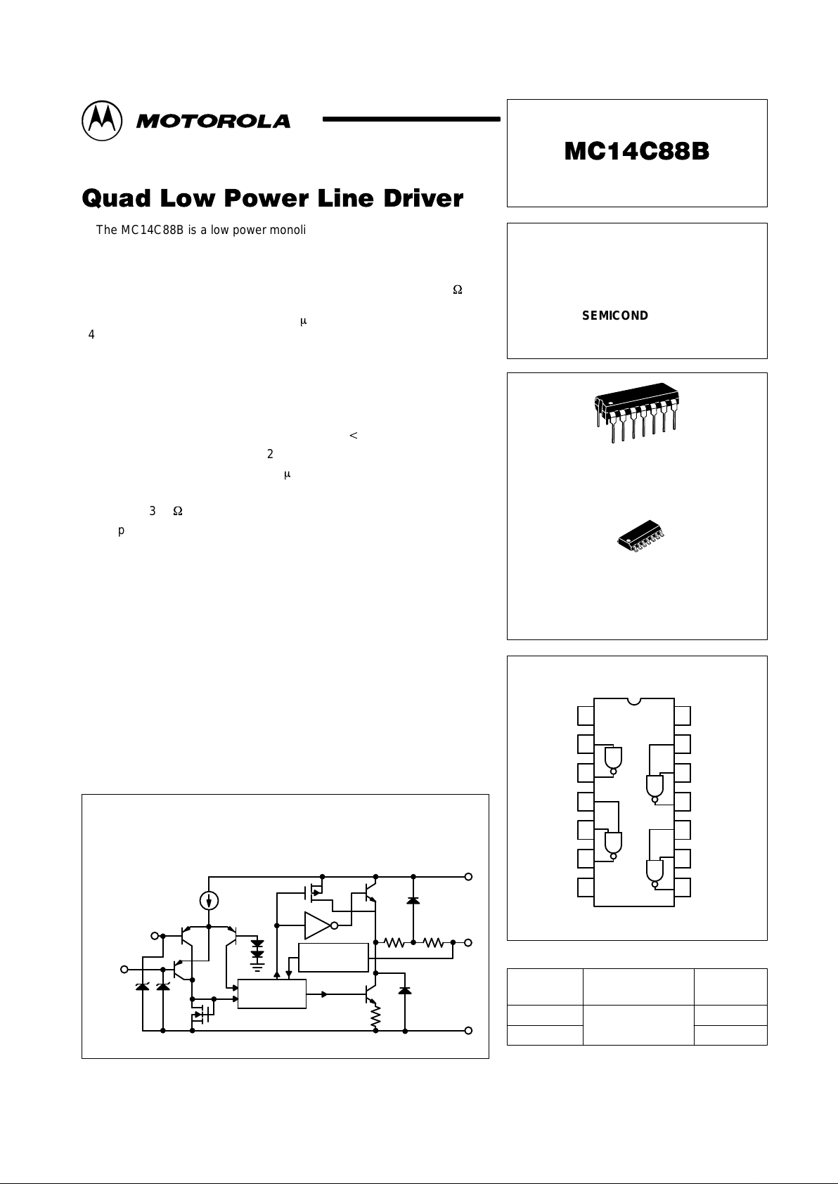
PIN CONNECTIONS
Order this document by MC14C88B/D
P SUFFIX
PLASTIC PACKAGE
CASE 646
D SUFFIX
PLASTIC PACKAGE
CASE 751A
(SO–14)
(Top View)
Output A
Input A
1
V
EE
2
3
Input B1
Input B2
Output B
Gnd
4
5
6
7
14
Input D1
Input D2
12
13
V
CC
Input C1
Output D
Input C2
Output C
8
9
11
10
1
MOTOROLA ANALOG IC DEVICE DATA
The MC14C88B is a low power monolithic quad line driver, using BiMOS
technology, which conforms to EIA–232–D, EIA–562, and CCITT V.28. The
inputs feature TTL and CMOS compatibility with minimal loading. The
outputs feature internally controlled slew rate limiting, eliminating the need
for external capacitors. Power off output impedance exceeds 300 W, and
current limiting protects the outputs in the event of short circuits.
Power supply current is less than 160 mA over the supply voltage range of
±4.5 to ±15 V. EIA–232–D performance is guaranteed with a minimum
supply voltage of ±6.5 V.
The MC14C88B is pin compatible with the MC1488, SN75188,
SN75C188, DS1488, and DS14C88. This device is available in 14 pin plastic
DIP, and surface mount packaging.
Features:
• BiMOS Technology for Low Power Operation (
t
5.0 mW)
• Meets Requirements of EIA–232–D, EIA–562, and CCITT V.28
• Quiescent Current Less Than 160
m
A
• TTL/CMOS Compatible Inputs
• Minimum 300
W
Output Impedance when Powered Off
• Supply Voltage Range: ±4.5 to ±15 V
• Pin Equivalent to MC1488
• Current Limited Output: 10 mA Minimum
• Operating Ambient Temperature: –40° to 85°C
Representative Block Diagram
(Each Driver)
V
EE
39 39
Switching
Control
Output250
V
CC
Slew Rate
Control
45
Input 2
Input 1
Motorola, Inc. 1996 Rev 0
Page 2
MC14C88B
2
MOTOROLA ANALOG IC DEVICE DATA
MAXIMUM RATINGS (T
A
= +25°C, unless otherwise noted.)
Rating Symbol Value Unit
Power Supply Voltage
V
CC(max)
V
EE(min)
(VCC – VEE)
max
V
CC
V
EE
VCC – V
EE
+17
–17
34
Vdc
Input Voltage (All Inputs) V
in
VEE–0.3, VEE+39 Vdc
Applied Output Voltage, when VCC=VEE0
0 V
Applied Output Voltage, when VCC=VEE=0 V
V
X
VEE–6.0 V , VCC+6.0 V
±15
Vdc
Output Current I
O
Self Limiting mA
Operating Junction Temperature T
J
– 65, + 150 °C
Devices should not be operated at these limits. The “Recommended Operating Conditions” table provides
for actual device operation.
RECOMMENDED OPERATING CONDITIONS
Characteristic Symbol Min Typ Max Unit
Power Supply Voltage V
CC
V
EE
+4.5
–15
–
–
+15
–4.5
Vdc
Input Voltage (All Inputs) V
in
0 – V
CC
Vdc
Applied Output Voltage (VCC=VEE=0 V) V
O
–2.0 0 +2.0 Vdc
Output DC Load R
L
3.0 – 7.0 kΩ
Operating Ambient Temperature Range T
A
–40 – +85 °C
All limits are not necessarily functional concurrently.
ELECTRICAL CHARACTERISTICS (–40°C
p
TA p+85°C, unless otherwise noted.)*
Characteristic Symbol Min Typ Max Unit
Supply Current (I
out
= 0, see Figure 2)
ICC @ 4.75 V p VCC, –VEE p 15 V
Outputs High
Outputs Low
I
EE
Outputs High
Outputs Low
ICC
(OH)
ICC
(OL)
IEE
(OH)
IEE
(OL)
–
–
–160
–160
–
–
–
–
160
160
–
–
µA
Output Voltage – High, Vin p0.8 V (RL = 3.0 kΩ , see Fi gure 3)
VCC = +4.75 V , VEE = –4.75 V
VCC = +5.0 V , VEE = –5.0 V
VCC = +6.5 V , VEE = –6.5 V
VCC = +12 V , VEE = –12 V
VCC = +13.2 V , VEE = –13.2 V (RL = ∞)
Output Voltage – Low, Vin q2.0 V
VCC = +4.75 V , VEE = –4.75 V
VCC = +5.0 V , VEE = –5.0 V
VCC = +6.5 V , VEE = –6.5 V
VCC = +12 V , VEE = –12 V
VCC = +13.2 V , VEE = –13.2 V (RL = ∞)
V
OH
V
OL
3.7
4.0
5.0
10
–
–
–
–
–
–13.2
3.8
4.3
6.1
10.5
13.2
–3.8
–4.2
–6.0
–10.5
–13.2
–
–
–
–
13.2
–3.7
–4.0
–5.0
–10
–
Vdc
Output Short Circuit Current** (see Figure 4) (VCC =VEE = 15 V )
Normally High Output, shorted to ground
Normally Low Output, shorted to ground
I
OS
–35
+10
–
–
–10
+35
mA
Output Source Resistance
(VCC = VEE = 0 V, –2.0 V p V
out
p+2.0 V)
R
O
300 – – Ω
Input Voltage
Low Level
High Level
V
IL
V
IH
0
2.0
–
–
0.8
V
CC
Vdc
* Typicals reflect performance @ TA = 25°C
** Only one output shorted at a time, for not more than 1 second.
Page 3
MC14C88B
3
MOTOROLA ANALOG IC DEVICE DATA
ELECTRICAL CHARACTERISTICS (continued) (–40°C
p
TA p +85°C, unless otherwise noted.)*
Characteristic Symbol Min Typ Max Unit
Input Current
Vin = 0 V, VCC = VEE = 4.75 V
Vin = 0 V, VCC = VEE = 15 V
Vin = 4.5 V , VCC = VEE = 4.75 V
Vin = 4.5 V , VCC = VEE = 15 V
I
in
–10
–10
0
0
–0.1
–0.1
+0.1
+0.1
0
0
+10
+10
µA
TIMING CHARACTERISTICS (–40°C
p
TA p +85°C, unless otherwise noted.)*
Characteristic
Symbol Min Typ Max Unit
Output Rise Time
VCC = 4.75 V , VEE = –4.75 V
–3.3 V pVO p 3.3 V
CL = 15 pF
CL = 1000 pF
–3.0 V pVO p 3.0 V
CL = 15 pF
CL = 1000 pF
VCC = 12.0 V , VEE = –12.0 V
–3.0 V pVO p 3.0 V
CL = 15 pF
CL = 2500 pF
10% pVO p 90%
CL = 15 pF
t
R1
t
R2
t
R3
0.22
0.22
0.20
0.20
0.20
0.20
0.53
0.66
1.52
0.51
1.16
0.62
0.82
1.41
2.1
2.1
1.5
1.5
1.5
1.5
3.2
µs
Output Fall Time
VCC = 4.75 V , VEE = –4.75 V
3.3 V pVO p –3.3 V
CL = 15 pF
CL = 1000 pF
3.0 V pVO p –3.0 V
CL = 15 pF
CL = 1000 pF
VCC = 12.0 V , VEE = –12.0 V
3.0 V pVO p –3.0 V
CL = 15 pF
CL = 2500 pF
90% pVO p 10%
CL = 15 pF
t
F1
t
F2
t
F3
0.22
0.22
0.20
0.20
0.20
0.20
0.53
0.93
1.28
0.72
1.01
0.70
0.94
1.71
2.1
2.1
1.5
1.5
1.5
1.5
3.2
µs
Output Slew Rate, 3.0 kΩ t RL t 7.0 kΩ , 15 pF t CL t 2500 pF S
R
4.0 – 30 V/µs
Propagation Delay A (CL = 15 pF, see Figure 1)
VCC = 12.0 V , VEE = –12.0 V
Input to Output – Low to High
Input to Output – High to Low
Propagation Delay B (CL = 15 pF, see Figure 1)
VCC = 4.75 V , VEE = –4.75 V
Input to Output – Low to High
Input to Output – High to Low
t
PLH
t
PHL
t
PLH
t
PHL
–
–
–
–
0.9
2.3
0.4
1.5
3.0
3.5
2.0
2.5
µs
* Typicals reflect performance @ TA = 25°C
Page 4

MC14C88B
4
MOTOROLA ANALOG IC DEVICE DATA
Figure 1. Timing Diagram
t
R3
V
OH
t
F3
t
F1
t
F2
t
PHL
1.5 V
0 V
S.G.
3.0 V
V
OUT
C
L
3.0 k
V
CC
V
EE
S.G.
–3.3 V
t
PLH
90%
3.3 V
3.0 V
–3.0 V
10%
t
R2
t
R1
0 V
V
OL
NOTES: S.G. set to: f = 20 kHz for Propogation Delay A
and f = 64 kHz for Propagation Delay B; Duty
Cycle = 50%; tR, tFp
5.0 ns
V
out
STANDARDS COMPLIANCE
The MC14C88 is designed to comply with EIA–232–D
(formerly RS–232), the newer EIA–562 (which is a higher
speed version of the EIA–232), and CCITT’s V.28. EIA–562
was written around modern integrated circuit technology,
whereas EIA–232 retains many of the specs written around
the electro–mechanical circuitry in use at the time of its
creation. Yet the user will find enough similarities to allow a
certain amount of compatibility among equipment built to the
two standards. Following is a summary of the key
specifications relating to the systems and the drivers.
Parameter EIA–232–D EIA–562
Maximum Data Rate 20 kbaud 38.4 kbaud Asynchronous
64 kbaud Synchronous
Maximum Cable Length 50 feet Based on cable capacitance/data rate
Maximum Slew Rate
p
30 V/µs anywhere on the waveform
p
30 V/µs anywhere on the waveform
q
4.0 V/µs between +3.0 and –3.0 V
Transition Region –3.0 to +3.0 V –3.3 to +3.3 V
Transition Time For UI q 25 ms, tR p1.0 ms
For 25 ms > UI > 125 µs, tR
p
4% UI
For UI t 125 µs, tR
p
5.0 µs
For UI q 50 µs, 220 ns t tR p 3.1 µs
For UI t 50 µs, 220 ns t tR p 2.1 µs
(within the transition region)
MARK (one, off) More negative than –3.0 V More negative than –3.3 V
Space (zero, on) More positive than +3.0 V More positive than +3.3 V
Short Circuit Proof ? Yes, to any system voltage Yes, to ground
Short Circuit Current
p
500 mA to any system voltage
p
60 mA to ground
Open Circuit Voltage VOC p25 V VOC t 13.2 V
Loaded Output Voltage 5.0 V p VO p15 V for loads between
3.0 kΩ and 7.0 kΩ
VO q3.7 V for a load of 3.0 kΩ
Power Off Input Source Impedance
q
300 Ω for VO p2.0 V
q
300 Ω for VO p2.0 V
NOTE: UI = Unit Interval, or bit time.
V.28 standard has the same specifications as EIA–232, with the exception of transition time which is listed as “less than 1.0 ms, or 3% of the UI,
whichever is less”.
Page 5

MC14C88B
5
MOTOROLA ANALOG IC DEVICE DATA
Figure 2. Typical Supply Current
versus Supply Voltage
Figure 3. Typical Output Voltage
versus Supply Voltage
Figure 4. Typical Short Circuit Current
versus Supply Voltage
Figure 5. Typical Output Voltage
versus Temperature
OUTPUT VOLTAGE (V)
–4.0
ISC Normally High Output
1
2
3
1
2
3
1–RL = 3.0 k
Ω
2–RL = 7.0 k
Ω
3–RL =
∞
1–RL =
∞
2–RL = 7.0 k
Ω
3–RL = 3.0 k
Ω
16
85
–15
–40
TA, AMBIENT TEMPERATURE (°C)
22
VCC AND –VEE, (V)
161412106.0 8.04.0
–30
I
EE(OH)
VOH @ VCC = –VEE = 12 V
I
SC
ISC Normally Low Output
V
in
(0.8 or 2.0 V)
V
in
(0.8 or 2.0 V)
V
OL
V
out
V
CC
V
EE
R
L
V
OH
8.0
–16
VCC AND –VEE, (V)
4.0 6.0 8.0 10 12 14
–12
–10
12
4.0
16
–8.0
I
CC(OH)
30
I
EE(OL)
VOL @ VCC = –VEE = 4.5 V
VOH @ VCC = –VEE = 4.5 V
–10
5.0
10
–5.0
15
VOL @ VCC = –VEE = 12 V
0
I
CC(OL)
–55
0
55
4.0
–110
8.06.0 10 12 14 16
VCC AND –VEE, (V)
20
V
EE
0
10
V
CC
–20
0
RL = 3.0 k
Ω
110
I
SC
, SHORT CIRCUIT CURRENT (mA)
, I
EE
, SHORT CIRCUIT CURRENT ( A)I
CC
OUTPUT VOLTAGE (V)
µ
Page 6

MC14C88B
6
MOTOROLA ANALOG IC DEVICE DATA
APPLICATIONS INFORMATION
Description
The MC14C88 was designed to be a direct replacement
for the MC1488 in that it meets all EIA–232 specifications.
However, use is extended as the MC14C88 also meets the
faster EIA–562 and CCITT V.28 specifications. Slew rate
limited outputs conform to the mentioned specifications and
eliminate the need for external output capacitors. Low
power consumption is made possible by BiMOS technology .
Power supply current is limited to less than 160 mA, plus
load currents over the supply voltage range of ±4.5 V to
±15 V (see Figure 2).
Outputs
The output low or high voltage depends on the state of the
inputs, the load current, and the supply voltage (see Table 1
and Figure 3). The graphs apply to each driver regardless of
how many other drivers within the package are supplying
load current.
Table 1. Function Tables
Driver 1
Input A Output A
H
L
L
H
Drivers 2 through 4
Input *1 Input *2 Output*
H
L
X
H
X
L
L
H
H
H = High level, L = Low level, X = Don’t care.
Driver Inputs
The driver inputs determine the state of the outputs in
accordance with Table 1. The nominal threshold voltage for
the inputs is 1.4 Vdc, and for proper operation, the input
voltages should be restricted to the range Gnd to VCC.
Should the input voltage drop below VEE by more than 0.3 V
or rise above VEE by more than 39 V , excessive currents will
flow at the input pin. Open input pins are equivalent to logic
high, but good design practices dictate that inputs should
never be left open.
Operating Temperature Range
The ambient operating temperature range is listed at –40°
to +85°C and meets EIA–232–D, EIA–562 and CCITT V.28
specifications over this temperature range. The maximum
ambient temperature is listed as +85°C. However, a lower
ambient may be required depending on system use, i.e.
specifically how many drivers within a package are used, and
at what current levels they are operating. The maximum
power which may be dissipated within the package is
determined by:
P
Dmax
+
T
Jmax–TA
R
q
JA
where: R
θJA
= the package thermal resistance (typically,
where: 100°C/W for the DIP package, 125°C/W for the
where: SOIC package);
where: T
Jmax
= the maximum operating junction
where: temperature (150°C); and
where: TA = the ambient temperature.
PD = { [ (VCC – VOH) IOH ] or [ (VOL – VEE)
PD = IOL ]}
each driver
+ (VCC ICC) + (VEE IEE)
where: VCC and VEE are the positive and negative
where: supply voltages;
where: VOH and VOL are measured or estimated from
where: Figure 3;
where: ICC and IEE are the quiescent supply currents
where: measured or estimated from Figure 2.
As indicated, the first term (in brackets) must be calculated
and summed for each of the four drivers, while the last terms
are common to the entire package.
Page 7

MC14C88B
7
MOTOROLA ANALOG IC DEVICE DATA
OUTLINE DIMENSIONS
NOTES:
1. LEADS WITHIN 0.13 (0.005) RADIUS OF TRUE
POSITION AT SEATING PLANE AT MAXIMUM
MATERIAL CONDITION.
2. DIMENSION L TO CENTER OF LEADS WHEN
FORMED PARALLEL.
3. DIMENSION B DOES NOT INCLUDE MOLD
FLASH.
4. ROUNDED CORNERS OPTIONAL.
17
14 8
B
A
F
HG D
K
C
N
L
J
M
SEATING
PLANE
DIM MIN MAX MIN MAX
MILLIMETERSINCHES
A 0.715 0.770 18.16 19.56
B 0.240 0.260 6.10 6.60
C 0.145 0.185 3.69 4.69
D 0.015 0.021 0.38 0.53
F 0.040 0.070 1.02 1.78
G 0.100 BSC 2.54 BSC
H 0.052 0.095 1.32 2.41
J 0.008 0.015 0.20 0.38
K 0.115 0.135 2.92 3.43
L 0.300 BSC 7.62 BSC
M 0 10 0 10
N 0.015 0.039 0.39 1.01
____
NOTES:
1. DIMENSIONING AND TOLERANCING PER ANSI
Y14.5M, 1982.
2. CONTROLLING DIMENSION: MILLIMETER.
3. DIMENSIONS A AND B DO NOT INCLUDE
MOLD PROTRUSION.
4. MAXIMUM MOLD PROTRUSION 0.15 (0.006)
PER SIDE.
5. DIMENSION D DOES NOT INCLUDE DAMBAR
PROTRUSION. ALLOWABLE DAMBAR
PROTRUSION SHALL BE 0.127 (0.005) TOTAL
IN EXCESS OF THE D DIMENSION AT
MAXIMUM MATERIAL CONDITION.
–A–
–B–
G
P
7 PL
14 8
71
M
0.25 (0.010) B
M
S
B
M
0.25 (0.010) A
S
T
–T–
F
R
X 45
SEATING
PLANE
D 14 PL
K
C
J
M
_
DIM MIN MAX MIN MAX
INCHESMILLIMETERS
A 8.55 8.75 0.337 0.344
B 3.80 4.00 0.150 0.157
C 1.35 1.75 0.054 0.068
D 0.35 0.49 0.014 0.019
F 0.40 1.25 0.016 0.049
G 1.27 BSC 0.050 BSC
J 0.19 0.25 0.008 0.009
K 0.10 0.25 0.004 0.009
M 0 7 0 7
P 5.80 6.20 0.228 0.244
R 0.25 0.50 0.010 0.019
____
P SUFFIX
PLASTIC PACKAGE
CASE 646–06
ISSUE L
D SUFFIX
PLASTIC PACKAGE
CASE 751A–03
(SO–14)
ISSUE F
Page 8

MC14C88B
8
MOTOROLA ANALOG IC DEVICE DATA
Motorola reserves the right to make changes without further notice to any products herein. Motorola makes no warranty , representation or guarantee regarding
the suitability of its products for any particular purpose, nor does Motorola assume any liability arising out of the application or use of any product or circuit, and
specifically disclaims any and all liability, including without limitation consequential or incidental damages. “T ypical” parameters which may be provided in Motorola
data sheets and/or specifications can and do vary in different applications and actual performance may vary over time. All operating parameters, including “Typicals”
must be validated for each customer application by customer’s technical experts. Motorola does not convey any license under its patent rights nor the rights of
others. Motorola products are not designed, intended, or authorized for use as components in systems intended for surgical implant into the body, or other
applications intended to support or sustain life, or for any other application in which the failure of the Motorola product could create a situation where personal injury
or death may occur. Should Buyer purchase or use Motorola products for any such unintended or unauthorized application, Buyer shall indemnify and hold Motorola
and its officers, employees, subsidiaries, affiliates, and distributors harmless against all claims, costs, damages, and expenses, and reasonable attorney fees
arising out of, directly or indirectly, any claim of personal injury or death associated with such unintended or unauthorized use, even if such claim alleges that
Motorola was negligent regarding the design or manufacture of the part. Motorola and are registered trademarks of Motorola, Inc. Motorola, Inc. is an Equal
Opportunity/Affirmative Action Employer.
How to reach us:
USA/EUROPE/Locations Not Listed: Motorola Literature Distribution; JAPAN: Nippon Motorola Ltd.; Tatsumi–SPD–JLDC, 6F Seibu–Butsuryu–Center,
P.O. Box 20912; Phoenix, Arizona 85036. 1–800–441–2447 or 602–303–5454 3–14–2 Tatsumi Koto–Ku, Tokyo 135, Japan. 03–81–3521–8315
MFAX: RMF AX0@email.sps.mot.com – TOUCHT ONE 602–244–6609 ASIA/P ACIFIC: Motorola Semiconductors H.K. Ltd.; 8B Tai Ping Industrial Park,
INTERNET: http://Design–NET.com 51 Ti n g K o k Road, Tai Po, N.T ., Hong Kong. 852–26629298
MC14C88B/D
*MC14C88B/D*
◊
 Loading...