

Page 1
MC1496, MC1496B
Balanced Modulators/
Demodulators
These devices were designed for use where the output voltage is a
product of an input voltage (signal) and a switching function (carrier).
Typical applications include suppressed carrier and amplitude
modulation, synchronous detection, FM detection, phase detection,
and chopper applications. See ON Semiconductor Application Note
AN531 for additional design information.
Features
• Excellent Carrier Suppression −65 dB typ @ 0.5 MHz
−50 dB typ @ 10 MHz
• Adjustable Gain and Signal Handling
• Balanced Inputs and Outputs
• High Common Mode Rejection −85 dB T ypical
• This Device Contains 8 Active Transistors
• Pb−Free Package is Available*
14
http://onsemi.com
14
1
1
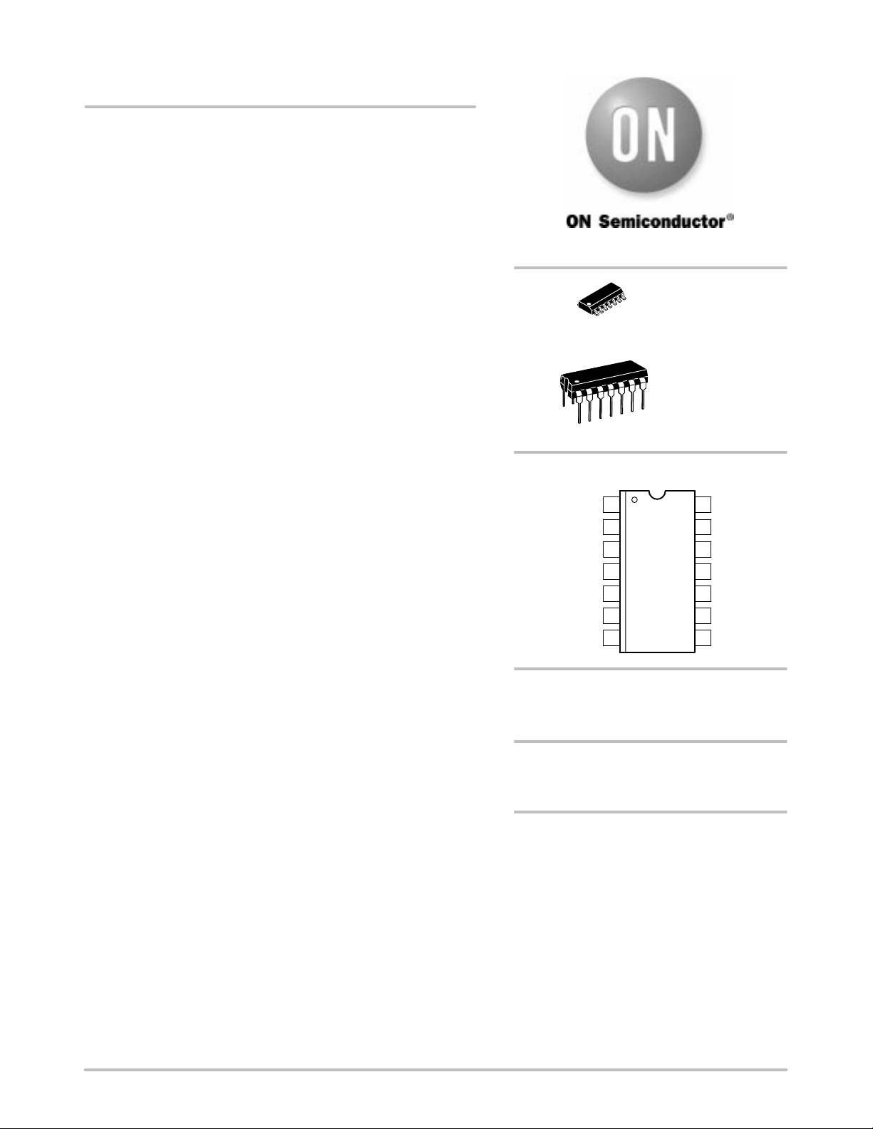
PIN CONNECTIONS
SOIC−14
D SUFFIX
CASE 751A
PDIP−14
P SUFFIX
CASE 646
Signal Input
Gain Adjust
Gain Adjust
Signal Input
Bias
Output
N/C
1
2
3
4
5
6
7
14
V
13
N/C
12
Output
11
N/C
10
Carrier Input
9
N/C
8
Input Carrier
EE
ORDERING INFORMATION
See detailed ordering and shipping information in the package
dimensions section on page 12 of this data sheet.
DEVICE MARKING INFORMATION
See general marking information in the device marking
section on page 12 of this data sheet.
*For additional information on our Pb−Free strategy
and soldering details, please download the ON
Semiconductor Soldering and Mounting Techniques
Reference Manual, SOLDERRM/D.
Semiconductor Components Industries, LLC, 2004
April, 2004 − Rev. 9
1 Publication Order Number:
MC1496/D
Page 2
MC1496, MC1496B
0
20
Log Scale Id
I
= 500 kHz
C
= 1.0 kHz
I
S
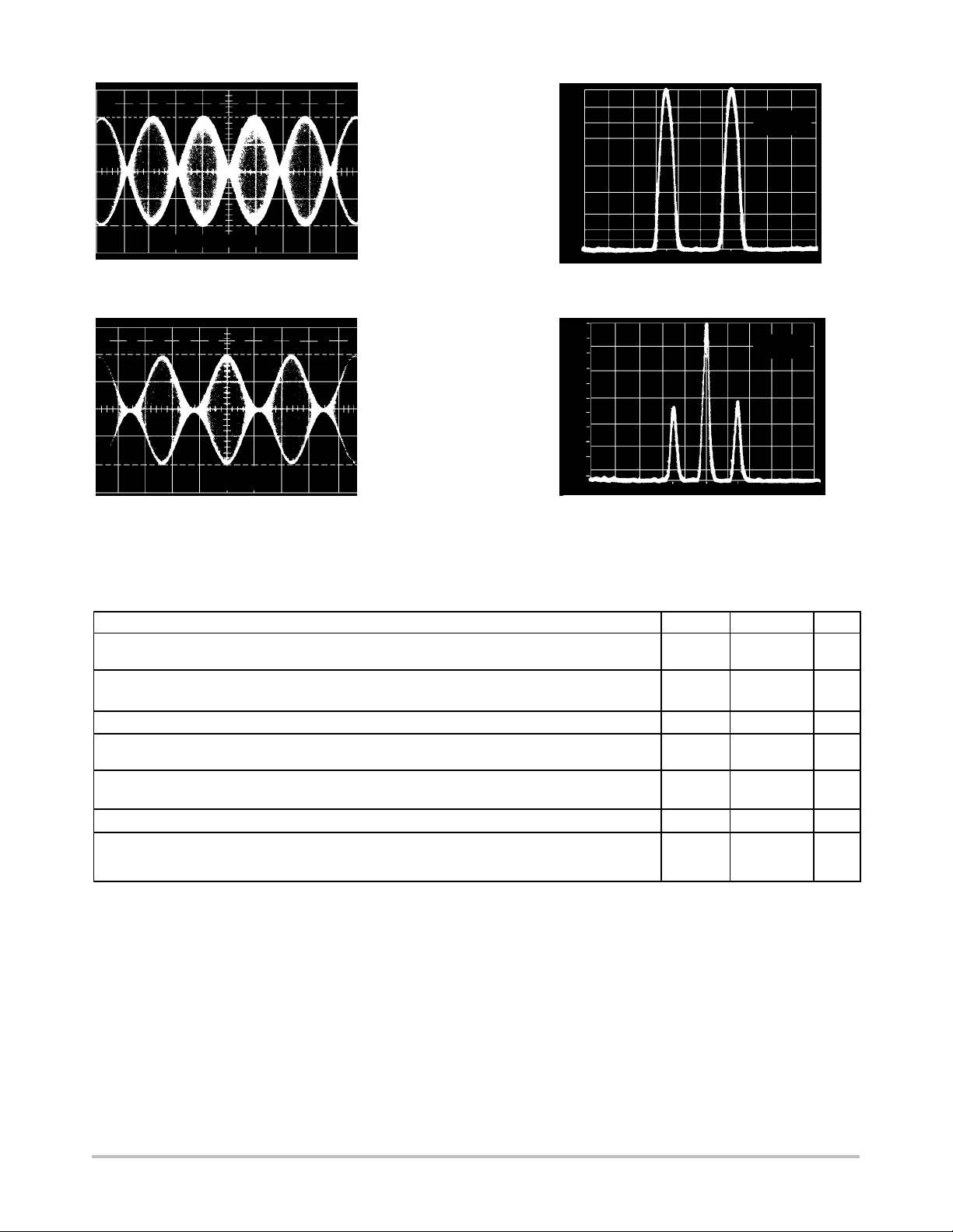
IC = 500 kHz, IS = 1.0 kHz
Figure 1. Suppressed Carrier Output
40
60
499 kHz 500 kHz 501 kHz
Figure 2. Suppressed Carrier Spectrum
Waveform
10
I
= 500 kHz
C
= 1.0 kHz
I
S
= 500 kHz
I
C
= 1.0 kHz
I
S
Figure 3. Amplitude Modulation
8.0
6.0
4.0
Linear Scale
2.0
0
499 kHz 500 kHz 501 kHz
Figure 4. Amplitude−Modulation Spectrum
Output Waveform
MAXIMUM RATINGS
Applied Voltage
(V6−V8, V10−V1, V12−V8, V12−V10, V8−V4, V8−V1, V10−V4, V6−V10, V2−V5, V3−V5)
Differential Input Signal V8 − V10
Maximum Bias Current I
Thermal Resistance, Junction−to−Air
Plastic Dual In−Line Package
Operating Ambient Temperature Range MC1496
Storage Temperature Range T
Electrostatic Discharge Sensitivity (ESD)
Human Body Model (HBM)
Machine Model (MM)
Maximum ratings are those values beyond which device damage can occur. Maximum ratings applied to the device are individual stress limit
values (not normal operating conditions) and are not valid simultaneously . If these limits are exceeded, device functional operation is not implied,
damage may occur and reliability may be affected.
(TA = 25°C, unless otherwise noted.)
Rating
MC1496B
Symbol Value Unit
V 30 Vdc
V4 − V1
5
R
JA
T
A
+5.0
±(5+I5R
10 mA
100 °C/W
0 to +70
Vdc
)
e
°C
−40 to +125
stg
ESD
−65 to +150
°C
V
2000
400
http://onsemi.com
2
Page 3
MC1496, MC1496B
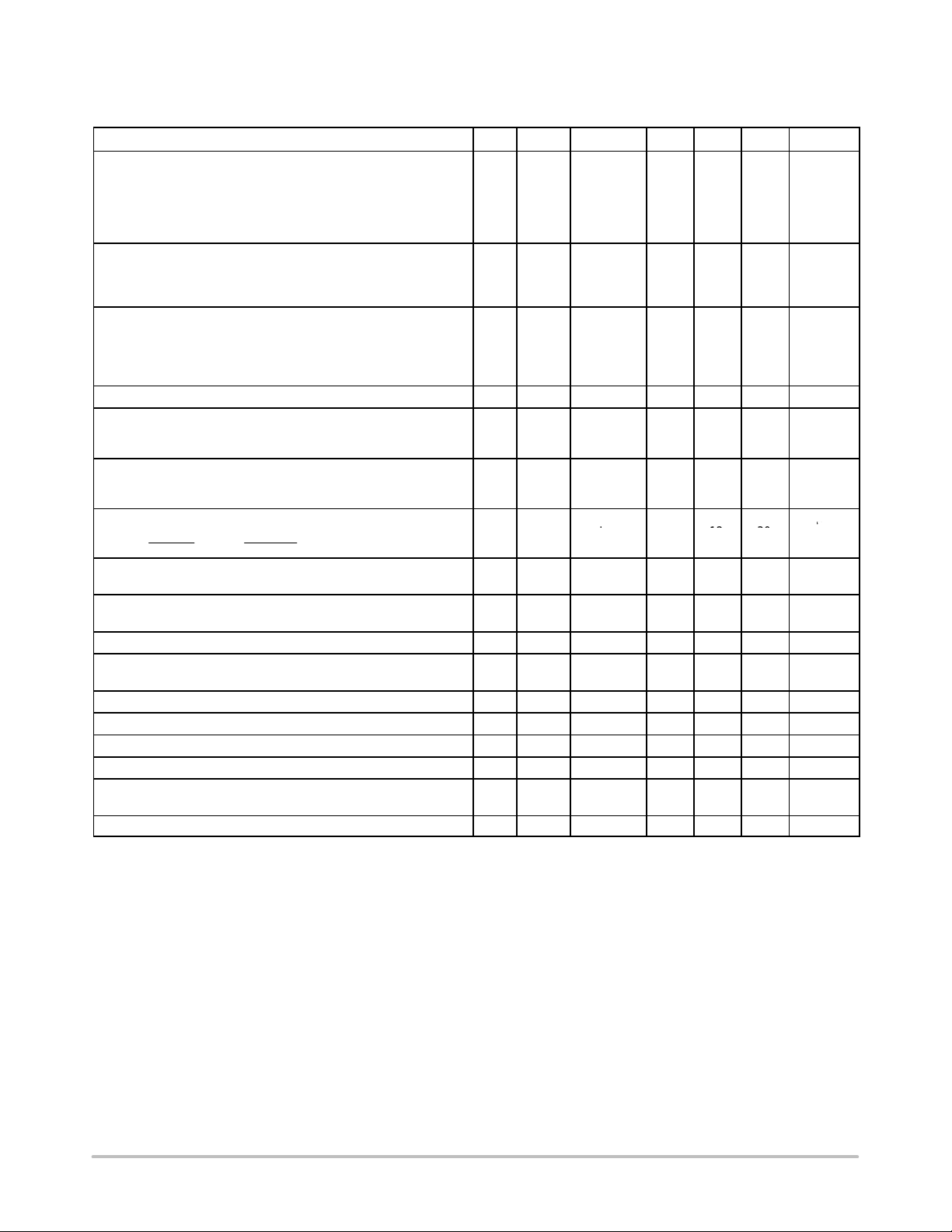
ELECTRICAL CHARACTERISTICS (V
= 12 Vdc, VEE = −8.0 Vdc, I5 = 1.0 mAdc, RL = 3.9 k, Re = 1.0 k, TA = T
CC
low
to T
all input and output characteristics are single−ended, unless otherwise noted.) (Note 1)
Characteristic
Carrier Feedthrough
= 60 mVrms sine wave and
V
C
offset adjusted to zero
= 300 mVpp square wave:
V
C
offset adjusted to zero
offset not adjusted
fC = 1.0 kHz
f
= 10 MHz
C
fC = 1.0 kHz
= 1.0 kHz
f
C
Carrier Suppression
= 10 kHz, 300 mVrms
f
S
f
= 500 kHz, 60 mVrms sine wave
C
= 10 MHz, 60 mVrms sine wave
f
C
Transadmittance Bandwidth (Magnitude) (RL = 50 )
Carrier Input Port, V
= 1.0 kHz, 300 mVrms sine wave
f
S
Signal Input Port, V
| = 0.5 Vdc
|V
C
= 60 mVrms sine wave
C
= 300 mVrms sine wave
S
Signal Gain (VS = 100 mVrms, f = 1.0 kHz; |VC|= 0.5 Vdc) 10 3 A
Single−Ended Input Impedance, Signal Port, f = 5.0 MHz
Parallel Input Resistance
Parallel Input Capacitance
Single−Ended Output Impedance, f = 10 MHz
Parallel Output Resistance
Parallel Output Capacitance
Input Bias Current
I1 I4
I
bS
;I
2
bC
I8 I10
2
Input Offset Current
= I1−I4; I
I
ioS
= I8−I10
ioC
Average Temperature Coefficient of Input Offset Current
(T
= −55°C to +125°C)
A
Fig. Note Symbol Min Typ Max Unit
5 1 V
5 2 V
8 8 BW
CFT
CS
VS
3dB
−
40
40
−
140
−
0.04
−
20
65
−
50
−
300
−
80
−
−
0.4
200
−
−
−
−
2.5 3.5 − V/V
6 −
r
ip
c
ip
−
200
−
2.0
−
−
6 −
r
op
c
oo
−
40
−
5.0
−
−
7 −
I
I
7 − I
I
ioC
7 − TC
bS
bC
ioS
Iio
−
12
−
12
−
0.7
−
0.7
30
30
7.0
7.0
− 2.0 − nA/°C
Output Offset Current (I6−I9) 7 − Ioo − 14 80 A
Average Temperature Coefficient of Output Offset Current
= −55°C to +125°C)
(T
A
7 − TC
− 90 − nA/°C
Ioo
Common−Mode Input Swing, Signal Port, fS = 1.0 kHz 9 4 CMV − 5.0 − Vpp
Common−Mode Gain, Signal Port, fS = 1.0 kHz, |VC|= 0.5 Vdc 9 − ACM − −85 − dB
Common−Mode Quiescent Output Voltage (Pin 6 or Pin 9) 10 − V
Differential Output Voltage Swing Capability 10 − V
Power Supply Current I6 +I12
7 6 I
Power Supply Current I14
DC Power Dissipation 7 5 P
1. T
=0°C for MC1496 T
low
= −40°C for MC1496B = +125°C for MC1496B
= +70°C for MC1496
high
out
out
CC
I
EE
D
− 8.0 − Vpp
− 8.0 − Vpp
−
2.0
−
3.0
4.0
5.0
− 33 − mW
,
high
Vrms
mVrms
dB
k
MHz
k
pF
k
pF
A
A
mAdc
http://onsemi.com
3
Page 4

MC1496, MC1496B
GENERAL OPERATING INFORMATION
Carrier Feedthrough
Carrier feedthrough is defined as the output voltage at
carrier frequency with only the carrier applied
(signal voltage = 0).
Carrier null is achieved by balancing the currents in the
differential amplifier by means of a bias trim potentiometer
(R1 of Figure 5).
Carrier Suppression
Carrier suppression is defined as the ratio of each
sideband output to carrier output for the carrier and signal
voltage levels specified.
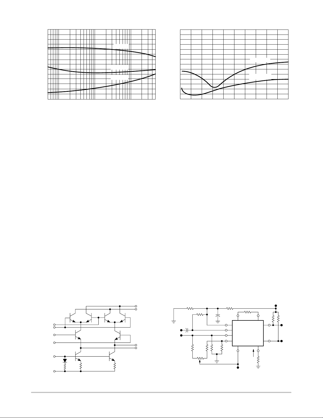
Carrier suppression is very dependent on carrier input
level, as shown in Figure 22. A low value of the carrier does
not fully switch the upper switching devices, and results in
lower signal gain, hence lower carrier suppression. A higher
than optimum carrier level results in unnecessary device and
circuit carrier feedthrough, which again degenerates the
suppression figure. The MC1496 has been characterized
with a 60 mVrms sinewave carrier input signal. This level
provides optimum carrier suppression at carrier frequencies
in the vicinity of 500 kHz, and is generally recommended for
balanced modulator applications.
Carrier feedthrough is independent of signal level, V
Thus carrier suppression can be maximized by operating
with large signal levels. However, a linear operating mode
must be maintained in the signal−input transistor pair − or
harmonics of the modulating signal will be generated and
appear in the device output as spurious sidebands of the
suppressed carrier. This requirement places an upper limit
on input−signal amplitude (see Figure 20). Note also that an
optimum carrier level is recommended in Figure 22 for good
carrier suppression and minimum spurious sideband
generation.
At higher frequencies circuit layout is very important in
order to minimize carrier feedthrough. Shielding may be
necessary in order to prevent capacitive coupling between
the carrier input leads and the output leads.
Signal Gain and Maximum Input Level
Signal gain (single−ended) at low frequencies is defined
as the voltage gain,
R
o
S
L
Re2r
where r
e
e
26 mV
I5(mA)
VS
V
V
A
A constant dc potential is applied to the carrier input
terminals to fully switch two of the upper transistors “on”
and two transistors “off” (VC = 0.5 Vdc). This in effect
forms a cascode differential amplifier.
Linear operation requires that the signal input be below a
critical value determined by R
VS I5 RE (Volts peak)
and the bias current I5.
E
Note that in the test circuit of Figure 10, VS corresponds to
a maximum value of 1.0 V peak.
Common Mode Swing
The common−mode swing is the voltage which may be
applied to both bases of the signal differential amplifier,
without saturating the current sources or without saturating
the differential amplifier itself by swinging it into the upper
switching devices. This swing is variable depending on the
particular circuit and biasing conditions chosen.
Power Dissipation
Power dissipation, PD, within the integrated circuit
package should be calculated as the summation of the
voltage−current products at each port, i.e. assuming
V12 = V6, I5 = I6 = I12 and ignoring base current,
P
=
2 I5 (V6 − V14) + I5)V5 − V14 where subscripts refer
D
to pin numbers.
Design Equations
The following is a partial list of design equations needed
to operate the circuit with other supply voltages and input
conditions.
S
The internal b ias c urrents a re s et b y t he c onditions a t P in 5.
A. Operating Current
.
Assume:
I5 = I6 = I12,
I
IC for all transistors
B
then :
R5
V
I5
500
where: R5 is the resistor between
where: Pin 5 and ground
where: = 0.75 at T
= +25°C
A
The MC1496 has been characterized for the condition
I5 = 1.0 mA and is the generally recommended value.
B. Common−Mode Quiescent Output Voltage
V6 = V12 = V+ − I5 R
Biasing
L
The MC1496 requires three dc bias voltage levels which
must be set externally. Guidelines for setting up these three
levels include maintaining at least 2.0 V collector−base bias
on all transistors while not exceeding the voltages given in
the absolute maximum rating table;
30 Vdc [(V6, V12) − (V8, V10)] 2 Vdc
30 Vdc [(V8, V10) − (V1, V4)] 2.7 Vdc
30 Vdc [(V1, V4) − (V5)] 2.7 Vdc
The foregoing conditions are based on the following
approximations:
V6 = V12, V8 = V10, V1 = V4
http://onsemi.com
4
Page 5
MC1496, MC1496B
s
Bias currents flowing into Pins 1, 4, 8 and 10 are transistor
base currents and can normally be neglected if external bias
dividers are designed to carry 1.0 mA or more.
Transadmittance Bandwidth
Carrier transadmittance b andwidth i s t he 3 .0 d B b andwidth
of the device forward transadmittance as defined by:
21C
vs(signal)
Vo 0
io(each sideband)
Signal transadmittance bandwidth is the 3 .0 d B b andwidth
of the device forward transadmittance as defined by:
io(signal)
21S
v
(signal)
Coupling and Bypass Capacitors
Vc 0.5 Vdc, Vo 0
Capacitors C1 and C2 (Figure 5) should be selected for a
reactance of less than 5.0 at the carrier frequency.
Output Signal
The output signal is taken from Pins 6 and 12 either
balanced or single−ended. Figure 1 1 shows the output levels
of each of the two output sidebands resulting from variations
in both the carrier and modulating signal inputs with a
single−ended output connection.
Negative Supply
VEE should be dc only. The insertion of an RF choke in
series with V
can enhance the stability of the internal
EE
current sources.
Signal Port Stability
Under certain values of driving source impedance,
oscillation may occur. In this event, an RC suppression
network should be connected directly to each input using
short leads. This will reduce the Q of the source−tuned
circuits that cause the oscillation.
Signal Input
(Pins 1 and 4)
510
10 pF
An alternate method for low−frequency applications is to
insert a 1.0 k resistor in series with the input (Pins 1, 4). In
this case input current drift may cause serious degradation
of carrier suppression.
Carrier
Input
V
V
Modulating
Signal Input
C
S
C
2
0.1 F
10 k
1.0 k
R1
51
50 k
Carrier Null
C1
0.1 F
515110 k
1.0 k
8
10
1
4
−8.0 Vdc
1.0 k
2
MC1496
14 5
I10
−
V
V
EE
R
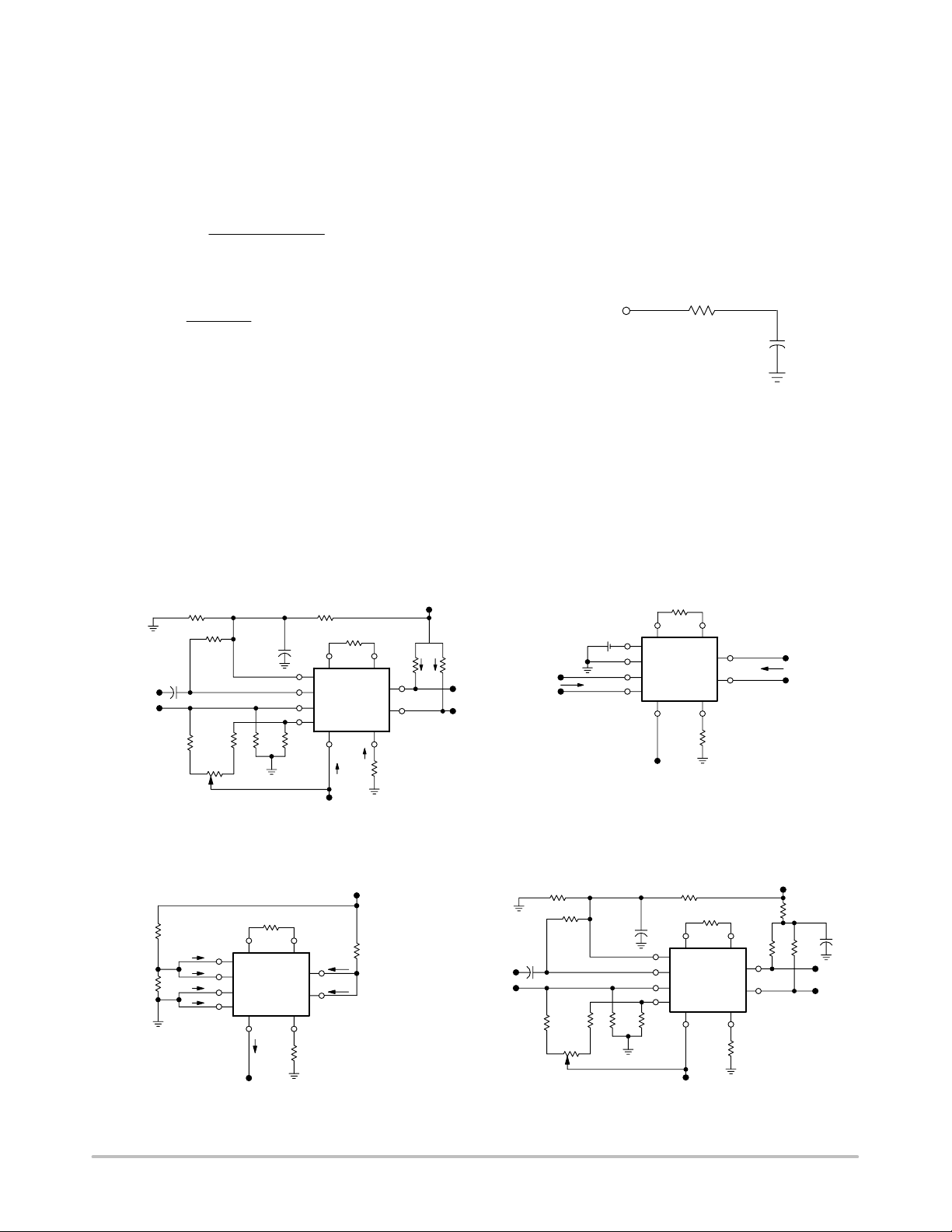
Figure 5. Carrier Rejection and Suppression
V
12 Vdc
R
= 1.0 k
2
8
10
1
4
−8.0 Vdc
V
e
MC1496
14 5
I10
EE
3
6.8 k
I6
6
I9
12
1.0 k
1.0 k
I7
I8
I1
I4
Figure 7. Bias and Offset Currents
e
CC
I5
2.0 k
TEST CIRCUITS
V
CC
12 Vdc
R
L
3
6.8 k
3.9 k
6
12
3.9 k
I6
I9
R
L
+V
o
−V
o
Carrier
Input
Modulating
Signal Input
R
= 1.0 k
e
−
2
8
10
1
4
−8.0 Vdc
MC1496
14 5
0.5 V
+
Z
in
NOTE: Shielding of input and output leads may be needed
to properly perform these tests.
3
6
12
6.8 k
Figure 6. Input−Output Impedance
1.0 k
51
0.1 F
0.1 F
V
C
V
S
10 k
50 k
Carrier Null
51
1.0 k
R
e
1.0 k
23
8
10
MC1496
1
4
14
5110 k
−
V
−8.0 Vdc
V
EE
5
Figure 8. Transconductance Bandwidth
6
12
6.8 k
+V
Z
out
−V
V
12 Vdc
2.0 k
50 50
o
o
CC
0.01
F
+V
o
−V
o
http://onsemi.com
5
Page 6
V
p
1.0 k
S
V , OUTPUT AMPLITUDE OF EACH SIDEBAND (Vrms)
MC1496, MC1496B
V
CC
12 Vdc
R
= 1.0 k
50
1.0 k
0.5 V
+
−
2
8
10
1
4
−8.0 Vdc
e
MC1496
14 5
V
EE
3.9 k
3
6
12
6.8 k
ACM 20 log
3.9 k
+V
−V
o
o
Vo
V
1.0 k
0.5 V
1.0 k
+
V
S
50
S
−
8
10
1
4
−8.0 Vdc
R
e
2
MC1496
14 5
I5 =
1.0 mA
V
EE
= 1.0 k
3
6.8 k
3.9 k
6
12
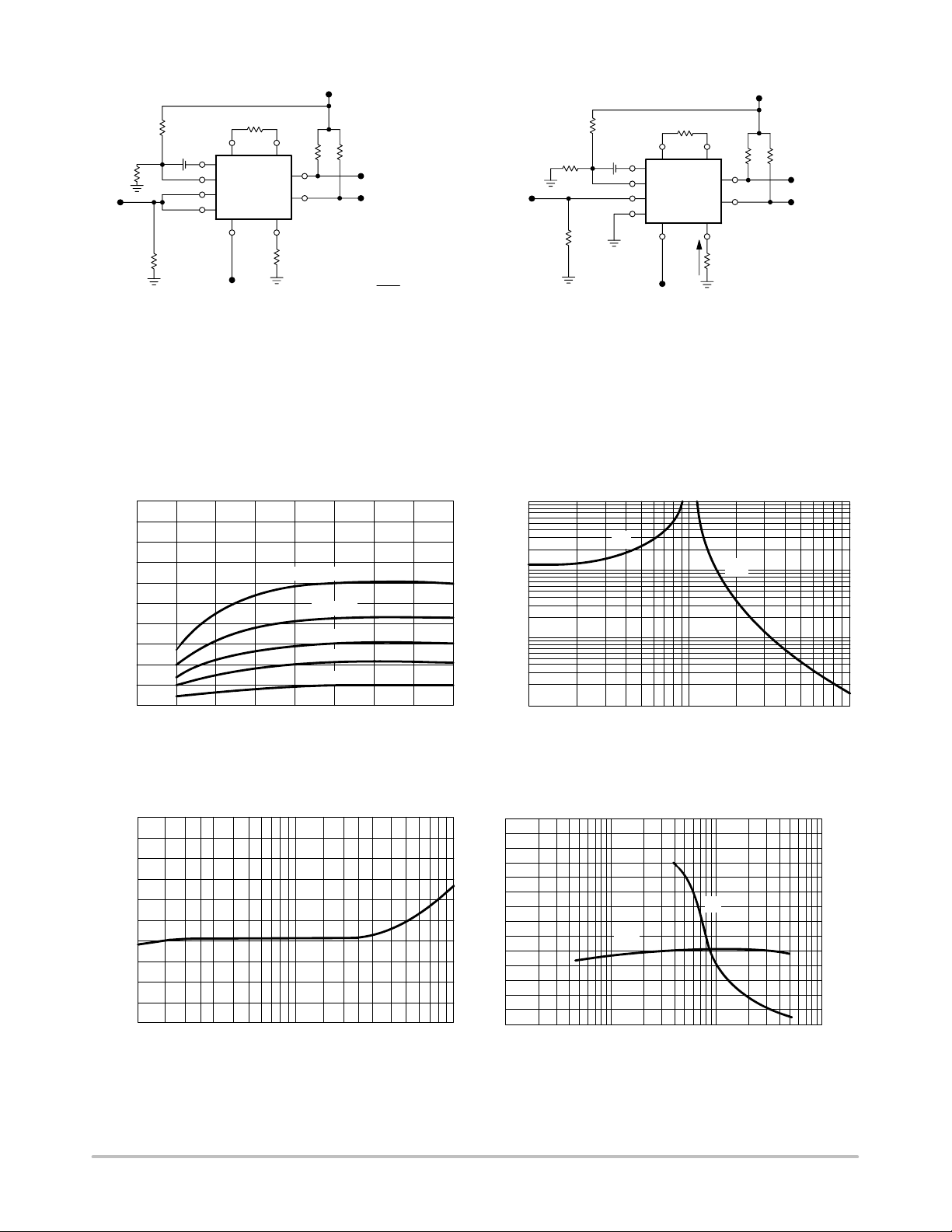
Figure 9. Common Mode Gain Figure 10. Signal Gain and Output Swing
TYPICAL CHARACTERISTICS
Typical characteristics were obtained with circuit shown in Figure 5, fC = 500 kHz (sine wave),
V
= 60 mVrms, fS = 1.0 kHz, VS = 300 mVrms, TA = 25°C, unless otherwise noted.
C
2.0
1.6
1.2
Signal Input = 600 mV
400 mV
0.8
0.4
0
O
0
V
, CARRIER LEVEL (mVrms)
C
300 mV
200 mV
100 mV
10050 150
200
Figure 11. Sideband Output versus
Carrier Levels
1.0 M
Ω)
500
100
50
10
5.0
ip
1.0
r , PARALLEL INPUT RESISTANCE (k
+r
ip
−r
1.0
5.0 100
10
f, FREQUENCY (MHz)
Figure 12. Signal−Port Parallel−Equivalent
Input Resistance versus Frequency
V
CC
12 Vdc
3.9 k
+V
o
−V
o
ip
50
5.0
4.0
3.0
2.0
1.0
ip
c , PARALLEL INPUT CAPACITANCE (pF)
0
1.0
5.0
5020
Figure 13. Signal−Port Parallel−Equivalent
Input Capacitance versus Frequency
http://onsemi.com
140
14
Ω)
120
100
r
80
60
c
op
op
40
20
0
op
r , PARALLEL OUTPUT RESISTANCE (k
100102.0
0
1.0
12
10
8.0
6.0
4.0
2.0
o
c , PARALLEL OUTPUT CAPACITANCE (pF)
0
10010
f, FREQUENCY (MHz)f, FREQUENCY (MHz)
Figure 14. Single−Ended Output Impedance
versus Frequency
6
Page 7
MC1496, MC1496B
TYPICAL CHARACTERISTICS (continued)
Typical characteristics were obtained with circuit shown in Figure 5, fC = 500 kHz (sine wave),
V
= 60 mVrms, fS = 1.0 kHz, VS = 300 mVrms, TA = 25°C, unless otherwise noted.
C
1.0
0.9
0.8
0.7
0.6
0.5
0.4
0.3
0.2
21, TRANSADMITTANCE (mmho)
γ
0.1
0
0.1
20
10
0
−10
−20
S
V
A , SINGLE-ENDED VOLTAGE GAIN (dB)
−30
0
Signal Port
Side Band
Sideband Transadmittance
I
(EachSideband)
out
21
21
Vin(Signal)
Signal Port Transadmittance
I
out
V
0|VC| 0.5Vdc
out
V
in
fC, CARRIER FREQUENCY (MHz)
V
0
out
10
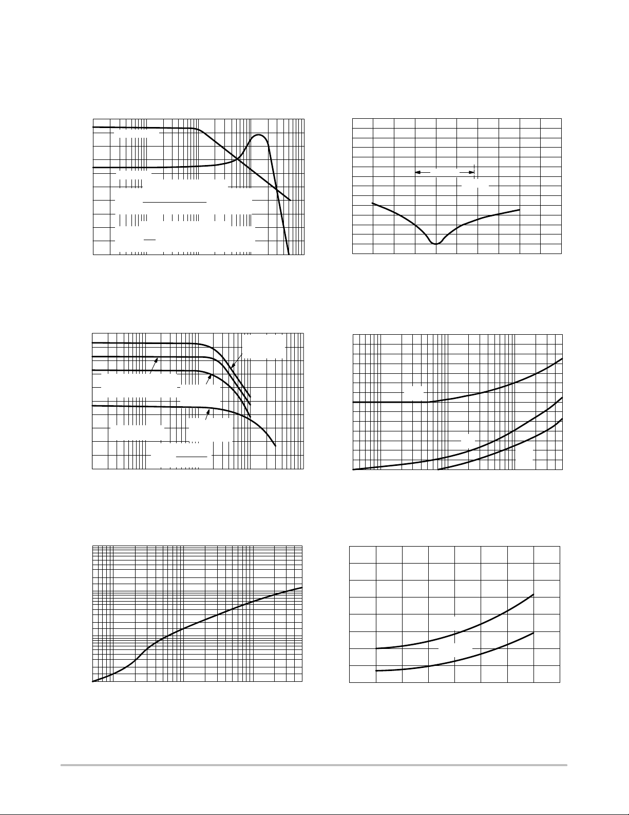
Figure 15. Sideband and Signal Port
Transadmittances versus Frequency
RL = 3.9 k (Standard
Re = 1.0 k Test Circuit)
|VC| = 0.5 Vdc
0.1 1.0 10 1000.01
RL = 3.9 k
Re = 2.0 k
RL = 500
Re = 1.0 k
R
AV
L
Re 2r
e
f, FREQUENCY (MHz)
1001.0
RL = 3.9 k
Re = 500
1000
10
20
30
40
50
CS
60
V , CARRIER SUPPRESION (dB)
70
−75 −50
T
, AMBIENT TEMPERATURE (°C)
A
Figure 16. Carrier Suppression
versus Temperature
0
10
20
30
40
50
CARRIER SIDEBAND (dB)
60
70
SUPPRESSION BELOW EACH FUNDAMENTAL
2f
C
fC, CARRIER FREQUENCY (MHz)
MC1496
(70°C)
100 125 150 175
7550250−25
f
C
3f
Figure 17. Signal−Port Frequency Response Figure 18. Carrier Suppression
versus Frequency
C
505.00.05 0.1 0.5 1.0 10
CFT
V , CARRIER OUTPUT VOLTAGE (mVrms)
1.0
0.1
0.01
10
1.0 5.00.05 0.1 0.5
f
, CARRIER FREQUENCY (MHz)
C
5010
Figure 19. Carrier Feedthrough
versus Frequency
0
10
20
30
40
50
60
CARRIER SIDEBAND (dB)
70
80
SUPPRESSION BELOW EACH FUNDAMENTAL
0
Figure 20. Sideband Harmonic Suppression
f
± 3f
C
S
f
± 2f
C
S
V
, INPUT SIGNAL AMPLITUDE (mVrms)
S
versus Input Signal Level
800600400200
http://onsemi.com
7
Page 8
MC1496, MC1496B
0
10
3f
± f
C
20
30
40
50
CARRIER SIDEBAND (dB)
60
70
SUPPRESSION BELOW EACH FUNDAMENTAL
fC, CARRIER FREQUENCY (MHz)
S
2f
± f
C
S
2f
± 2f
C
S
Figure 21. Suppression of Carrier Harmonic
Sidebands versus Carrier Frequency
OPERATIONS INFORMATION
The MC1496, a monolithic balanced modulator circuit, is
shown in Figure 23.
This circuit consists o f a n u pper q uad d ifferential a mplifier
driven by a standard differential amplifier with dual current
sources. The output collectors are cross−coupled so that
full−wave balanced multiplication of the two input voltages
occurs. That is, the output signal is a constant times the
product of the two input signals.
Mathematical analysis of linear ac signal multiplication
indicates that t he o utput s pectrum w ill c onsist o f o nly t he s um
and difference of the two i nput f requencies. T hus, t he d e vice
may be u sed a s a balanced m odulator , d oubly b alanced m ixer ,
product detector, frequency doubler, and other applications
requiring these particular output signal characteristics.
The lower differential amplifier has its emitters connected
to the package pins so that an external emitter resistance may
be used. Also, external load resistors are employed at the
device output.
Signal Levels
The upper quad differential amplifier may be operated
either in a linear or a saturated mode. The lower differential
amplifier is operated in a linear mode for most applications.
For low−level operation at both input ports, the output
signal will contain sum and difference frequency
(−) 12
,
V
o
Output
(+) 6
Input
Input
Bias
10 (−)
V
C
8 (+)
4 (−)
V
S
1 (+)
5
500500 500
14V
EE
2
Gain
Adjust
3
(Pin numbers
per G package)
Figure 23. Circuit Schematic Figure 24. Typical Modulator Circuit
Carrier
Signal
0
10
20
30
40
50
60
CS
V , CARRIER SUPPRESSION (dB)
50101.0 5.00.05 0.1 0.5
70
V
, CARRIER INPUT LEVEL (mVrms)
C
fC = 10 MHz
fC = 500 kHz
Figure 22. Carrier Suppression versus
Carrier Input Level
components and have an amplitude which is a function of the
product of the input signal amplitudes.
For high−level operation at the carrier input port and
linear operation at the modulating signal port, the output
signal will contain sum and difference frequency
components of the modulating signal frequency and the
fundamental and odd harmonics of the carrier frequency.
The output amplitude will be a constant times the
modulating signal amplitude. Any amplitude variations in
the carrier signal will not appear in the output.
The linear signal handling capabilities of a differential
amplifier are well defined. With no emitter degeneration, the
maximum input voltage for linear operation is
approximately 25 mV peak. Since the upper differential
amplifier has its emitters internally connected, this voltage
applies to the carrier input port for all conditions.
Since the lower differential amplifier has provisions for an
external emitter resistance, its linear signal handling range
may be adjusted by the user. The maximum input voltage for
linear operation may be approximated from the following
expression:
V = (I5) (RE) volts peak.
This expression may be used to compute the minimum
value of R
V
Carrier
Input
V
Modulating
Signal
Input
for a given input voltage amplitude.
E
1.0 k1.0 k
0.1 F
2
8
10
1
4
V
C
S
0.1 F
10 k
51
10 k
50 k
Carrier Null
51351
R
1.0 k
e
MC1496
14
−8.0 Vdc
EE
I5
5
6.8 k
3.9 k
6
12
500100 4003000 200
12 Vdc
R
R
L
L
3.9 k
+V
o
−V
o
http://onsemi.com
8
Page 9
MC1496, MC1496B
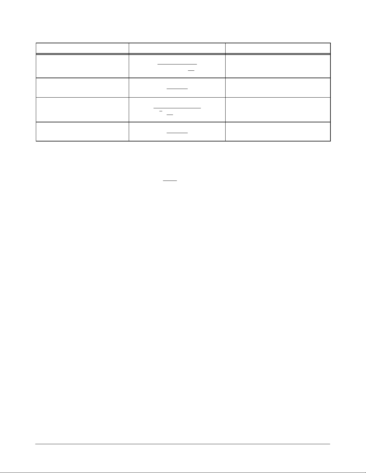
Table 1. Voltage Gain and Output Frequencies
Carrier Input Signal (VC) Approximate Voltage Gain Output Signal Frequency(s)
RLV
Low−level dc
High−level dc
Low−level ac
High−level ac
2. Low−level Modulating Signal, VM, assumed in all cases. VC is Carrier Input Voltage.
3. When the output signal contains multiple frequencies, the gain expression given is for the output amplitude ofeach of the two desired outputs,
+ fM and fC − fM.
f
C
4. All gain expressions are for a single−ended output. For a differential output connection, multiply each expression by two.
5. RL = Load resistance.
= Emitter resistance between Pins 2 and 3.
6. R
E
7. r
= Transistor dynamic emitter resistance, at 25°C;
e
8. K = Boltzmann′s Constant, T = temperature in degrees Kelvin, q = the charge on an electron.
2(RE 2re)
22
re
I5(mA)
C
R
L
RE 2r
RLVC(rms)
KT
RE 2r
26 mV
(RE 2re)
q
0.637 R
e
L
e
f
f
± fM, 5f
C
C
M
f
M
± f
M
± fM, . . .
C
KT
q
f
± fM, 3f
C
The gain from the modulating signal input port to the
output is the MC1496 gain parameter which is most often of
interest to the designer. This gain has significance only when
the lower differential amplifier is operated in a linear mode,
but this includes most applications of the device.
As previously mentioned, the upper quad differential
amplifier may be operated either in a linear or a saturated
mode. Approximate gain expressions have been developed
for the MC1496 for a low−level modulating signal input and
the following carrier input conditions:
1) Low−level dc
2) High−level dc
3) Low−level ac
4) High−level ac
These gains are summarized in Table 1, along with the
frequency components contained in the output signal.
APPLICATIONS INFORMATION
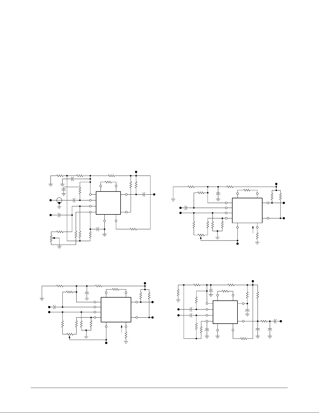
Double sideband suppressed carrier modulation is the
basic application of the MC1496. The suggested circuit for
this application is shown on the front page of this data sheet.
In some applications, it may be necessary to operate the
MC1496 with a single dc supply voltage instead of dual
supplies. Figure 25 shows a balanced modulator designed
for operation with a single 12 Vdc supply. Performance of
this circuit is similar to that of the dual supply modulator.
AM Modulator
The circuit shown in Figure 26 may be used as an
amplitude modulator with a minor modification.
All that is required to shift from suppressed carrier to AM
operation is to adjust the carrier null potentiometer for the
proper amount of carrier insertion in the output signal.
However, the suppressed carrier null circuitry as shown in
Figure 26 does not have sufficient adjustment range.
Therefore, the modulator may be modified for AM
operation by changing two resistor values in the null circuit
as shown in Figure 27.
Product Detector
The MC1496 makes an excellent SSB product detector
(see Figure 28).
This product detector has a sensitivity of 3.0 V and a
dynamic range of 90 dB when operating at an intermediate
frequency of 9.0 MHz.
The detector is broadband for the entire high frequency
range. For operation at very low intermediate frequencies
down to 5 0 kHz the 0.1 F capacitors on Pins 8 and 10 should
be increased to 1.0 F. Also, the output filter at Pin 12 can
be tailored to a specific intermediate frequency and audio
amplifier input impedance.
As in all applications of the MC1496, the emitter
resistance between Pins 2 and 3 may be increased or
decreased to adjust circuit gain, sensitivity, and dynamic
range.
This circuit may also be used as an AM detector by
introducing carrier signal at the carrier input and an AM
signal at the SSB input.
The carrier signal may be derived from the intermediate
frequency signal or generated locally. The carrier signal may
http://onsemi.com
9
Page 10
MC1496, MC1496B
d
−
+
F
p
0
be introduced with or without modulation, provided its level
is sufficiently high to saturate the upper quad differential
amplifier. If the carrier signal is modulated, a 300 mVrms
input level is recommended.
Doubly Balanced Mixer
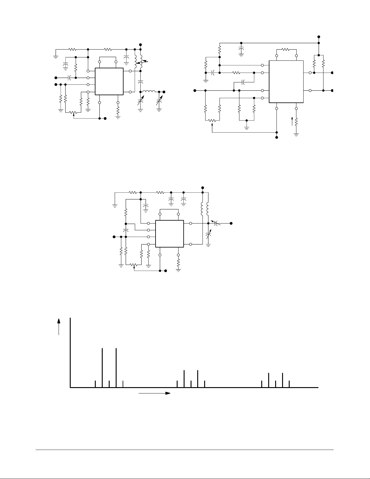
The MC1496 may be used as a doubly balanced mixer
with either broadband or tuned narrow band input and output
networks.
The local oscillator signal is introduced at the carrier input
port with a recommended amplitude of 100 mVrms.
Figure 29 shows a mixer with a broadband input and a
tuned output.
Frequency Doubler
The MC1496 will operate as a frequency doubler by
introducing the same frequency at both input ports.
TYPICAL APPLICATIONS
V
1.0 k
1.3 k820
CC
12 Vdc
Figures 30 and 31 show a broadband frequency doubler
and a tuned output very high frequency (VHF) doubler,
respectively.
Phase Detection and FM Detection
The MC1496 will function as a phase detector. High−level
input signals are introduced at both inputs. When both inputs
are at the same frequency the MC1496 will deliver an output
which is a function of the phase difference between the two
input signals.
An FM detector may be constructed by using the phase
detector principle. A tuned circuit is added at one of the
inputs to cause the two input signals to vary in phase as a
function of frequency. The MC1496 will then provide an
output which is a function of the input signal frequency.
Carrier Input
60 mVrms
Modulating
Signal Input
300 mVrms
Carrier
Null
50 k
V
C
Carrier
Input
V
S
Modulating
Signal
Input
25 F
15 V
−R1+
0.1 F
0.1 F
+
0.1 F
10 F
15 V
10 k 100 100
10 k
51
8
10
1
4
25 F
15 V
+
1.0 k
2
MC1496
−
Figure 25. Balanced Modulator
(12 Vdc Single Supply)
1.0 k1.0 k
0.1 F
51
750 51 51750
50 k
Carrier Adjust
23
8
10
1
4
14 5
14 5
R
1.0 k
e
MC1496
V
EE
−8.0 Vdc
3.0 k 3.0 k
3
6
12
10 k
3.9 k
6
12
6.8 k
15
R
0.1 F
L
DSB
Output
V
CC
12 Vdc
R
3.9 k
+V
−V
L
Carrier Input
o
300 mVrms
SSB Input
o
1.0 k1.0 k
1.0 k
R
e
2
8
10
1
MC1496
4
14 5
V
EE
−8.0 Vdc
V
Carrier
Input
V
Modulating
Signal
Input
C
S
0.1 F
51
10 k10 k 51 51
50 k
Carrier Null
0.1 F
Figure 26. Balanced Modulator−Demodulator
1.3 k820
0.1 F
1.0 k
0.1 F
0.1 F
1.0 k
51
1.0 k
8
10
1
4
0.1
F
100
2
MC1496
14 5
3.0 k 3.0 k
3
6
12
10 k
I5
3
6.8 k
V
CC
12 Vdc
0.005
F
0.005
F
3.9 k
12
1.0 k
V
CC
12 V
R
L
R
L
3.9
6
A
1.0 F
Out
RL 1
0.005
F
Figure 27. AM Modulator Circuit Figure 28. Product Detector
(12 Vdc Single Supply)
http://onsemi.com
10
Page 11
1.0 k
c
k
p
0.001 F
Local
Oscillator
Input
100 mVrms
51
0.001 F
RF Input
10 k
51
10 k 51
50 k
Null Adjust
L1 = 44 Turns AWG No. 28 Enameled Wire, Wound
on Micrometals Type 44−6 Toroid Core.
8
10
1
4
1.0 k
2
MC1496
14
0.01
F
3
V
EE
−8.0 Vdc
6
12
5
5.0−80
6.8 k
Figure 29. Doubly Balanced Mixer
(Broadband Inputs, 9.0 MHz Tuned Output)
100
0.001 F
150 MHz
Input
100
pF
10 k
10 k
50 k
Balance
MC1496, MC1496B
V
CC
+8.0 Vdc
RFC
100 H
0.001 F
9.5 F
L1
1.0 k1.0 k
0.001
F
8
10
1
4
100
9.0 MHz
Output
R
L
90−480 pF
0.001
F
23
MC1496
14 5
V
EE
−8.0 Vdc
Input
15 mVrms
= 50
18 pF
0.68 H
6
12
6.8 k
1.0 k
C2
100 F
15 Vdc Max
10 k 10 k
50 k
Balance
V
CC
+
+8.0 Vdc
V
L1
R
FC
18 nH
1.0−10 pF
1.0−10 pF
L1 = 1 Turn AWG
No. 18 Wire, 7/32″ ID
+
1.0 k
100 F
−
25 Vdc
100
C2
+−
100 F 15 Vdc
100
100
10
8
1
4
2
14
1.0 k
MC1496
3.9 k
3
6
12
5
6.8 k
I5
V
EE
−8.0 Vdc
Figure 30. Low−Frequency Doubler
300 MHz
Output
= 50
R
L
V
CC
12 Vd
3.9
Out
AMPLITUDE
C S
C S
(f − f )
(f + f )
C
C S
(f )
(f − 2f )
(f + 2f )
Frequency Balanced Modulator Spectrum
f
Carrier Fundamental
C
Modulating Signal
f
S
Fundamental Carrier Sidebands
fC ± f
S
Figure 31. 150 to 300 MHz Doubler
C S
(2f − 2f )
C S
C S
(2f − 2f )
(2f )
DEFINITIONS
http://onsemi.com
11
C S
(2f + 2f )
C
fC ± nf
nf
C
nfC ± nf
C S
C S
(2f + 2f )
Fundamental Carrier Sideband Harmonics
S
Carrier Harmonics
Carrier Harmonic Sidebands
S
(3f − f )
C S
(3f − 2f )
C
(3f )
C S
(3f + f )
C S
(3f + 2f )
Page 12
MC1496, MC1496B
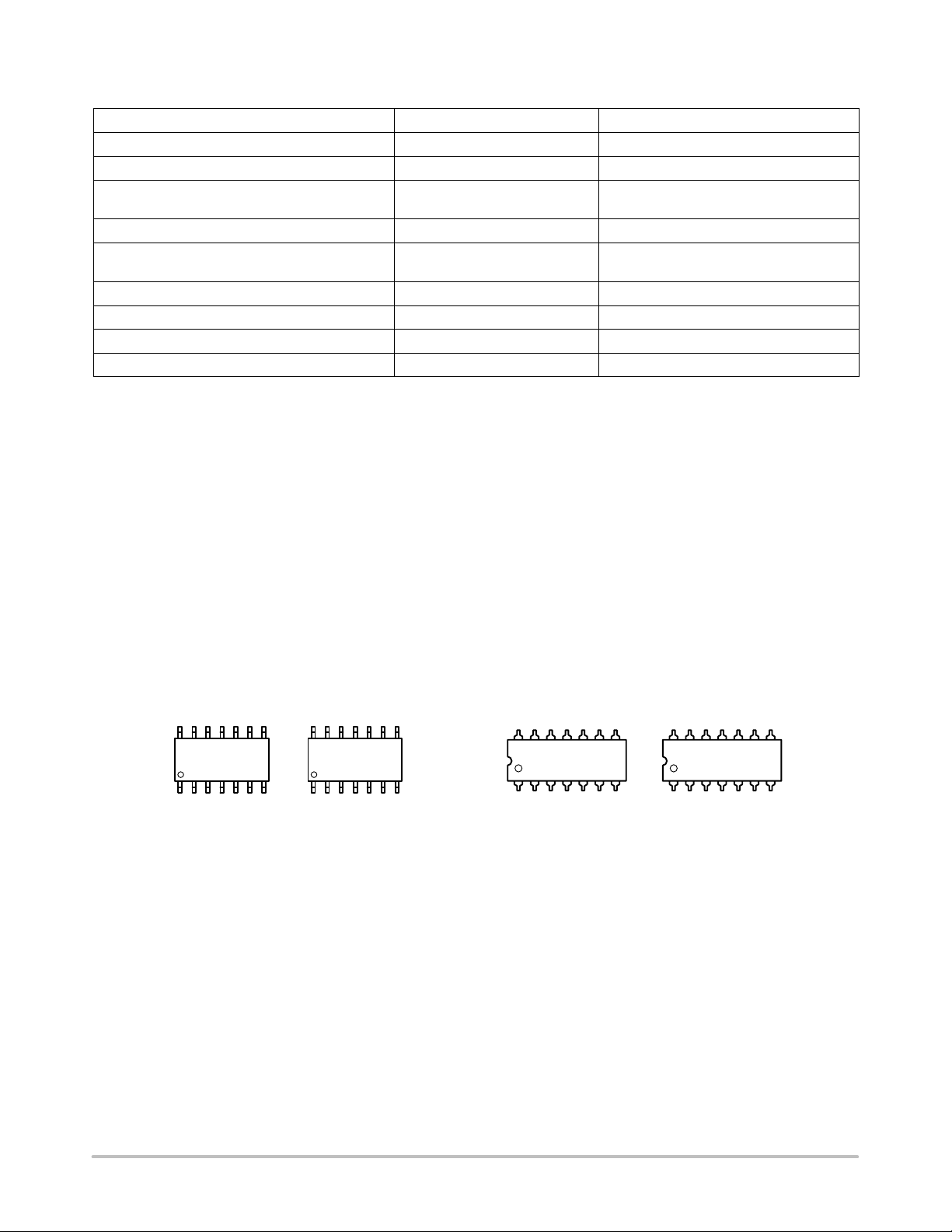
ORDERING INFORMATION
Device Package Shipping
MC1496D SOIC−14 55 Units/Rail
MC1496DR2 SOIC−14 2500 Tape & Reel
MC1496DR2G SOIC−14
(Pb−Free)
MC1496P PDIP−14 25 Units/Rail
MC1496PG PDIP−14
(Pb−Free)
MC1496P1 PDIP−14 25 Units/Rail
MC1496BD SOIC−14 55 Units/Rail
MC1496BDR2 SOIC−14 2500 Tape & Reel
MC1496BP PDIP−14 25 Units/Rail
†For information on tape and reel specifications, including part orientation and tape sizes, please refer to our Tape and Reel Packaging
Specifications Brochure, BRD8011/D.
2500 Tape & Reel
25 Units/Rail
†
14
MC1496D
AWLYWW
1
SOIC−14
D SUFFIX
CASE 751A
14
1
MC1496BD
AWLYWW
MARKING DIAGRAMS
14
1
A = Assembly Location
WL = Wafer Lot
YY, Y = Year
WW = Work Week
MC1496P
AWLYYWW
PDIP−14
P SUFFIX
CASE 646
14
MC1496BP
AWLYYWW
1
http://onsemi.com
12
Page 13
−T−
SEATING
PLANE
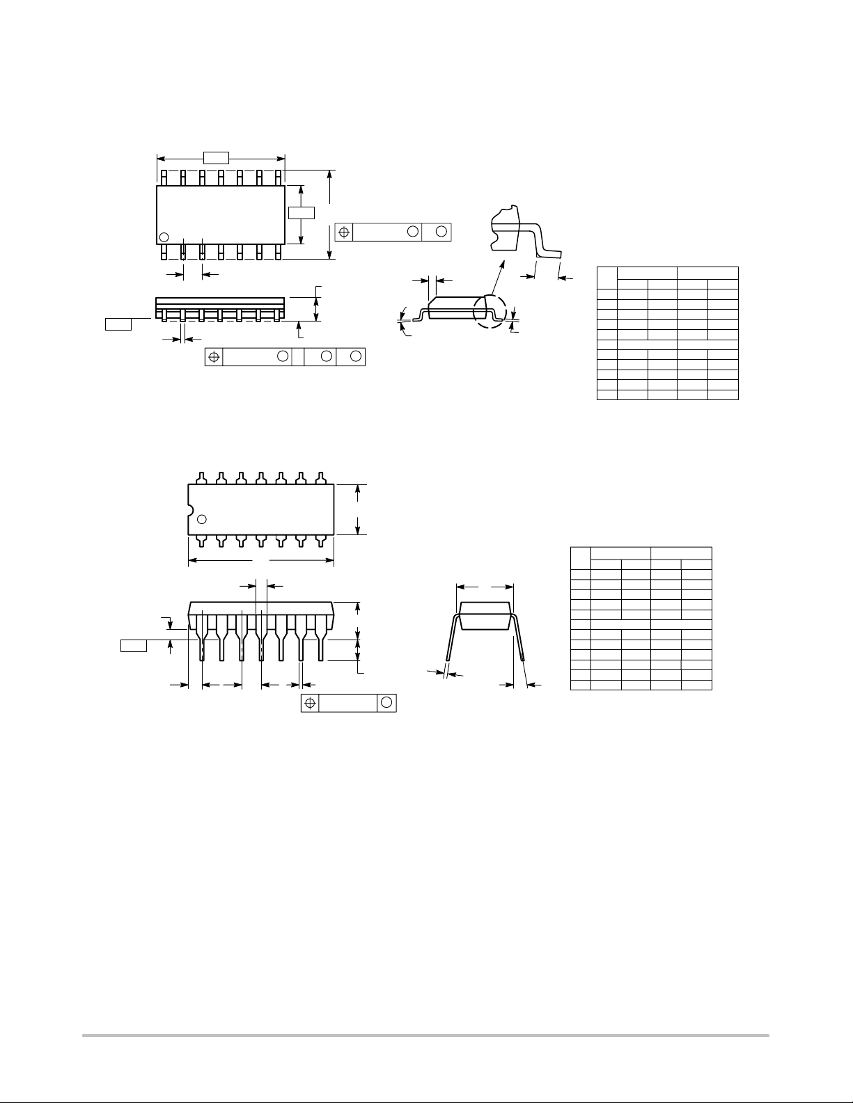
PACKAGE DIMENSIONS
−A−
14 8
−B−
71
G
D 14 PL
0.25 (0.010) A
14 8
17
M
7 PL
P
C
K
S
B
T
MC1496, MC1496B
SOIC−14
D SUFFIX
PLASTIC PACKAGE
CASE 751A−03
ISSUE F
M
0.25 (0.010) B
X 45
R
S
P SUFFIX
PLASTIC PACKAGE
CASE 646−06
B
M
M
PDIP−8
ISSUE M
NOTES:
1. DIMENSIONING AND TOLERANCING PER ANSI
Y14.5M, 1982.
2. CONTROLLING DIMENSION: MILLIMETER.
3. DIMENSIONS A AND B DO NOT INCLUDE
MOLD PROTRUSION.
4. MAXIMUM MOLD PROTRUSION 0.15 (0.006)
PER SIDE.
5. DIMENSION D DOES NOT INCLUDE DAMBAR
PROTRUSION. ALLOWABLE DAMBAR
PROTRUSION SHALL BE 0.127 (0.005) TOTAL
IN EXCESS OF THE D DIMENSION AT
MAXIMUM MATERIAL CONDITION.
F
J
NOTES:
DIM MIN MAX MIN MAX
A 8.55 8.75 0.337 0.344
B 3.80 4.00 0.150 0.157
C 1.35 1.75 0.054 0.068
D 0.35 0.49 0.014 0.019
F 0.40 1.25 0.016 0.049
G 1.27 BSC 0.050 BSC
J 0.19 0.25 0.008 0.009
K 0.10 0.25 0.004 0.009
M 0 7 0 7
P 5.80 6.20 0.228 0.244
R 0.25 0.50 0.010 0.019
1. DIMENSIONING AND TOLERANCING PER ANSI
Y14.5M, 1982.
2. CONTROLLING DIMENSION: INCH.
3. DIMENSION L TO CENTER OF LEADS WHEN
FORMED PARALLEL.
4. DIMENSION B DOES NOT INCLUDE MOLD FLASH.
5. ROUNDED CORNERS OPTIONAL.
INCHESMILLIMETERS
−T−
SEATING
PLANE
N
HG
A
F
L
C
D
14 PL
0.13 (0.005)
K
J
M
M
DIM MIN MAX MIN MAX
A 0.715 0.770 18.16 18.80
B 0.240 0.260 6.10 6.60
C 0.145 0.185 3.69 4.69
D 0.015 0.021 0.38 0.53
F 0.040 0.070 1.02 1.78
G 0.100 BSC 2.54 BSC
H 0.052 0.095 1.32 2.41
J 0.008 0.015 0.20 0.38
K 0.115 0.135 2.92 3.43
L
0.290 0.310 7.37 7.87
M −−− 10 −−− 10
N 0.015 0.039 0.38 1.01
MILLIMETERSINCHES
http://onsemi.com
13
Page 14

MC1496, MC1496B
ON Semiconductor and are registered trademarks of Semiconductor Components Industries, LLC (SCILLC). SCILLC reserves the right to make changes without further notice
to any products herein. SCILLC makes no warranty, representation or guarantee regarding the suitability of its products for any particular purpose, nor does SCILLC assume any liability
arising out of the application or use of any product or circuit, and specifically disclaims any and all liability, including without limitation special, consequential or incidental damages.
“Typical” parameters which may be provided in SCILLC data sheets and/or specifications can and do vary in different applications and actual performance may vary over time. All
operating parameters, including “Typicals” must be validated for each customer application by customer’s technical experts. SCILLC does not convey any license under its patent rights
nor the rights of others. SCILLC products are not designed, intended, or authorized for use as components in systems intended for surgical implant into the body, or other applications
intended to support or sustain life, or for any other application in which the failure of the SCILLC product could create a situation where personal injury or death may occur. Should
Buyer purchase or use SCILLC products for any such unintended or unauthorized application, Buyer shall indemnify and hold SCILLC and its officers, employees, subsidiaries, affiliates,
and distributors harmless against all claims, costs, damages, and expenses, and reasonable attorney fees arising out of, directly or indirectly, any claim of personal injury or death
associated with such unintended or unauthorized use, even if such claim alleges that SCILLC was negligent regarding the design or manufacture of the part. SCILLC is an Equal
Opportunity/Affirmative Action Employer. This literature is subject to all applicable copyright laws and is not for resale in any manner.
PUBLICATION ORDERING INFORMATION
LITERATURE FULFILLMENT:
Literature Distribution Center for ON Semiconductor
P.O. Box 5163, Denver, Colorado 80217 USA
Phone: 303−675−2175 or 800−344−3860 Toll Free USA/Canada
Fax: 303−675−2176 or 800−344−3867 Toll Free USA/Canada
Email: [email protected]
N. American Technical Support: 800−282−9855 Toll Free
USA/Canada
Japan: ON Semiconductor, Japan Customer Focus Center
2−9−1 Kamimeguro, Meguro−ku, Tokyo, Japan 153−0051
Phone: 81−3−5773−3850
http://onsemi.com
ON Semiconductor Website: http://onsemi.com
Order Literature: http://www.onsemi.com/litorder
For additional information, please contact your
local Sales Representative.
MC1496/D
14
 Loading...