

Page 1
Order this document by MC1495/D
The MC1495 is designed for use where the output is a linear product of
two input voltages. Maximum versatility is assured by allowing the user to
select the level shift method. Typical applications include: multiply, divide*,
square root*, mean square*, phase detector, frequency doubler, balanced
modulator/demodulator, and electronic gain control.
• Wide Bandwidth
• Excellent Linearity:
2% max Error on X Input, 4% max Error on Y Input Over Temperature
1% max Error on X Input, 2% max Error on Y Input at + 25°C
• Adjustable Scale Factor, K
• Excellent Temperature Stability
• Wide Input Voltage Range: ± 10 V
• ±15 V Operation
*When used with an operational amplifier.
LINEAR
FOUR-QUADRANT
MUL TIPLIER
SEMICONDUCTOR
TECHNICAL DATA
14
1
D SUFFIX
PLASTIC PACKAGE
CASE 751A
(SO-14)
MAXIMUM RATINGS (T
Rating Symbol Value Unit
Applied Voltage
(V2–V1, V14–V1, V1–V9, V1–V12, V1–V4,
V1–V8, V12–V7, V9–V7, V8–V7, V4–V7)
Differential Input Signal V12–V
Maximum Bias Current I
Operating Temperature Range
Storage Temperature Range T
= + 25°C, unless otherwise noted.)
A
V4–V
MC1495
MC1495B
MOTOROLA ANALOG IC DEVICE DATA
∆V 30 Vdc
I
T
3
13
A
stg
± (6+I13 RX)
9
± (6+I3 RY)
8
10
10
0 to +70
– 40 to +125
– 65 to +150 °C
Vdc
mA
°C
14
1
P SUFFIX
PLASTIC PACKAGE
CASE 646
ORDERING INFORMATION
Tested Operating
Device
MC1495D
MC1495P
MC1495BP
Motorola, Inc. 1996 Rev 0
Temperature Range
TA = 0° to + 70°C
Package
SO–14
Plastic DIP
Plastic DIPTA = – 40° to +125°C
1
Page 2
MC1495
ELECTRICAL CHARACTERISTICS (+V = + 32 V , –V = –15 V, T
otherwise noted.)
Characteristics
Linearity (Output Error in percent of full scale)
TA = + 25°C
–10 < VX < +10 (VY = ±10 V)
–10 < VY < +10 (VX = ±10 V)
TA = T
–10 < VX < +10 (VY = ±10 V)
–10 < VY < +10 (VX = ±10 V)
Square Mode Error (Accuracy in percent of full scale after
Offset and Scale Factor adjustment)
TA = + 25°C
TA = T
Scale Factor (Adjustable)
Input Resistance (f = 20 Hz) 7 R
Differential Output Resistance (f = 20 Hz) 8 R
Input Bias Current
Ibx =
Input Offset Current
|I9 – I12|T
|I4 – I8|T
Average Temperature Coefficient of Input Offset Current
TA = T
Output Offset Current TA = + 25°C
|I14 – I2|T
Average Temperature Coefficient of Output Offset Current
TA = T
Frequency Response
3.0 dB Bandwidth, RL = 11 kΩ
3.0 dB Bandwidth, RL = 50 Ω (Transconductance Bandwidth)
3° Relative Phase Shift Between VX and V
1% Absolute Error Due to Input-Output Phase Shift
Common Mode Input Swing
(Either Input)
Common Mode Gain TA = + 25°C
(Either Input) TA = T
Common Mode Quiescent
Output Voltage
Differential Output Voltage Swing Capability 9 V
Power Supply Sensitivity 12 S
Power Supply Current 12 I
DC Power Dissipation 12 P
NOTES: 1.T
to T
Low
(I9 + I12)
Low
Low
High
to T
Low
High
High
2R
13 RX R
L
Y
TA = T
= T
A
= T
A
Y
= 0°C for MC1495
Low
K =
(I4 + I8)
, Iby =
2
to T
High
to T
High
= +70°C for MC1495 T
= +125°C for MC1495B = –40°C for MC1495B
2
TA = + 25°C
to T
Low
Low
Low
Low
High
= + 25°C
A
to T
High
to T
High
to T
High
= + 25°C, I3 = I13 = 1.0 mA, RX = RY = 15 kΩ, RL = 11 kΩ, unless
A
Figure Symbol Min Typ Max Unit
5
E
RX
E
RY
E
RX
E
RY
5 E
– K – 0.1 –
6
6
6 |TC
6 |IOO|
6 |TC
9,10
11 CMV
11 A
12 V
SQ
inX
R
inY
O
I
bx, Iby
|I
|, |I
iox
IOO
BW
(3dB)
T
BW(3dB)
fφ
fθ
CM
O1
V
O2
O
+
S
7
D
lio
–
–
–
–
–
–
–
–
–
– 300 – kΩ
–
–
| –
ioy
|
–
– 2.5 –
–
|
– 20 –
–
–
–
–
±10.5 ±12 –
–50
–40
–
–
– ±14 – V
–
–
– 6.0 7.0 mA
– 135 170 mW
± 2.0
± 3.0
± 0.75
±1.0
±1.5
±1.0
30
20
2.0
2.0
0.4
0.4
10
20
3.0
80
750
30
–60
–50
21
21
5.0
10
±1.0
± 2.0
± 2.0
± 4.0
–
–
–
–
8.0
12
1.0
2.0
50
100
–
–
–
–
–
–
–
–
–
–
%
%
MΩ
µA
µA
nA/°C
µA
nA/°C
MHz
MHz
kHz
kHz
Vdc
dB
Vdc
pk
mV/V
2
MOTOROLA ANALOG IC DEVICE DATA
Page 3
Figure 1. Multiplier Transfer Characteristic Figure 2. Transconductance Bandwidth
10
8.0
6.0
4.0
2.0
X
Y
k =
0
– 2.0
– 4.0
, OUTPUT VOL TAGE (V)
O
V
– 6.0
– 8.0
–10
–10 – 8.0 – 6.0 – 4.0 – 2.0 0 2.0 4.0 6.0 8.0 10
VX, INPUT VOLTAGE (V)
+
KXY
1
10
Figure 3. Circuit Schematic
1
MC1495
20
10
0
, GAIN (dB)
V
–10
A
VYV
–20
–30
1.0 10 100 1000
X
f, FREQUENCY (MHz)
+
2
Output (KXY)
14
–
Q8Q7Q6Q5
8
Y Input
4
5
6
3
V– 7
V
′
Y
E
s
V
′
X
+
10 V
–
Offset Adjust
See Figure 13
10 k
10 k
–
+
10 k
10 k
Q1
4.0 k
500
RY = 27 k RX = 7.5 k
V
Y
+
4
V
X
+
9
8
5.0 k
Scale
Factor
Adjust
Q3Q2
4.0 k
500 500
4.0 k
500
This device contains 16 active transistors.
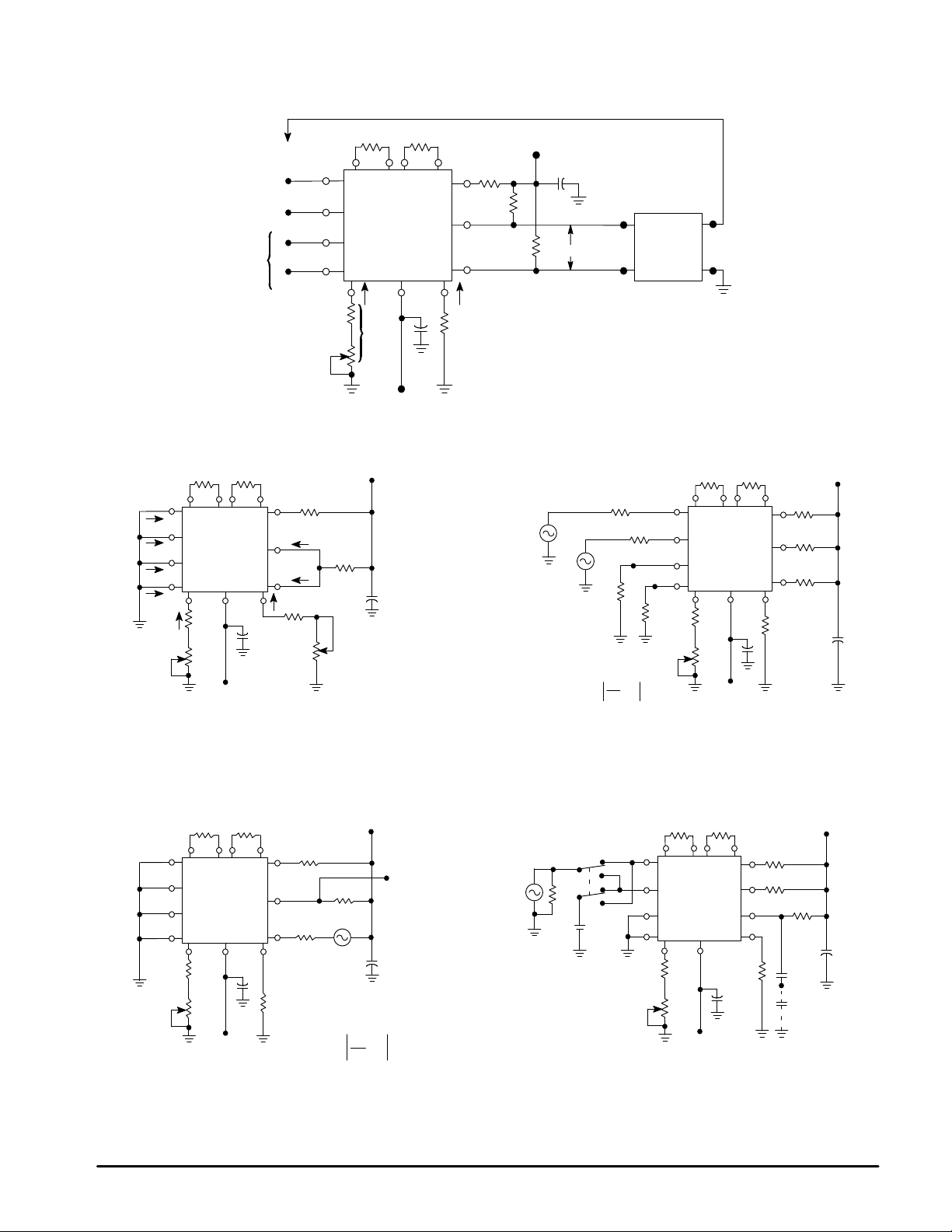
Figure 4. Linearity (Using Null T echnique)
µ
F
0.1
56 10 11
13 k
+
–
7
12 k
0.1 µF
MC1495
12 3 13
3.0 k
1
3.0 k
2
14
10 k
NOTE: Adjust “Scale Factor Adjust” for a null in VE.This schematic for
3.0 k
2
3
33 k
Output
Offset
Adjust
illustrative purposes only, not specified for test conditions.
40 k
7
MC1741C
1
4
500 500
10 k
8
10 k
6
5
Q4
4.0 k
2
3
+
–
10 k
7
MC1741C
1
4
9
12
11
10
13
8
5
X Input
6
V+
+15 V
V–
–15 V
V
E
MOTOROLA ANALOG IC DEVICE DATA
3
Page 4
MC1495
Figure 5. Linearity (Using X-Y Plotter Technique)
V
Offset Adjust
(See Figures 13 and 14)
To Pin
4 or 9
Y
V
Z
Y
X
Scale
Factor
RY = 15 k RX = 15 k
56 1011
4
9
8
MC1495
12
3
I
713
3
12 k
5.0 k
R3
0.1 µF
1
RL1 = 11 k
2
14
I
13
R13 = 13.7 k
R1
9.1 k
RL1 = 11 k
32 V
0.1 µF
+
–
Plotter
V
Y-Input
O
X–Y
Plotter
Plotter
X-Input
Adjust
–15 V
Figure 6. Input and Output Current Figure 7. Input Resistance
5.6 k
+ 32 V
0.1
e
2
1.0 M
4
9
8
12
RY = 15 k RX = 15 k
56 10 11
MC1495
3713
12 k
5.0 k
0.1
µ
F
–15 V
e1 = 1.0 Vrms
20 Hz
e
1
µ
F
R
= R
inX
inY
e
1
= R
1.0 M
1.0 M
1.0 M
e
2
e
1
–2
e
2
RY = 15 k RX = 15 k
56 10 11
4
9
I
4
MC1495
8
I
9
12
I
8
3713
I
12
12 k
I3 = 1.0 mA
Scale
Factor
Adjust
5.0 k
–15 V
14
0.1 µF
9.1 k
1
I
2
2
I
14
I13 = 1.0 mA
12 k
5.0 k
1
2
11 k
14
13.75 k
9.1 k
11 k
0.1
+ 32 V
µ
F
+
–
Figure 8. Output Resistance Figure 9. Bandwidth (RL = 11 kΩ)
RL = 11 k
e
1
1.0 Vrms
20 Hz
L
+ 32 V
e
1
e
2
56 10 11
Scale
Factor
Adjust
12
4
9
8
MC1495
3
12 k
5.0 k
–15 V
ein = 1.0 Vrms
e
2
µ
F
0.1
–2
e
in
50
+
1.0 V
–
MOTOROLA ANALOG IC DEVICE DATA
RY = 15 k RX = 15 k RY = 15 k RX = 15 k
56 10
4
9
8
12
3713
12 k
Scale
Factor
Adjust
5.0 k
MC1495
–15V
0.1
11
9.1 k
1
2
11 k
14
13.7 k
µ
F
RO = R
4
+ 32 V
9.1 k
1
11 k
2
14
13
7
R13
13.7 k
0.1
µ
F
11 k
e
o
CL < 3.0 pF
0.1
µ
F
Page 5
MC1495
ein = 1.0 Vrms
e
in
K = 40
6.2 V
Figure 10. Bandwidth (RL = 50 Ω)
RY = 510 RX = 510
56 10 11
4
9
50
+
1.0 V
–
Scale
Factor
Adjust
MC1495
8
12
37
12 k
5.0 k
–15V
13.7k
0.1
R13
µ
F
1
2
14
13
Figure 12. Power Supply Sensitivity
+ 32 V
2.0 k
4.3 k
15 k 15 k
56 10 11
4
9
MC1495
8
12
37 13
13.7 k
0.1
µ
F
1.0 k
50
e
1
2
14
VO2V
+ 15 V
50
o
CL < 3.0 pF
+ 32 V (V+)
9.1 k
11 k
11 k
O1
0.1
Figure 11. Common Mode Gain and
Common Mode Input Swing
15 k
CMV
X
(f = 20 Hz)
+
50
–
+
50
µ
F
CMV
Y
(f = 20 Hz)
–
12 k
5.0 k
15 k
56 10 11
4
9
8
MC1495
12
3
1.0 mA
µ
F
0.1
7
–15 V
13
12 k
5.0 k
1
2
14
1.0 mA
+ 32 V
9.1 k
11 k
+
11 k
V
O
ACM = 20 log
or 20 log
0.1
V
CMV
V
O
CMV
µ
F
O
Y
X
Figure 13. Offset Adjust Circuit
+
V
R
2.0 k
0.1
Pot #1
To Pin 8
Y Offset
Adjust
µ
F
V+15 V 32 V
R 10 k 22 k
10 k 10 k
10 k
Pot #2
T o Pin 12
X Offset
Adjust
2.0 k
2N2905A
or Equivalent
–15 V
22 k
–15 V
(V–)
|∆ (VO1 – VO2)|
S+ =
S– =
∆
V+
|
∆
(VO1 – VO2)|
∆
V–
Figure 14. Offset Adjust Circuit (Alternate)
+
V
R
Pot #1 Pot #2
To Pin 8
Y Offset
Adjust
V+15 V 32 V
R 2.0 k 5.1 k
10 k 10 k
2.0 k
–15 V
T o Pin 12
X Offset
Adjust
5.1 V
–15 V
5.1 V
MOTOROLA ANALOG IC DEVICE DATA
5
Page 6

Figure 15. Linearity versus T emperature Figure 16. Scale Factor versus T emperature
2.0
1.8
1.6
1.4
1.2
1.0
0.8
0.6
RX RY
E , E LINEARITY (%)
0.4
0.2
0
–55 –25 0 25 50 75 100 125
TA , AMBIENT TEMPERATURE (°C)
E
RY
E
RX
MC1495
K, SCALE FACTOR
0.110
0.105
K Adjusted to 0.100 at 25°C
0.100
0.095
–55 –25 0 25 50 75 100 125
TA , AMBIENT TEMPERATURE (
°
C)
Figure 17. Error Contributed by Input
Differential Amplifier
1.0
0.8
0.6
0.4
0.2
ERROR, PERCENT OF FULL SCALE (%)
0
10 12 14 16 18 20
VX = VY =± 10 V Max
I3 = I13 = 1.0 mAdc
RX or RY (k
Ω
)
Figure 19. Maximum Allowable Input V oltage versus Voltage at Pin 1 or Pin 7
14
12
pk
10
ERROR, PERCENT OF FULL SCALE (%)
1.0
0.8
0.6
0.4
0.2
Figure 18. Error Contributed by
Input Differential Amplifier
VX = VY = ± 5.0 V Max
I3 = I13 = 1.0 mAdc
0
4.0
6.0 8.0 10 12 14
Ω
RX or RY (k
)
8.0
6.0
4.0
XY
|V | or | V |, MAXIMUM (V )
2.0
0
0 2.0 4.0 6.0 8.0 10 12 14 16 18
6
Minimum
Recommended
|V1| or |V7| (V)
MOTOROLA ANALOG IC DEVICE DATA
Page 7

MC1495
OPERATION AND APPLICATIONS INFORMATION
Theory of Operation
The MC1495 is a monolithic, four-quadrant multiplier
which operates on the principle of variable
transconductance. A detailed theory of operation is covered
in Application Note AN489,
the MC1595
. The result of this analysis is that the differential
Analysis and Basic Operation of
output current of the multiplier is given by:
2VXV
IA – IB = ∆I =
RXRYI
Y
3
where, IA and IB are the currents into Pins 14 and 2,
respectively, and VX and VY are the X and Y input voltages at
the multiplier input terminals.
DESIGN CONSIDERATIONS
General
The MC1495 permits the designer to tailor the multiplier to
a specific application by proper selection of external
components. External components may be selected to
optimize a given parameter (e.g. bandwidth) which may in
turn restrict another parameter (e.g. maximum output voltage
swing). Each important parameter is discussed in detail in the
following paragraphs.
Linearity, Output Error, ERX or E
Linearity error is defined as the maximum deviation of
output voltage from a straight line transfer function. It is
expressed as error in percent of full scale (see figure below).
V
O
+10 V
For example, if the maximum deviation, V
±100 mV and the full scale output is 10 V, then the
percentage error is:
ER =
VE(max)
VO(max
x 100 =
)
100 x 10
Linearity error may be measured by either of the following
methods:
1.Using an X-Y plotter with the circuit shown in Figure 5,
obtain plots for X and Y similar to the one shown above.
2.Use the circuit of Figure 4. This method nulls the level
shifted output of the multiplier with the original input.The
peak output of the null operational amplifier will be equal
to the error voltage, VE
One source of linearity error can arise from large signal
nonlinearity in the X and Y input differential amplifiers. To
avoid introducing error from this source, the emitter
degeneration resistors RX and RY must be chosen large
enough so that nonlinear base-emitter voltage variation can
be ignored. Figures 17 and 18 show the error expected from
this source as a function of the values of RX and RY with an
operating current of 1.0 mA in each side of the differential
amplifiers (i.e., I3 = I13 = 1.0 mA).
+10V
Vx or V
10
(max)
RY
V
E(max)
y
–3
x 100 = ±1.0%.
.
E(max)
, is
3 dB Bandwidth and Phase Shift
Bandwidth is primarily determined by the load resistors
and the stray multiplier output capacitance and/or the
operational amplifier used to level shift the output. If
wideband operation is desired, low value load resistors
and/or a wideband operational amplifier should be used.
Stray output capacitance will depend to a large extent on
circuit layout.
Phase shift in the multiplier circuit results from two
sources: phase shift common to both X and Y channels (due
to the load resistor-output capacitance pole mentioned
above) and relative phase shift between X and Y channels
(due to differences in transadmittance in the X and Y
channels). If the input to output phase shift is only 0.6°, the
output product of two sine waves will exhibit a vector error of
1%. A 3° relative phase shift between VX and VY results in a
vector error of 5%.
Maximum Input V oltage
V
X(max)
, V
input voltages must be such that:
Y(max)
V
VY(max) <I3 R
X(max)
<I13 R
Y
Y
Exceeding this value will drive one side of the input amplifier
to “cutoff” and cause nonlinear operation.
Current I3 and I13 are chosen at a convenient value
(observing power dissipation limitation) between 0.5 mA and
2.0 mA, approximately 1.0 mA. Then RX and RY can be
determined by considering the input signal handling
requirements.
For V
The equation IA – IB =
is derived from IA – IB =
with the assumption RX >>
X(max)
RX = RY >
= V
Y(max)
10 V
1.0 mA
2VX V
RX RY I
(RX +
2kT
qI
13
= 10 V;
= 10 kΩ.
Y
3
2VX V
2kT
(RY +
)
qI
13
and RY >>
Y
2kT
)
I
3
qI
3
2kT
.
qI
3
At TA = +25°C and I13 = I3 = 1.0 mA,
2kT
2kT
= = 52 Ω.
qI
qI
13
3
Therefore, with RX = RY = 10 kΩ the above assumption is
valid. Reference to Figure 19 will indicate limitations of
V
X(max)
or V
due to V1 and V7. Exceeding these limits
Y(max)
will cause saturation or “cutoff” of the input transistors. See
Step 4 of General Design Procedure for further details.
Maximum Output V oltage Swing
The maximum output voltage swing is dependent upon the
factors mentioned below and upon the particular circuit being
considered.
For Figure 20 the maximum output swing is dependent
upon V+ for positive swing and upon the voltage at Pin 1 for
negative swing. The potential at Pin 1 determines the
quiescent level for transistors Q5, Q6, Q7 and Q8. This
potential should be related so that negative swing at Pins 2 or
14 does not saturate those transistors. See General Design
Procedure for further information regarding selection of
these potentials.
MOTOROLA ANALOG IC DEVICE DATA
7
Page 8
MC1495
Figure 20. Basic Multiplier
+
V
R
9
V
X
V
Y
12
4
8
R3
+
–
+
–
3
If an operational amplifier is used for level shift, as shown
in Figure 21, the output swing (of the multiplier) is greatly
reduced. See Section 3 for further details.
X
11
I
3
R
Y
5610
MC1495
13 7
R13
R
1
+
–
–
V
R
I
14
L
R
2
L
V
VO = K VX V
2R
L
K =
RX RY I
O
Y
3
Figure 21. Multiplier with Operational Amplifier Level Shift
– 15 V
GENERAL DESIGN PROCEDURE
Selection of component values is best demonstrated by
the following example. Assume resistive dividers are used at
the X and Y-inputs to limit the maximum multiplier input to ±
5.0 V [VX = V
(see Figure 21). If an overall scale factor of 1/10 is desired,
VX′ V
VO =
then,
Therefore, K = 4/10 for the multiplier (excluding the divider
network).
Step 1
. The fist step is to select current I3 and current I13.
There are no restrictions on the selection of either of these
currents except the power dissipation of the device. I3 and I
will normally be 1.0 mA or 2.0 mA. Further, I3 does not have
to be equal to I13, and there is normally no need to make
them different. For this example, let
] for a ± 10 V input [VX′ = V
Y(max)
(2VX) (2VY)
Y′
=
10
10
I3 = I13 = 1.0 mA.
– 15 V
= 4/10 VX V
Y′(max)
Y
13
]
–10V
–10V
V
′
Y
V
X
′
≤
VX ≤ +10V
≤
VY ≤ +10V
10 k
10 k
10 k
10 k
10
4
V
Y
9
V
X
R3
Scale
Factor
Adjust
+15 V
R
R
X
10 k
10 k
11
+
+
3
12 k
P
5
MC1495
13 8 12
I
13
R13
12 k
5.0 k
3
Y Offset
Adjust
2.0 k
5.1 V
+15 V
0.1 µF
6
VO =
–VX V
10
Y
20 k
R
L
0.1 µF
4
5
Y
6
I
3
10 k
R1
3.0 k
17
2
+
14
–
R
L
X Offset
P
1
Adjust
P
2
2.0 k
10 k
5.1 V
R0
3.0 k
18 k
5.0 k
P
4
R0
3.0 k
Output
Offset
Adjust
–15 V
3
2
7
+
MC1741C
–
1
8
MOTOROLA ANALOG IC DEVICE DATA
Page 9

MC1495
To set currents I3 and I13 to the desired value, it is only
necessary to connect a resistor between Pin 13 and ground,
and between Pin 3 and ground. From the schematic shown in
Figure 3, it can be seen that the resistor values necessary are
given by:
R13 + 500 Ω =
R3 + 500 Ω =
Let V– = –15 V, then R13 + 500 =
Let R13 = 12 kΩ. Similarly, R3 = 13.8 kΩ, let R3 = 15 kΩ
However, for applications which require an accurate scale
factor, the adjustment of R3 and consequently, I3, offers a
convenient method of making a final trim of the scale factor.
For this reason, as shown in Figure 21, resistor R3 is shown
as a fixed resistor in series with a potentiometer.
For applications not requiring an exact scale factor
(balanced modulator, frequency doubler, AGC amplifier, etc.)
Pins 3 and 13 can be connected together and a single
resistor from Pin 3 to ground can be used. In this case, the
single resistor would have a value of 1/2 the above calculated
value for R13.
Step 2
. The next step is to select RX and RY. T o insure that
the input transistors will always be active, the following
conditions should be met:
V
X
< I13,
R
X
A good rule of thumb is to make I3RY ≥ 1.5 V
I13 RX ≥ 1.5 V
. The larger the I3RY and I13RX product in
X(max)
relation to VY and VX respectively, the more accurate the
multiplier will be (see Figures 17 and 18).
Let RX = RY= 10 kΩ,
then I3RY = 10 V
I13R
X
since V
X(max)
= V
Y(max)
is sufficient.
Step 3
. Now that RX, RY and I3 have been chosen, RL can
be determined:
K =
2R
RX RY I
L
4
=
10
3
Thus RL = 20 kΩ.
Step 4
. To determine what power supply voltage is
necessary for this application, attention must be given to the
circuit schematic shown in Figure 3. From the circuit
schematic it can be seen that in order to maintain transistors
Q1, Q2, Q3 and Q4 in an active region when the maximum
input voltages are applied (VX′ = VY′ = 10 V or VX = 5.0 V,
VY = 5.0 V), their respective collector voltage should be at
least a few tenths of a volt higher than the maximum input
|V–| –0.7 V
I
13
|V–| –0.7 V
I
3
14.3 V
or R13 = 13.8 kΩ
1.0 mA
V
Y
< I
3
R
Y
and
Y(max)
= 10 V
= 5.0 V, the value of RX= RY = 10 kΩ
, or
(2) (RL)
(10 k) (10 k) (1.0 mA)
4
=
10
voltage. It should also be noticed that the collector voltage of
transistors Q3 and Q4 is at a potential which is two
diode-drops below the voltage at Pin 1. Thus, the voltage at
Pin 1 should be about 2.0 V higher than the maximum input
voltage. Therefore, to handle +5.0 V at the inputs, the voltage
at Pin 1 must be at least +7.0 V. Let V1 = 9.0 Vdc.
Since the current flowing into Pin 1 is always equal to 2I3,
the voltage at Pin 1 can be set by placing a resistor (R1) from
Pin 1 to the positive supply:
V+ –V
R1 =
Let V+ = 15 V, then R1 =
2I
3
1
15 V –9.0 V
(2) (1.0 mA)
R1 = 3.0 kΩ.
Note that the voltage at the base of transistors Q5, Q6, Q
and Q8 is one diode-drop below the voltage at Pin 1. Thus, in
order that these transistors stay active, the voltage at Pins 2
and 14 should be approximately halfway between the voltage
at Pin 1 and the positive supply voltage. For this example, the
voltage at Pins 2 and 14 should be approximately 1 1 V.
Step 5
. For dc applications, such as the multiply, divide
and square-root functions, it is usually desirable to convert
the differential output to a single-ended output voltage
referenced to ground. The circuit shown in Figure 22
performs this function. It can be shown that the output voltage
of this circuit is given by:
VO = (I2 –I14) R
And since IA –IB = I2 –I14 =
then VO =
2RL VX′ VY′
4RX RX I
3
where, VX′ VY′ is the voltage at
2IX I
I
3
L
2VXV
Y
=
I3RXR
Y
Y
the input to the voltage dividers.
Figure 22. Level Shift Circuit
+
V
R
V
I
I
14
2
2
V
14
R
R
O
L
O
+
V
–
R
L
O
The choice of an operational amplifier for this application
should have low bias currents, low offset current, and a high
common mode input voltage range as well as a high common
mode rejection ratio. The MC1456, and MC1741C
operational amplifiers meet these requirements.
7
MOTOROLA ANALOG IC DEVICE DATA
9
Page 10

MC1495
Referring to Figure 21, the level shift components will be
determined. When VX = VY = 0, the currents I2 and I14 will be
equal to I13. In Step 3, RL was found to be 20 kΩ and in Step
4, V2 and V14 were found to be approximately 1 1 V . From this
information RO can be found easily from the following
equation (neglecting the operational amplifiers bias current):
V2
+ I13
R
L
And for this example,
V+ –V
=
11 V
20 kΩ
2
R
O
+ 1.0 mA =
15 V –1 1 V
R
O
Solving for RO: RO = 2.6 kΩ, thus, select RO = 3.0 kΩ
For RO = 3.0 kΩ, the voltage at Pins 2 and 14 is calculated
to be:
V2 = V14 = 10.4 V.
The linearity of this circuit (Figure 21) is likely to be as
good or better than the circuit of Figure 5. Further
improvements are possible as shown in Figure 23 where R
has been increased substantially to improve the Y linearity,
and RX decreased somewhat so as not to materially affect
the X linearity . This avoids increasing RL significantly in order
to maintain a K of 0.1.
Figure 23. Multiplier with Improved Linearity
The versatility of the MC1495 allows the user to to
optimize its performance for various input and output signal
levels.
OFFSET AND SCALE FACTOR ADJUSTMENT
Offset Voltages
Within the monolithic multiplier (Figure 3) transistor baseemitter junctions are typically matched within 1.0 mV and
resistors are typically matched within 2%. Even with this
careful matching, an output error can occur. This output error
is comprised of X-input offset voltage, Y-input offset voltage,
and output offset voltage. These errors can be adjusted to
zero with the techniques shown in Figure 21. Offset terms
can be shown analytically by the transfer function:
VO = K[Vx ± V
Where: K = scale factor
Y
iox
± V
x(off)
] [Vy ± V
ioy
Vx= ‘‘x’’ input voltage
Vy= ‘‘y’’ input voltage
V
= ‘‘x’’ input offset voltage
iox
V
= ‘‘y’’ input offset voltage
ioy
V
V
= ‘‘x’’ input offset adjust voltage
x(off)
= ‘‘y’’ input offset adjust voltage
y(off)
VOO= output offset voltage.
± V
y(off)
] ± V
OO
(1)
±
V
Y
10 V
V
X
7
MC1741C
1
– 15 V
4
40 k
+15 V
6
5
VO =
–VX V
10
Y
– 15 V
3.0 k3.0 k
Output
Offset
Adjust
–15 V
3
+
2
–
20 k
3.0 k
17
14
–
++
X Offset
Adjust
2
33 k
10 k
15 k
2.0 k
7.5 k
10
10 k
10 k
4
9
13 k
5.0 k
Scale
Factor
Adjust
+15 V
+
3
10 k
′
10 k
′
27 k
5
11
13 8 12
15 k
6
MC1495
12 k
Y Offset
Adjust
20 k
2.0 k
10
MOTOROLA ANALOG IC DEVICE DATA
Page 11

MC1495
X, Y and Output Offset Voltages
V
O
X Offset Y Offset
Output
Offset
V
x
For most dc applications, all three offset adjust
potentiometers (P1, P2, P4) will be necessary. One or more
offset adjust potentiometers can be eliminated for ac
applications (see Figures 28, 29, 30, 31).
If well regulated supply voltages are available, the offset
adjust circuit of Figure 13 is recommended. Otherwise, the
circuit of Figure 14 will greatly reduce the sensitivity to power
supply changes.
Scale Factor
The scale factor K is set by P3 (Figure 21). P3 varies I
which inversely controls the scale factor K. It should be noted
that current I3 is one-half the current through R1. R1 sets the
bias level for Q5, Q6, Q7, and Q8 (see Figure 3). Therefore, to
be sure that these devices remain active under all conditions
of input and output swing, care should be exercised in
adjusting P3 over wide voltage ranges (see General Design
Procedure).
Adjustment Procedures
The following adjustment procedure should be used to null
the offsets and set the scale factor for the multiply mode of
operation, (see Figure 21).
1. X-Input Offset
(a) Connect oscillator (1.0 kHz, 5.0 Vpp sinewave)
to the Y-input (Pin 4).
(b) Connect X-input (Pin 9) to ground.
(c) Adjust X offset potentiometer (P2) for an ac
null at the output.
2. Y-Input Offset
(a) Connect oscillator (1.0 kHz, 5.0 Vpp sinewave)
to the X-input (Pin 9).
(b) Connect Y-input (Pin 4) to ground.
(c) Adjust Y offset potentiometer (P1) for an ac null
at the output.
3. Output Offset
(a) Connect both X and Y-inputs to ground.
(b) Adjust output offset potentiometer (P4) until
the output voltage (VO) is 0 Vdc.
4. Scale Factor
(a) Apply +10 Vdc to both the X and Y-inputs.
(b) Adjust P3 to achieve + 10 V at the output.
5. Repeat steps 1 through 4 as necessary.
The ability to accurately adjust the MC1495 depends upon
the characteristics of potentiometers P1 through P4.
Multi-turn, infinite resolution potentiometers with low
temperature coefficients are recommended.
Output
V
O
Offset
V
y
DC APPLICA TIONS
Multiply
The circuit shown in Figure 21 may be used to multiply
signals from dc to 100 kHz. Input levels to the actual
multiplier are 5.0 V (max). With resistive voltage dividers the
maximum could be very large however, for this application
two-to-one dividers have been used so that the maximum
input level is 10 V. The maximum output level has also been
designed for 10 V (max).
Squaring Circuit
If the two inputs are tied together, the resultant function is
squaring; that is VO = KV2 where K is the scale factor. Note
that all error terms can be eliminated with only three
adjustment potentiometers, thus eliminating one of the input
offset adjustments. Procedures for nulling with adjustments
are given as follows:
A. AC Procedure:
3
1. Connect oscillator (1.0 kHz, 15 Vpp) to input.
2. Monitor output at 2.0 kHz with tuned voltmeter
and adjust P3 for desired gain. (Be sure to peak
response of the voltmeter.)
3. Tune voltmeter to 1.0 kHz and adjust P1 for a
minimum output voltage.
4. Ground input and adjust P4 (output offset) for
0 Vdc output.
5. Repeat steps 1 through 4 as necessary.
B. DC Procedure:
1. Set VX = VY = 0 V and adjust P4 (output offset
potentiometer) such that VO = 0 Vdc
2. Set VX = VY = 1.0 V and adjust P1 (Y-input offset
potentiometer) such that the output voltage is
+ 0.100 V.
3. Set VX = VY = 10 Vdc and adjust P3 such that
the output voltage is + 10 V.
4. Set VX = VY = –10 Vdc. Repeat steps 1 through
3 as necessary.
Figure 24. Basic Divide Circuit
KVX V
Y
X
I
R1
1
I
2
V
Z
R2
–
+
V
X
V
Y
MOTOROLA ANALOG IC DEVICE DATA
11
Page 12

MC1495
Divide Circuit
Consider the circuit shown in Figure 24 in which the
multiplier is placed in the feedback path of an operational
amplifier. For this configuration, the operational amplifier will
maintain a “virtual ground” at the inverting (–) input.
Assuming that the bias current of the operational amplifier is
negligible, then I1 = I2 and,
KVXV
R1
Solving for VY,VY =
If R1=R2, VY =
If R1= KR2, VY =
Hence, the output voltage is the ratio of VZ to VX and
provides a divide function. This analysis is, of course, the
ideal condition. If the multiplier error is taken into account, the
output voltage is found to be:
VY = –
where ∆E is the error voltage at the output of the multiplier.
From this equation, it is seen that divide accuracy is strongly
dependent upon the accuracy at which the multiplier can be
set, particularly at small values of VY. For example, assume
that R1 = R2, and K = 1/10. For these conditions the output of
the divide circuit is given by:
VY =
From Equation 6, it is seen that only when VX = 10 V is the
error voltage of the divide circuit as low as the error of the
multiply circuit. For example, when VX is small, (0.1 V) the
error voltage of the divide circuit can be expected to be a
hundred times the error of the basic multiplier circuit.
Y
=
R1
R2 K
–10 V
V
–V
–R1
R2 K
–V
KV
–V
Z
X
R2
V
Z
V
Z
V
X
Z
(1)
(2)
(3)
X
Z
(4)
X
V
+
E
∆
Z
+
V
KV
X
X
∆E
10
V
X
(5)
(6)
In terms of percentage error,
error
percentage error =
actual
x 100%
or from Equation (5),
∆E
PED =
KV
R1
R2 K
X
V
V
R2
=
R1∆EV
Z
Z
(7)
X
From Equation 7, the percentage error is inversely related
to voltage VZ (i.e., for increasing values of VZ, the percentage
error decreases).
A circuit that performs the divide function is shown in
Figure 25.
Two things should be emphasized concerning Figure 25.
1. The input voltage (VX′) must be greater than zero and
must be positive. This insures that the current out of
Pin 2 of the multiplier will always be in a direction
compatible with the polarity of VZ.
2. Pin 2 and 14 of the multiplier have been interchanged in
respect to the operational amplifiers input terminals. In
this instance, Figure 25 differs from the circuit
connection shown in Figure 21; necessitated to insure
negative feedback around the loop.
A suggested adjustment procedure for the divide circuit.
1. Set VZ = 0 V and adjust the output offset potentiometer
(P4) until the output voltage (VO) remains at some (not
necessarily zero) constant value as VX′ is varied
between +1.0 V and +10 V.
2. Keep VZ at 0 V , set VX′ at +10 V and adjust the Y input
offset potentiometer (P1) until VO = 0 V.
3. Let VX′ = VZ and adjust the X-input offset potentiometer
(P2) until the output voltage remains at some (not
necessarily – 10 V) constant value as VZ = VX′ is varied
between +1.0 and +10 V.
4. Keep VX′ = VZ and adjust the scale factor potentiometer
(P3) until the average value of VO is –10 V as VZ = VX′ is
varied between +1.0 V and +10 V.
5. Repeat steps 1 through 4 as necessary to achieve
optimum performance.
12
– 15 V – 15 V
µ
F
20 k
≤
V
0
X
≤
0.1
4
6
5
≤ +10 V
′
VZ ≤ +10 V
0.1 µF
R
4
9
5.0 k
10
3
R
10 k
+
13 k
P
3
10 k
10 k
10 k
V
X
′
10 k
Scale
Factor
Adjust
Y
X
10 k
11
5
6
MC1495
13 8 12
12 k
To Offset
Adjust
(See Figure 13)
3.0 k3.0 k3.9 k
17
14
–
2
++
18 k
5.0 k
Output
P
4
Offset
Adjust
3
2
7
+
MC1741C
–
1
–10 V
+15 V
V
O
VO =
V
Z
–10 V
V
X
Z
MOTOROLA ANALOG IC DEVICE DATA
Figure 25. Divide Circuit
Page 13

MC1495
Figure 26. Basic Square Root Circuit
2
KV
O
MC1495
–
V
Z
+
–
+
Square Root
A special case of the divide circuit in which the two inputs
to the multiplier are connected together is the square root
function as indicated in Figure 26. This circuit may suffer from
latch-up problems similar to those of the divide circuit. Note
that only one polarity of input is allowed and diode clamping
(see Figure 27) protects against accidental latch-up.
This circuit also may be adjusted in the closed-loop mode
as follows:
1. Set VZ to –0.01 V and adjust P4 (output offset) for
VO = +0.316 V, being careful to approach the output
from the positive side to preclude the effect of the output
diode clamping.
2. Set VZ to –0.9 V and adjust P2 (X adjust) for
VO = +3.0 V.
3. Set VZ to –10 V and adjust P3 (scale factor adjust)
for VO = +10 V.
4. Steps 1 through 3 may be repeated as necessary to
achieve desired accuracy.
+
+
V
= –V
or
O
Z
|VZ|
K
KV
O
VO =
2
AC APPLICATIONS
The applications that follow demonstrate the versatility of
the monolithic multiplier. If a potted multiplier is used for these
cases, the results generally would not be as good because
the potted units have circuits that, although they optimize dc
multiplication operation, can hinder ac applications.
Frequency doubling often is done with a diode where
the fundamental plus a series of harmonics are
generated. However, extensive filtering is required to obtain
the desired harmonic, and the second harmonic obtained
under this technique usually is small in magnitude and
requires amplification.
When a multiplier is used to double frequency the second
harmonic is obtained directly , except for a dc term, which can
be removed with ac coupling.
eo = KE2 cos2 ωt
eo =
(1 + cos 2ωt).
2
2
KE
A potted multiplier can be used to obtain the double
frequency component, but frequency would be limited by its
internal level-shift amplififer. In the monolithic units, the
amplifier is omitted.
In a typical doubler circuit, conventional ± 15 V supplies
are used. An input dynamic range of 5.0 V peak-to-peak is
allowed. The circuit generates wave-forms that are double
frequency; less than 1% distortion is encountered without
filtering. The configuration has been successfully used in
excess of 200 kHz; reducing the scale factor by decreasing
the load resistors can further expand the bandwidth.
Figure 29 represents an application for the monolithic
multiplier as a balanced modulator. Here, the audio input
signal is 1.6 kHz and the carrier is 40 kHz.
10 k
10 k
4
9
5.0 k
Scale
Factor
Adjust
R
X
10 k
11
10
+
3
13 8 12
13 k
P
3
Figure 27. Square Root Circuit
– 15 V – 15V
R
Y
10 k
5
6
MC1495
12 k
To Offset
Adjust
(See Figure 13)
17
2
–
14
++
5.0 k
13 k
P
4
3.0 k3.0 k3.9 k
3
2
Output
Offset
Adjust
7
+
MC1741C
–
1
–10
0.1
4
5
20 k
R
L
≤
VZ ≤ +0 V
µ
F
6
(11 V)
0.1 µF
+15 V
V
O
V
Z
VO =
√
10 |VZ|
MOTOROLA ANALOG IC DEVICE DATA
13
Page 14

MC1495
Figure 28. Frequency Doubler
R
R
8.2 k
5610
4
ω
t
E cos
(< 5.0 Vpp)
Offset
Adjust
When two equal cosine waves are applied to X and Y, the result
is a wave shape of twice the input frequency. For this example
the input was a 10 kHz signal, output was 20 kHz.
9
8
Y
12
3713
6.8 k
Y
8.2 k
MC1495
1.0 µF
X
–15 V
11
*Select
14
1
2
3.0 k
3.3 k
eo≈
Figure 29. Balanced Modulator
(A)
R
eY = E cos
eX = E cos
Offset
Adjust
ωmt
ω
R
8.2 k
5610
4
9
t
c
8
Y
12
X
3
6.8 k
Y
MC1495
–
1.0
µ
F
+
X
8.2 k
–15 V
11
713
*Select
14
1
2
3.0 k
3.3 k
(B)
VCC +15 V
R1
R1
R1
3.3 k
C1*
2
E
cos 2
20
+15 V
R
L
R
3.3 k
C1*
e
o
L
+
1.0
–
ω
+
1.0 µF
–
The defining equation for balanced modulation is
K(Emcos ωmt) (Ec cos ωct) =
KEc E
m
[ cos (ωc + ωm)t + cos (ωc – ωm) t ]
µ
F
2
where ωc is the carrier frequency, ωm is the modulator
frequency and K is the multiplier gain constant.
AC coupling at the output eliminates the need for level
translation or an operational amplifier; a higher operating
frequency results.
A problem common to communications is to extract the
intelligence from single-sideband received signal. The ssb
t
signal is of the form:
e
= A cos (ωc + ωm) t
ssb
and if multiplied by the appropriate carrier waveform, cos ωct,
e
ssbecarrier
AK
=
[cos (2ωc + ωm)t + cos (ωc) t ].
2
If the frequency of the band-limited carrier signal (ωc) is
ascertained in advance, the designer can insert a low pass
filter and obtain the (AK/2) (cosωct) term with ease. He/she
also can use an operational amplifier for a combination level
shift-active filter, as an external component. But in potted
multipliers, even if the frequency range can be covered, the
operational amplifier is inside and not accessible, so the user
must accept the level shifting provided, and still add a low
pass filter.
Amplitude Modulation
The multiplier performs amplitude modulation, similar to
balanced modulation, when a dc term is added to the
modulating signal with the Y-offset adjust potentiometer (see
Figure 30).
Here, the identity is:
Em(1 + m cos ωmt) Ec cos ωct = KEmEccos ωct
KEmEcm
[ cos(ωc + ωm)t + cos (ωc – ωm) t ]
2
+
where m indicates the degrees of modulation. Since m is
adjustable, via potentiometer P1, 100% modulation is
possible. Without extensive tweaking, 96% modulation may
be obtained where ωc and ωm are the same as in the
balanced modulator example.
Linear Gain Control
To obtain linear gain control, the designer can feed to one
of the two MC1495 inputs a signal that will vary the unit’s
gain. The following example demonstrates the feasibility of
this application. Suppose a 200 kHz sinewave, 1.0 V
peak-to-peak, is the signal to which a gain control will be
added. The dynamic range of the control voltage VC is 0 V to
+1.0 V. These must be ascertained and the proper values of
RX and RY can be selected for optimum performance. For the
200 kHz operating frequency, load resistors of 100 Ω were
chosen to broaden the operating bandwidth of the multiplier,
but gain was sacrificed. It may be made up with an amplifier
operating at the appropriate frequency (see Figure 31).
14
MOTOROLA ANALOG IC DEVICE DATA
Page 15

MC1495
Figure 30. Amplitude Modulation
11
14
*Select
VCC = +15 V
R1
1
3.0 k
R
L1
2
3.3 k
e
R
3.3 k
C1*
o
L1
eY = E cos
eX = E cos
% Modulation Adjust
ωmt
ωmt
Offset Adjust
eX, eY < 5.0 V
R
R
8.2 k
5610
4
9
8
Y
12
X
3713
pp
6.8 k
Y
MC1495
1.0 µF
X
8.2 k
–15 V
The signal is applied to the unit’s Y-input. Since the total
input range is limited to 1.0 Vpp, a 2.0 V swing, a current
source of 2.0 mA and an RY value of 1.0 kΩ is chosen. This
takes best advantage of the dynamic range and insures
linear operation in the Y-channel.
Since the X-input varies between 0 and +1.0 V , the current
source selected was 1.0 mA, and the RX value chosen
was 2.0 kΩ. This also insures linear operation over the
X-input dynamic range. Choosing RL = 100 assures wide
bandwidth operation.
Hence, the scale factor for this configuration is:
R
K =
=
=
L
RX RY I
3
100
(2 k) (1 k) (2 x 10³)
1
–1
V
40
–1
V
The 2 in the numerator of the equation is missing in this scale
factor expression because the output is single-ended and ac
coupled.
V
in
V
C
Offset
Adjust
1.0 k
0.1
51
µ
F
2.0 mA
Y
4
X
9
Y
8
X
12
5.0 k
2.0 k 1.0 k
1110
+
MC1495
+
k =
–
–
3
3.0 k
P
3
5
6
1
40
13 7
11 k
–12 V
Figure 31. Linear Gain Control
+12 V
1
1.5 k
2
100
100
14
+
1.0
µ
F
Amplifier
AV = 40
NOTE: Linear gain control of a 1.0 Vpp signal is performed with a 0 V
1.25
)
0.75
pp
(V
O
V
0.25
V
O
to 1.0 V control voltage. If VC is 0.5 V the output will be 0.5 Vpp.
Vin = 1.0 V
1.0
0.5
000.2 0.4 0.6 0.8 1.0 1.2
pp
200 kHz
V
AGC
(V)
MOTOROLA ANALOG IC DEVICE DATA
15
Page 16

–A–
14 8
–B–
P
7 PL
71
G
C
–T–
SEATING
PLANE
14 8
D 14 PL
0.25 (0.010) A
K
M
S
B
T
B
17
A
F
C
N
SEATING
HG D
PLANE
K
MC1495
OUTLINE DIMENSIONS
D SUFFIX
PLASTIC PACKAGE
CASE 751A–03
ISSUE F
M
0.25 (0.010) B
X 45
R
S
PLASTIC PACKAGE
L
J
M
M
_
M
P SUFFIX
CASE 646–06
ISSUE L
NOTES:
1. DIMENSIONING AND TOLERANCING PER ANSI
Y14.5M, 1982.
2. CONTROLLING DIMENSION: MILLIMETER.
3. DIMENSIONS A AND B DO NOT INCLUDE
MOLD PROTRUSION.
4. MAXIMUM MOLD PROTRUSION 0.15 (0.006)
PER SIDE.
5. DIMENSION D DOES NOT INCLUDE DAMBAR
PROTRUSION. ALLOWABLE DAMBAR
PROTRUSION SHALL BE 0.127 (0.005) TOTAL
IN EXCESS OF THE D DIMENSION AT
MAXIMUM MATERIAL CONDITION.
F
J
DIM MIN MAX MIN MAX
A 8.55 8.75 0.337 0.344
B 3.80 4.00 0.150 0.157
C 1.35 1.75 0.054 0.068
D 0.35 0.49 0.014 0.019
F 0.40 1.25 0.016 0.049
G 1.27 BSC 0.050 BSC
J 0.19 0.25 0.008 0.009
K 0.10 0.25 0.004 0.009
M 0 7 0 7
____
P 5.80 6.20 0.228 0.244
R 0.25 0.50 0.010 0.019
NOTES:
1. LEADS WITHIN 0.13 (0.005) RADIUS OF TRUE
POSITION AT SEATING PLANE AT MAXIMUM
MATERIAL CONDITION.
2. DIMENSION L TO CENTER OF LEADS WHEN
FORMED PARALLEL.
3. DIMENSION B DOES NOT INCLUDE MOLD
FLASH.
4. ROUNDED CORNERS OPTIONAL.
DIM MIN MAX MIN MAX
A 0.715 0.770 18.16 19.56
B 0.240 0.260 6.10 6.60
C 0.145 0.185 3.69 4.69
D 0.015 0.021 0.38 0.53
F 0.040 0.070 1.02 1.78
G 0.100 BSC 2.54 BSC
H 0.052 0.095 1.32 2.41
J 0.008 0.015 0.20 0.38
K 0.115 0.135 2.92 3.43
L 0.300 BSC 7.62 BSC
M 0 10 0 10
____
N 0.015 0.039 0.39 1.01
INCHESMILLIMETERS
MILLIMETERSINCHES
Motorola reserves the right to make changes without further notice to any products herein. Motorola makes no warranty , representation or guarantee regarding
the suitability of its products for any particular purpose, nor does Motorola assume any liability arising out of the application or use of any product or circuit, and
specifically disclaims any and all liability, including without limitation consequential or incidental damages. “T ypical” parameters which may be provided in Motorola
data sheets and/or specifications can and do vary in different applications and actual performance may vary over time. All operating parameters, including “Typicals”
must be validated for each customer application by customer’s technical experts. Motorola does not convey any license under its patent rights nor the rights of
others. Motorola products are not designed, intended, or authorized for use as components in systems intended for surgical implant into the body, or other
applications intended to support or sustain life, or for any other application in which the failure of the Motorola product could create a situation where personal injury
or death may occur. Should Buyer purchase or use Motorola products for any such unintended or unauthorized application, Buyer shall indemnify and hold Motorola
and its officers, employees, subsidiaries, affiliates, and distributors harmless against all claims, costs, damages, and expenses, and reasonable attorney fees
arising out of, directly or indirectly, any claim of personal injury or death associated with such unintended or unauthorized use, even if such claim alleges that
Motorola was negligent regarding the design or manufacture of the part. Motorola and are registered trademarks of Motorola, Inc. Motorola, Inc. is an Equal
Opportunity/Affirmative Action Employer.
How to reach us:
USA/EUROPE /Locations Not Listed: Motorola Literature Distribution; JAPAN: Nippon Motorola Ltd.; Tatsumi–SPD–JLDC, 6F Seibu–Butsuryu–Center,
P.O. Box 20912; Phoenix, Arizona 85036. 1–800–441–2447 or 602–303–5454 3–14–2 Tatsumi Koto–Ku, Tokyo 135, Japan. 03–81–3521–8315
MFAX: RMF AX0@email.sps.mot.com – TOUCHT ONE 602–244–6609 ASIA/PACIFIC: Motorola Semiconductors H.K. Ltd.; 8B Tai Ping Industrial Park,
INTERNET: http://Design–NET.com 51 Ting Kok Road, Tai Po, N.T., Hong Kong. 852–26629298
16
◊
MOTOROLA ANALOG IC DEVICE DATA
MC1495/D
*MC1495/D*
 Loading...