

Page 1

The MC1494 is designed for use where the output voltage is a linear
product of two input voltages. Typical applications include: multiply, divide,
square root, mean square, phase detector, frequency doubler, balanced
modulator/ demodulator, electronic gain control.
The MC1494 is a variable transconductance multiplier with internal
level–shift circuitry and voltage regulator. Scale factor , input offsets and output
offset are completely adjustable with the use of four external potentiometers.
Two complementary regulated voltages are provided to simplify offset
adjustment and improve power supply rejection.
• Operates with ±15 V Supplies
• Excellent Linearity: Maximum Error (X or Y) ±1.0 %
• Wide Input Voltage Range: ±10 V
• Adjustable Scale Factor, K (0.1 nominal)
• Single–Ended Output Referenced to Ground
• Simplified Offset Adjust Circuitry
• Frequency Response (3.0 dB Small–Signal): 1.0 MHz
• Power Supply Sensitivity: 30 mV/V typical
Order this document by MC1494/D
LINEAR FOUR–QUADRANT
MULTIPLIER INTEGRATED
CIRCUIT
SEMICONDUCTOR
TECHNICAL DATA
16
1
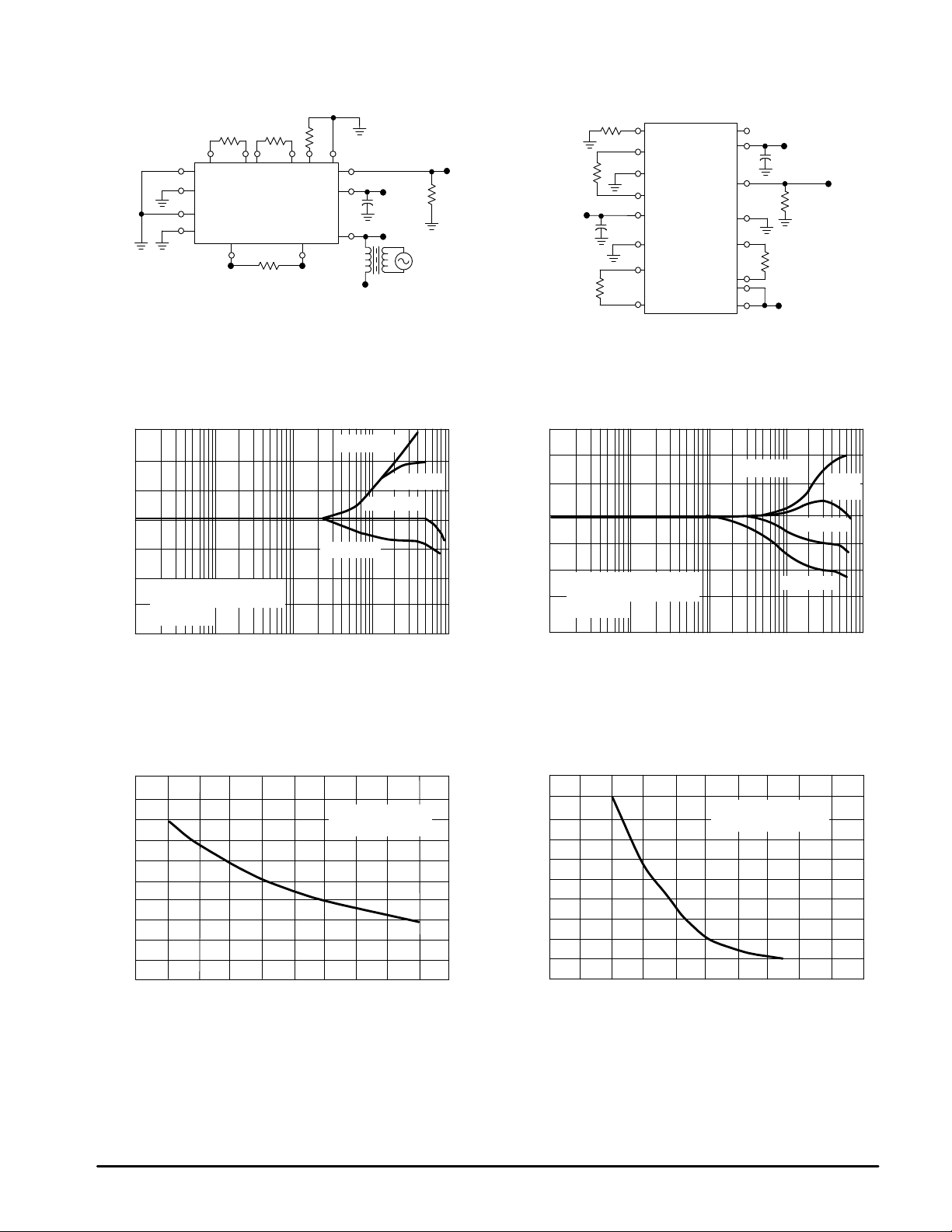
Figure 1. Multiplier Transfer Characteristic Figure 2. Linearity Error versus T emperature
10
8.0
6.0
4.0
2.0
0
– 2.0
– 4.0
, OUTPUT VOL TAGE (V)
O
V
– 6.0
– 8.0
–10
–10 – 8.0 – 6.0 – 4.0 – 2.0 0 2.0 4.0 6.0 8.0 10
X
Y
k =
VX, INPUT VOLTAGE (V)
+
KXY
1
10
P SUFFIX
PLASTIC PACKAGE
CASE 648C
ORDERING INFORMATION
Tested Operating
Device
MC1494P TA = 0° to + 70°C Plastic DIP
1.00
0.75
0.50
0.25
RX RY
E or E , LINEARITY ERROR (%)
0
– 50 0 50 125
– 25 25 75 100
Temperature Range
TA, AMBIENT TEMPERATURE (°C)
Package
MOTOROLA ANALOG IC DEVICE DATA
Motorola, Inc. 1996 Rev 0
1
Page 2

MC1494
MAXIMUM RATINGS
Power Supply Voltages ± V ± 18 Vdc
Differential Input Signal V9–V
Common Mode Input Voltage
V
= V9 = V
CMY
V
= V10 = V
CMX
Power Dissipation (Package Limitation)
TA = + 25°C
Derate above TA = + 25°C
Operating Temperature Range T
Storage Temperature Range T
(TA = + 25°C, unless otherwise noted.)
Rating Symbol Value Unit
±|6 + I1RY|<30
6
V10–V
V
6
13
CMY
V
CMX
1/θ
P
stg
13
D
JA
A
±|6 + I1RX|<30
±11.5
±11.5
1.25
20
0 to +70 °C
– 65 to +150 °C
mW/°C
Vdc
Vdc
W
ELECTRICAL CHARACTERISTICS (±V = ±15 V, T
unless otherwise noted.)
Characteristics
Linearity
Output error in percent of full scale
–10 V <VX < +10 V (VY = ±10 V)
–10 V <VY < +10 V (VX = ±10 V)
TA = +25°C
TA = T
Input
Voltage Range (VX = VY = Vin)
Resistance (X or Y Input)
Offset Voltage (X Input) (Note 1)
(Y Input) (Note 1)
Bias Current (X or Y Input)
Offset Current (X or Y Input)
Output
Voltage Swing Capability
Impedance
Offset Voltage (Note 1)
Offset Current (Note 1)
Temperature Stability (Drift)
TA = T
Output Offset (X = 0, Y = 0) Voltage
X Input Offset (Y = 0)
Y Input Offset (X = 0)
Scale Factor
Total DC Accuracy Drift (X = 10, Y = 10)
Dynamic Response
Small Signal (3.0 dB)
Power Bandwidth (47 k)
3° Relative Phase Shift
1% Absolute Error
Common Mode
Input Swing (X or Y)
Gain (X or Y)
Power Supply
Current
Quiescent Power Dissipation
Sensitivity
Regulated Offset Adjust Voltages
Positive/Negative
T emperature Coef ficient (VR+ or VR–)
Power Supply Sensitivity (VR+ or VR–)
NOTE: 1.Offsets can be adjusted to zero with external potentiomers. T
high
high
or T
to T
low
low
(Note 1)
= + 25°C, R1 = 16 kΩ, RX = 30 kΩ, RY = 62 kΩ, RL = 47 kΩ,
A
Current
Figure Symbol Min Typ Max Unit
= +70°C, T
High
3 ERX or E
4, 5, 6
5, 6
–
7
BW
BW
8
9
9
= 0°C
Low
V
in
R
in
|V
|
iox
|V
|
ioy
I
b
|Iio|
V
O
R
O
|VOO|
|IOO|
|TCVOO|
|TCIOO|
|TCV
iox
|TCV
ioy
|TCK|
|TCE|
3dB (X)
3dB (Y)
P
BW
fφ
fθ
CMV
A
CM
Id+
Id–
P
D
S+
S–
VR+, VR–
TCV
R
SR+, SR–
RY
|
|
–
–
±10
–
–
–
–
–
±10
–
–
–
–
–
–
–
–
–
–
–
–
–
–
±10.5
–
–
–
–
–
–
3.5
–
–
±0.5
–
–
300
0.2
0.8
1.0
50
–
850
1.2
25
1.3
27
0.3
1.5
0.07
0.09
0.8
1.0
440
240
30
–
–65
6.0
6.5
185
13
30
4.3
0.03
0.6
±1.0
±1.3
–
–
2.5
2.5
2.5
400
–
–
2.5
52
–
–
–
–
–
–
–
–
–
–
–
–
–
12
12
350
100
200
5.0
–
–
%
V
pk
MΩ
V
µA
nA
V
pk
kΩ
V
µA
mV/°C
nA/°C
mV/°C
%/°C
MHz
kHz
V
pk
dB
mAdc
mW
mV/V
Vdc
mV/°C
mV/V
2
MOTOROLA ANALOG IC DEVICE DATA
Page 3
MC1494
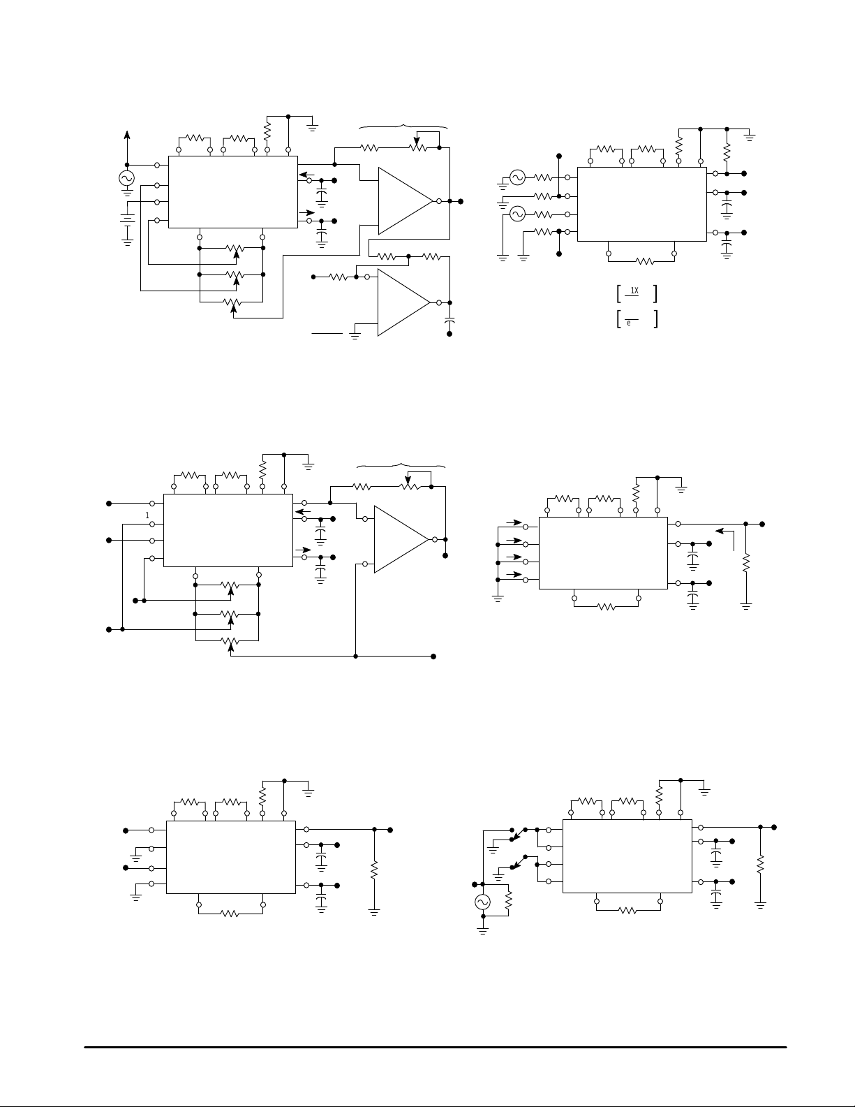
Figure 3. Linearity Figure 4. Input Resistance
E = 20 V
f = 20 Hz
10 V
V
X
V
Y
VX off
Adjust RL for a null in E
To A
pp
+
–
RX = 30 k RY = 62 k
11 12 7 8 1 3
VX 10
+
V
13
Y
–
+
9
–
6
MC1494
–+
V
R
4
20 k
20 k
50 k
R1 =
16 k
V
2
R
Linearity, Error =
14
15
A
5
E
E
I
15
0.1
I
5
0.1
10 k
o(peak)
S(peak)
+15 V
µ
F
–15 V
µ
F
22 k
–
MC1456
+
10 k 10 k
–
MC1456
+
Figure 5. Offset V oltages, Gain
o
R
L
50 k
0.1
f = 20 Hz e
e
V
O
e
1Y
µ
F
E
o
2X
1X
1.0 M
1.0 M
1.0 M
1.0 M
30 k 62 k
11 12 7 8 1 3
R
X
10
+
13
–
+
9
–
6
e
2Y
MC1494
–+
42
8.2 k
e
1X
Rin X =
Rin Y =
– 2
[]
e
2X
e
1Y
[
e
2Y
R
– 2
16 k
47 k
Y
Ω
M
M
Ω
]
V
O
14
15
+15 V
µ
F
0.1
5
–15 V
µ
F
0.1
Figure 6. Input Bias Current/Input Offset
Current, Output Resistance
R
–
MC1456
+
L
VO off
30 k 62 k
R
11 12
I
10
10
I
13
I
V
O
9
I
6
+
13
–
9
+
6
–
7813
X
MC1494
R
8.2 k
16 k
Y
14
+15 V
15
0.1 µF
5
+–
24
0.1
–15 V
µ
F
V
O
R
O
47 k
VY off
10
13
9
6
30 k 62 k
11 12
R
X
+
–
+
–
4
7813
R
Y
MC1494
–
+
20 k
20 k
50 k
16 k
2
14
15
5
I
15
I
5
+15 V
0.1
–15 V
0.1 µF
µ
F
22 k 50 k
Figure 7. Frequency Response Figure 8. Common Mode
30 k 62 k
R
11 12
10
V
X
V
Y
+
13
–
9
+
6
–
7813
X
MC1494
8.2 k
16 k
R
Y
14
15
+–
5
24
MOTOROLA ANALOG IC DEVICE DATA
0.1 µF
0.1
µ
CO = 3.0 pF
+15 V
–15 V
F
47 k
R
30 k 62 k
11 12
R
10
V
O
L
CMV
(20 Hz)
Y
51
+
13
–
9
+
6
–
7813
X
MC1494
8.2 k
16 k
R
Y
14
15
0.1 µF
5
+–
24
0.1
+15 V
–15 V
µ
F
V
47 k
O
3
Page 4
MC1494
Figure 9. Power Supply Sensitivity Figure 10. Burn–In
30 k 62 k
10
13
9
6
11 12
R
+
–
+
–
7813
X
MC1494
8.2 k
VR–V
16 k
R
Y
+–
24
+
R
Figure 11. Frequency Response of Y Input
versus Load Resistance
15
10
5.0
0
10
RL = 47 k
5
– 5.0
RELATIVE GAIN (dB)
–10
VY = 1.0 Vrms, VX = 10 Vdc
RX = 30 kΩ, RY = 62 k
–15
CO = 6.0 pF
–20
3
10
Ω
4
10
f, FREQUENCY (Hz)
14
15
0.1 µF
5
–15 V
RL = 1.0 k
RL = 33 k
Ω
6
10
+15 V
V
S
100 Hz
Ω
RL = 10 k
Ω
47 k
16 k 1
2
V
O
8.2 k
–15 V
0.1 µF
62 k
3
4
5
MC1494
6
7
8
16
NC
+15 V
15
0.1 µF
14
13
12
30 k
11
10
Vin – +10 V
9
47 k
V
O
Figure 12. Frequency Response of X Input
versus Load Resistance
15
10
Ω
5.0
0
– 5.0
RELATIVE GAIN (dB)
–10
VX = 1.0 Vrms, VY = 10 Vdc
RX = 30 kΩ, RY = 62 K
–15
Ω
CO = 6.0 pF
10
7
–20
10
3
10
4
f, FREQUENCY (Hz)
10
5
RL = 1.0 k
RL = 47 k
10
Ω
RL = 33 k
6
RL =
10 k
Ω
Ω
Ω
7
10
Figure 13. Linearity versus RX or RY with K = 1
RX RY
E or E , LINEARITY ERROR (%)
0.4
0.3
0.2
0.1
0
2.0 4.0 6.0 8.0
4.0 8.0 12 16 20
RL Adjusted for K = 1
Vin = 2.0 Vpp
4
10
RX (k
RY (k
Figure 14. Linearity versus RX or RY with K = 1/10
0.6
0.5
0.4
0.3
RX RY
E or E , LINEARITY ERROR (%)
0.2
Ω
)
Ω
)
20 30 40 50
40 60 80 100
RL Adjusted for K = 1/10
Vin = 20 Vpp
RX (kΩ)
RY (k
Ω
)
MOTOROLA ANALOG IC DEVICE DATA
Page 5
MC1494
Figure 15. Large Signal V oltage versus Frequency Figure 16. Scale Factor (K) versus T emperature
0.108
20
10
O
V , OUTPUT VOL TAGE (Vpp)
0
100 1.0 k 10 k 100 k
With MC1456 Buffer Op Amp
1
No Op Amp, RL = 47 k
2
f, FREQUENCY (Hz)
1
2
Ω
CIRCUIT DESCRIPTION
0.106
0.104
0.102
0.1
0.098
K, SCALE FACTOR
0.096
0.094
– 55 – 35 –15 5.0 25 45 65 85 105 125
TA, AMBIENT TEMPERATURE (
K Factor Adjusted for 1/10 at 25°C)
°
C)
145
Introduction
The MC1494 is a monolithic, four–quadrant multiplier that
operates on the principle of variable transconductance. It
features a single–ended current output referenced to ground
and provides two complementary regulated voltages for use
with the offset adjust circuits to virtually eliminate sensitivity
of the offset voltage nulls to changes in supply voltages.
As shown in Figure 17, the MC1494 consists of a multiplier
proper and associated peripheral circuitry to provide these
features.
Regulator
The regulator biases the entire MC1494 circuit making it
essentially independent of supply variation. It also provides
two convenient regulated supply voltages which can be used
in the offset adjust circuitry. The regulated output voltage at
Pin 2 is approximately + 4.3 V, while the regulated voltage at
Pin 4 is approximately – 4.3 V. For optimum temperature
stability of these regulated voltages, it is recommended that
|I2| = |I4| = 1.0 mA (equivalent load of 8.6 kΩ). As will be
shown later, there will normally be two 20 kΩ potentiometers
and one 50 kΩ potentiometer connected between Pins 2
and 4.
The regulator also establishes a constant current reference
that controls all of the constant current sources in the MC1494.
Note that all current sources are related to current I1 which is
determined by R1. For best temperatures performance, R1
should be 16 kΩ so that I1 ≈ 0.5 mA for all applications.
Multiplier
The multiplier section of the MC1494 (center section of
Figure 17) is nearly identical to the MC1495 and is discussed
in detail in Application Note AN489,
Operation of the MC1495
. The result of this analysis is that
Analysis and Basic
the differential output current of the multiplier is given by:
2VX V
IA – IB = ∆I
[
RXRYI
Y
1
Differential Current Converter
This portion of the circuitry converts the differential output
current (IA –IB) of the multiplier to a single–ended output
current (IO); IO = IA – I
or
IO =
B
2VX V
RXRYI
Y
1
The output current can be easily converted to an output
voltage by placing a load resistor RL from the output (Pin 14)
to ground (Figure 19) or by using an op amp as a
current–to–voltage converter (Figure 18). The result in both
circuits is that the output voltage is given by:
2RL VX V
VO =
where, K (scale factor) =
RXRYI
1
2R
L
RXRYI
Y
= KVXV
1
Y
DC OPERA TION
Selection of External Components
For low frequency operation the circuit of Figure 18 is
recommended. For this circuit, RX = 30 kΩ, RY = 62 kΩ,
R1 = 16 kΩ and, hence, I1 ≈ 0.5 mA. Therefore, to set the
scale factor (K) equal to 1/10, the value of RL can be
calculated to be:
1
2R
L
10
RXRYI
(2) (10)
=
RXRYI
1
(30 k) (62 k) (0.5 mA)
1
=
20
K =
or
RL =
RL = 46.5 k
Thus, a reasonable accuracy in scale factor can be
achieved by making RL a fixed 47 kΩ resistor. However , if it is
desired that the scale factor be exact, RL can be comprised of
a fixed resistor and a potentiometer as shown in Figure 18.
Therefore, the output is proportional to the product of the two
input voltages.
MOTOROLA ANALOG IC DEVICE DATA
5
Page 6

MC1494
Figure 17. Internal Schematic
(Recommended External Circuitry is Depicted within Dotted Lines)
+ V
+ V
R
15
+V
2
+ 4.3 V
R
3
–V
R
– 4.3 V
4
5
–V
+V
15
+ 4.3 V
2
3
4
– 4.3 V
–V
R
5
–V
+V
15
Current and Voltage
Regulator
3I
1
500 500 5.4 k 500
8.7 k
8.7 k
7.2 k
7.2 k
– 9.4 V
I
1
+ 9.4 V
+ 8.7 V
I
1
R1
Constant
Current
Source
Control
R1
1
9
V
Y
6
2.4 V
I
1
I
1
9
V
Y
6
I
1
Block Diagram
Four Quadrant
Multiplier
+
–
781112
R
Y
+
–
R
X
Simplified Circuit
Schematic
78
R
Y
I
1
11 12
I
1
R
X
I
Complete Circuit
Schematic
I
A
I
B
1
14
I
1
500
O
(IO = IA – IB)
14
I
O
Differential
500
Current
Converter
2 I
1.7 V 2 I
1
10
V
X
13
I
A
I
B
10
V
X
13
500 500 500 500
+ V
GND
+V
3.0 k
8.7 k
2
R
R1
R
–V
8.7 k
1
3
4
5
7.2 k
7.2 k
500 500 500 500 500
Regulator
7.2 k
10 k
10
+
V
X
13
12
R
X
11
9
V
Y
6
10 k
7
R
Y
8
10 k 10 k
500 500 500 500
Multiplier
2.0 k 2.0 k
10 pF 10 pF
500
Differential
Current Converter
500
14
I
O
This device contains 44 active transistors.
6
MOTOROLA ANALOG IC DEVICE DATA
Page 7

Figure 18. T ypical Multiplier Connection
+15 V +15 V
15
V
X
10 pF
510
V
Y
10 pF
510
*R is not necessary if inputs are DC coupled.
R*
R*
30 k R
62 k
10
+
11
X
12
13
–
9
+
8
R
Y
7
6
–
42
–
MC1494
MC1494
P1 20 k
P2P320 k
50 k
0.1 µF0.1 µF
R
5
1
R1
16 k
3
14
+
+
2
3
0.1 µF
L
50 k 22 k
P4
10 pF
–
MC1456
+
7
+15 V –15 V
VO = –VX V
Y
10
6
4
0.1
µ
F
–10 V≤VX ≤
–10 V
+10 V
≤
VY ≤ +10 V
V
O
It should be pointed out that there is nothing magic about
setting the scale factor to 1/10. This is merely a convenient
factor to use if the VX and VY input voltages are expected to
be large, say ±10 V. Obviously with VX = VY = 10 V and a
scale factor of unity, the device could not hope to provide a
100 V output, so the scale factor is set to 1/10 and provides
an output scaled down by a factor of ten. For many
applications it may be desirable to set K = 1/2 or K = 1 or even
K = 100. This can be accomplished by adjusting RX, RY and
RL appropriately .
The selection of RL is arbitrary and can be chosen after
resistors RX and RY are found. Note in Figure 18 that RY is
62 kΩ while RX is 30 kΩ. The reason for this is that the “Y”
side of the multiplier exhibits a second order nonlinearity
whereas the “X” side exhibits a simple nonlinearity. By
making the RY resistor approximately twice the value of the
RX resistor, the linearity on both the “X” and “Y” sides are
made equal. The selection of the RX and RY resistor values is
dependent upon the expected amplitude of VX and VY inputs.
To maintain a specified linearity , resistors RX and RY should
be selected according to the following equations:
RX ≥ 3 VX (max) in kΩ when VX is in Volts,
RY ≥ 6 VY (max) in kΩ when VY is in Volts.
For example, if the maximum input on the “X” side is ±1.0 V,
resistor RX can be selected to be 3.0 kΩ. If the maximum
input on the “Y” side is also ±1.0 V, then resistor RY can be
selected to be 6.0 kΩ (6.2 kΩ nominal value). If a scale factor
of K = 10 is desired, the load resistor is found to be 47 kΩ. In
this example, the multiplier provides a gain of 20 dB.
Operational Amplifier Selection
The operational amplifier connection in Figure 18 is a
simple but extremely accurate current–to–voltage converter.
The output current of the multiplier flows through the
feedback resistor RL to provide a low impedance output
voltage from the op amp. Since the offset current and bias
currents of the op amp will cause errors in the output voltage,
particularly with temperature, one with very low bias and
offset currents is recommended. The MC1456 or MC1741
are excellent choices for this application.
Since the MC1494 is capable of operation at much higher
frequencies than the op amp, the frequency characteristics of
the circuit in Figure 18 will be primarily dependent upon the
operational amplifier.
Stability
The current–to–voltage converter mode is a most
demanding application for an operational amplifier. Loop gain
is at its maximum and the feedback resistor in conjunction
with stray or input capacitance at the multiplier output adds
additional phase shift. It may therefore be necessary to add
(particularly in the case of internally compensated op amps)
a small feedback capacitor to reduce loop gain at the higher
frequencies. A value of 10 pF in parallel with RL should be
adequate to insure stability over production and temperature
variations, etc.
An externally compensated op amp might be employed
using slightly heavier compensation than that recommended
for unity–gain operation.
Offset Adjustment
The noninverting input of the op amp provides a
convenient point to adjust the output offset voltage. By
connecting this point to the wiper arm of a potentiometer
(P3), the output offset voltage can be adjusted to zero (see
Offset and Scale Factor Adjustment Procedure).
The input offset adjustment potentiometers, P1 and P2 will
be necessary for most applications where it is desirable to
take advantage of the multiplier’s excellent linearity
characteristics. Depending upon the particular application,
some of the potentiometers can be omitted (see Figures 19,
21, 24, 26 and 27).
MOTOROLA ANALOG IC DEVICE DATA
7
Page 8

MC1494
Offset and Scale Factor Adjustment Procedure
The adjustment procedure for the circuit of Figure 18 is:
A. X Input Offset
1. Connect oscillator (1.0 kHz, 5.0 Vpp sinewave)
to the ‘‘Y’’ input (Pin 9).
2. Connect ‘‘X’’ input (Pin 10) to ground.
3. Adjust X–offset potentiometer, P2 for an AC null
at the output.
B. Y Input Offset
1. Connect oscillator (1.0 kHz, 5.0 Vpp sinewave)
to the ‘‘X’’ input (Pin 10).
2. Connect ‘‘Y’’ input (Pin 9) to ground.
3. Adjust Y–offset potentiometer, P1 for an AC null
at the output.
C. Output Offset
1. Connect both ‘‘X’’ and ‘‘Y’’ inputs to ground.
2. Adjust output offset potentiometer, P3 until the
output voltage VO is 0 Vdc.
D. Scale Factor
1. Apply +10 Vdc to both the ‘‘X’’ and ‘‘Y’’ inputs.
2. Adjust P4 to achieve –10 V at the output.
3. Apply –10 Vdc to both ‘‘X’’ and ‘‘Y’’ inputs and
check for VO = –10 V.
E. Repeat steps A through D as necessary.
The ability to accurately adjust the MC1494 is dependent on
the offset adjust potentiometers. Potentiometers should be of
the “infinite” resolution type rather than wirewound. Fine
adjustments in balanced–modulator applications may require
two potentiometers to provide “coarse” and “fine” adjustment.
Potentiometers should have low temperature coefficients
and be free from backlash.
T emperature Stability
While the MC1494 provides excellent performance in
itself, overall performance depends to a large degree on the
quality of the external components. Previous discussion
shows the direct dependence on RX, RY and RL and indirect
dependence on R1 (through I1).
temperature variations should be evaluated with these
effects in mind.
Bias Currents
The MC1494 multiplier, like most linear ICs, requires a
DC bias current into its input terminals. The device cannot
be capacitively coupled at the input without regard for this
bias current. If inputs VX and VY are able to supply the
small bias current (≈ 0.5 µA) resistors R can be omitted
(see Figure 18). If the MC1494 is used in an AC mode of
operation and capacitive coupling is used the value of
resistor R can be any reasonable value up to 100 kΩ. For
minimum noise and optimum temperature performance, the
value of resistor R should be as low as practical.
Parasitic Oscillation
When long leads are used on the inputs, oscillation may
occur. In this event, an RC parasitic suppression network
similar to the ones shown in Figure 18 should be connected
directly to each input using short leads. The purpose of the
network is to reduce the “Q” of the source–tuned circuits
which cause the oscillation.
Inability to adjust the circuit to within the specified
accuracy may be an indication of oscillation.
Any circuit subjected to
AC OPERA TION
General
For AC operation, such as balanced modulation,
frequency doubler, AGC, etc., the op amp will usually be
omitted as well as the output offset adjust potentiometer. The
output offset adjust potentiometer is omitted since the output
will normally be AC coupled and the DC voltage at the output
is of no concern providing it is close enough to zero volts that
it will not cause clipping in the output waveform. Figure 19
shows a typical AC multiplier circuit with a scale factor K ≈ 1.
Again, resistor RX and RY are chosen as outlined in the
previous section, with RL chosen to provide the required
scale factor.
Figure 19. Wideband Multiplier
3.0 k 6.2 k
R
X
11
12 7 8
9
e
y
e
x
+
R
10
+
R
6134
MC1494
R
51 k
20 k
20 k
Y
The offset voltage then existing at the output will be equal
to the offset current times the load resistance. The output
offset current of the MC1494 is typically 17 µA and 35 µA
maximum. Thus, the maximum output offset would be about
160 mV.
Bandwidth
The bandwidth of the MC1494 is primarily determined by
two factors. First, the dominant pole will be determined by the
load resistor and the stray capacitance at the output terminal.
For the circuit shown in Figure 19, assuming a total output
capacitance (CO) of 10 pF, the 3.0 dB bandwidth would be
approximately 3.4 MHz. If the load resistor were 47 kΩ, the
bandwidth would be approximately 340 kHz.
Secondly, a “zero” is present in the frequency response
characteristic for both the “X” and “Y” inputs which causes
the output signal to rise in amplitude at a 6.0 dB/octave slope
at frequencies beyond the breakpoint of the “zero”. The
“zero” is caused by the parasitic and substrate capacitance
which is related to resistors RX and RY and the transistors
associated with them. The effect of these transmission
“zeros” is seen in Figures 11 and 12. The reason for this
increase in gain is due to the bypassing of RX and RY at high
frequencies. Since the RY resistor is approximately twice the
value of the RX resistor, the zero associated with the “Y”
input will occur at approximately one octave below the zero
associated with “X” input. For RX = 30 kΩ and RY = 62 kΩ,
the zeros occur at 1.5 MHz for the “X” input and 700 kHz for
the “Y” input. These two measured breakpoints correspond
to a shunt capacitance of about 3.5 pF . Thus, for the circuit of
+15 V –15 V
15
5
14
K = 1
R
L
4.7 k
1
16 k
3
2
ex (max) = ey(max) = 1.0 V
e
o
C
O
8
MOTOROLA ANALOG IC DEVICE DATA
Page 9

MC1494
Figure 19, the “X” input zero and “Y” input zero will be at
approximately 15 MHz and 7.0 MHz respectively.
It should be noted that the MC1494 multiplies in the time
domain, hence, its frequency response is found by means of
complex convolution in the frequency (Laplace) domain. This
means that if the “X” input does not involve a frequency, it is
not necessary to consider the “X” side frequency response in
the output product. Likewise, for the “Y” side. Thus, for
applications such as a wideband linear AGC amplifier which
has a DC voltage as one input, the multiplier frequency
response has one zero and one pole. For applications which
involve an AC voltage on both the “X” and “Y” side such as a
balanced modulator, the product voltage response will have
two zeros and one pole, hence, peaking may be present in
the output.
From this brief discussion, it is evident that for AC
applications; (1) the value of resistors RX, RY and RL should
be kept as small as possible to achieve maximum frequency
response, and (2) it is possible to select a load resistor R
such that the dominant pole (RL, CO) cancels the input zero
(RX, 3.5 pF or RY, 3.5 pF) to give a flat amplitude
characteristic with frequency. This is shown in Figures 11 and
12. Examination of the frequency characteristics of the “X”
and “Y” inputs will demonstrate that for wideband amplifier
applications, the best tradeoff with frequency response and
gain is achieved by using the “Y” input for the AC signal.
For AC applications requiring bandwidths greater than
those specified for the MC1494, two other devices are
recommended. For modulator–demodulator applications, the
MC1496 may be used up to 100 MHz. For wideband
multiplier applications, the MC1495 (using small collector
loads and AC coupling) can be used.
Slew–Rate
The MC1494 multiplier is not slew–rate limited in the
ordinary sense that an op amp is. Since all the signals in the
multiplier are currents and not voltages, there is no charging
and discharging of stray capacitors and thus no limitations
beyond the normal device limitataions. However, it should be
noted that the quiescent current in the output transistors is
0.5 mA and thus the maximum rate of change of the output
voltage is limited by the output load capacitance by the
simple equation:
I
Slew Rate
∆V
Thus, if CO is 10 pF, the maximum slew rate would be:
∆V
∆T
O
0.5 x 10
=
10 x 10
This can be improved, if necessary, by the addition of an
emitter–follower or other type of buffer.
Phase Vector Error
All multipliers are subject to an error which is known as the
phase vector error. This error is a phase error only and does
not contribute an amplitude error per se. The phase vector
∆T
O
–3
–12
=
O
C
50 V/µs
=
error is best explained by an example. If the “X” input is
described in vector notation as;
X= Aë0°
and the “Y” input is described as;
Y= Bë0°
then the output product would be expected to be;
VO= ABë0° (see Figure 20)
However, due to a relative phase shift between the ‘‘X’’ and
‘‘Y’’ channels, the output product will be given by:
VO = ABëφ
Notice that the magnitude is correct but the phase angle of
the product is in error. The vector (V) associated with this
error is the ‘‘phase vector error’’. The startling fact about the
phase vector error is that it occurs and accumulates much
more rapidly than the amplitude error associated with
frequency response. In fact, a relative phase shift of only
0.57° will result in a 1% phase vector error. For most
applications, this error is
L
Figure 20. Phase Vector Error
X = Aë0
°
Y = B
ë
0
°
AB
ë
φ
φ
AB
ë
0
°
meaningless. If phase of the output product is not important,
then neither is the phase vector error. If phase is important,
such as in the case of double sideband modulation or
demodulation, then a 1% phase vector error will represent a
1% amplitude error a the phase angle of interest.
Circuit Layout
If wideband operation is desired, careful circuit layout must
be observed. Stray capacitance across RX and RY should be
avoided to minimize peaking (caused by a zero created by
the parallel RC circuit).
DC APPLICA TIONS
Squaring Circuit
If the two inputs are connected together, the resultant
function is squaring:
VO = KV
where K is the scale factor (see Figure 21).
However, a more careful look at the multiplier’s defining
equation will provide some useful information. The output
voltage, without initial offset adjustments is given by:
VO = K(VX + V
(Refer to “Definitions” section for an explanation of terms.)
With VX = VY = V (squaring) and defining;
∈x = V
∈y = V
The output voltage equation becomes:
VO = KV
2
–VX
iox
– Vx
iox
– Vy
ioy
2
+ KVx (∈x + ∈y) + K∈x ∈y + V
x
off
(off)
(off)
) (VY + V
ioy
–VY
off
V
) + V
OO
OO
MOTOROLA ANALOG IC DEVICE DATA
9
Page 10

MC1494
Figure 21. MC1494 Squaring Circuit
30 k 62 k
V
10 pF
510
11 12
9
+
10
+
136 13 4 2
16 k
78
MC1494
51 k
20 k
P1
20 k
Output
Offset
+
P3
This shows that all error terms can be eliminated with only
three adjustment potentiometers, eliminating one of the input
offset adjustments. For instance, if the “X” input offset
adjustment is eliminated, ∈x is determined by the internal
offset (V
) but ∈y is adjustable to the extent that the (∈x+∈y)
iox
term can be zeroed. Then the output offset adjustment is
used to adjust the Voo term and thus zero the remaining error
terms. An AC procedure for nulling with three adjustments is:
A. AC Procedure:
1. Connect oscillator (1.0 kHz, 15 Vpp) to input.
2. Monitor output at 2.0 kHz with tuned voltmeter and
adjust P4 for desired gain ( Be sure to peak
response of voltmeter).
3. Tune voltmeter to 1.0 kHz and adjust P1 for a minimum
output voltage.
4. Ground input and adjust P3 (output offset) for
0 Vdc out.
5. Repeat steps 1 through 4 as necessary.
B. DC Procedure:
1. Set VX = VY = 0 V and adjust P3 (output offset
potentiometer) such that VO = 0 Vdc.
2. Set VX = VY = 1.0 V and adjust P1 (Y input offset
potentiometer) such that the output voltage is
– 0.100 V.
3. Set VX = VY = 10 Vdc and adjust P4 (load resistor)
such that the output voltage is –10 V.
4. Set VX = VY = –10 Vdc and check that VO = –10 V.
5. Repeat steps 1 through 4 as necessary.
Divide
Divide circuits warrant a special discussion as a result of
their special problems. Classic feedback theory teaches that
if a multiplier is used as a feedback element in an operational
amplifier circuit, the divide function results. Figure 22
illustrates the theoretical simplicity of such an approach and
a practical realization is shown in Figure 23.
The characteristic “failure” mode of the divide circuit is
latch–up. One way it can occur is if VX is allowed to go
negative, or in some cases, if VX approaches zero.
+15 V –15 V
P4
10 pF
4
22 k
7
VO =
–V
2
10
6
15
14
Input
Offset
50 k
5
2
–
MC1456
3
+
–15 V +15 V
Figure 22 illustrates why this is so. For VX > 0 the transfer
function through the multiplier is noninverting. Its output is fed
to the inverting input of the op amp Thus, operation is in the
negative feedback mode and the circuit is DC stable.
Figure 22. Basic Divide Circuit Using Multiplier
V
X
KVX V
Y
+
+
V
Y
+
MC1494
–
+
V
Z
–
+
Should VX change polarity, the transfer function through
the multiplier becomes inverting, the amplifier has positive
feedback and latch–up results. The problem resulting from
VX being near zero is a result of the transfer through the
multiplier being near zero. The op amp is then operating with
a very high closed–loop gain and error voltages can thus
become effective in causing latch–up.
The other mode of latch–up results from the output voltage
of the op amp exceeding the rated common mode input
voltage of the multiplier. The input stage of the multiplier
becomes saturated, phase reversal results, and the circuit is
latched up. The circuit of Figure 23 protects against this
happening by clamping the output swing of the op amp to
approximately ± 10.7 V. Five percent tolerance, 10 V zeners
are used to assure adequate output swing but still limit the
output voltage of the op amp from exceeding the common
mode input range of the MC1494.
Setting up the divide circuit for reasonably accurate
operation is somewhat different from the procedure for the
multiplier itself. One approach, however, is to break the
feedback loop, null out the multiplier circuit, and then close
the loop.
VZ = –KVXV
or
–V
VO =
KV
V
O
Y
Z
X
10
MOTOROLA ANALOG IC DEVICE DATA
Page 11

10 pF
510
30 k 62 k
11 12 7 8
9
+
MC1494
MC1494
Figure 23. Practical Divide Circuit
R
L
50 k 22 k
10 pF
14
1
16 k
3
2
–
MC1741CP1
3
+
V
Z
1N5240A
V
O
(10 V)
or
Equivalent
6
4
10
V
X
10 pF
510
+
51513 4
–15 V +15 V
P1 20 k
P3 50 k
P2 20 k
6
2
A simpler approach, since it does not involve breaking the
loop (thus making it more practical on a production basis), is:
1. Set VZ = 0 V and adjust the output offset potentiometer
(P3) until the output voltage (VO) remains at some (not
necessarily zero) constant value as VX is varied
between +1.0 V and +10 V.
2. Maintain VZ at 0 V, set VX at +10 V and adjust the
Y input offset potentiometer (P1) until VO = 0 V.
3. With VX = VZ, adjust the X input offset potentiometer
(P2) until the output voltage remains at some (not
necessarily –10 V) constant value as VZ = VX is varied
between +1.0 V and +10 V.
4. Maintain VX = VZ and adjust the scale factor
potentiometer (RL) until the average value of VO is
–10 V as VZ = VX is varied between +1.0 V and +10 V.
5. Repeat steps 1 through 4 as necessary to achieve
optimum performance.
Users of the divide circuit should be aware that the
accuracy to be expected decreases in direct proportion to the
denominator voltage. As a result, if VX is set to 10 V and
0.5% accuracy is available, then 5% accuracy can be
expected when VX is only 1.0 V.
In accordance with an earlier statement, VX may have only
one polarity (positive) while VZ may be either polarity .
Figure 24. Basic Square Root Circuit
2
KV
= –V
O
2
KV
O
–
+
V
Z
X
MC1494
+
–
+
+
VO =
or
|VZ|
VZ ≤ 0 V
V
O
Z
K
Square Root
A special case of the divide circuit in which the two inputs
to the multiplier are connected together results in the square
root function as indicated in Figure 24. This circuit too may
7
–10 V
Z
V
X
≤
VZ ≤ +10 V
+15 V –15 V
VO =
0 < VX < +10 V
–10 V
suffer from latch–up problems similar to those of the divide
circuit. Note that only one polarity of input is allowed and
diode clamping (see Figure 25) protects against accidental
latch–up.
This circuit too, may be adjusted in the closed–loop mode:
1. Set VZ = –0.01 Vdc and adjust P3 (output offset) for
VO = 0.316 Vdc.
2. Set VZ to –0.9 Vdc and adjust P2 (“X” adjust) for
VO = +3.0 Vdc.
3. Set VZ to –10 Vdc and adjust P4 (gain adjust) for
VO = +10 Vdc.
4. Steps 1 through 3 may be repeated as necessary to
achieve desired accuracy.
NOTE: Operation near 0 V input may prove very inaccurate,
hence, it may not be possible to adjust VO to zero but rather
only to within 100 mV to 400 mV of zero.
AC APPLICA TIONS
Wideband Amplifier with Linear AGC
If one input to the MC1494 is a DC voltage and a signal
voltage is applied to the other input, the amplitude of the
output signal can be controlled in a linear fashion by varying
the DC voltage. Hence, the multiplier can function as a DC
coupled, wideband amplifier with linear AGC control.
In addition to the advantage of linear AGC control, the
multiplier has three other distinct advantages over most other
types of AGC systems. First, the AGC dynamic range is
theoretically infinite. This stems from the basic fact that with
0 Vdc applied to the AGC, the output will be zero regardless
of the input. In practice, the dynamic range is limited by the
ability to adjust the input offset adjust potentiometers. By
using cermet multi–turn potentiometers, a dynamic range of
80 dB can be obtained. The second advantage of the
multiplier is that variation of the AGC voltage has no effect on
the signal handling capability of the signal port, nor does it
alter the input impedance of the signal port. This feature is
particularly important in AGC systems which are phase
sensitive. A third advantage of the multiplier is that the output
voltage swing capability and output impedance are
unchanged with variations in AGC voltage.
MOTOROLA ANALOG IC DEVICE DATA
11
Page 12

10 pF
510
Figure 25. Square Root Circuit
30 k 62 k
11 12 7 8
9
+
MC1494
10
+
51513 4
–15 V +15 V
51 k
P3 20 k
P2 20 k
MC1494
14
1
6
3
2
50 k 22 k
P4
2
16 k
3
R
L
10pF
–
MC1741C
+
7
+15 V –15 V
V
Z
6
V
O
4
VO = 10 |VZ|
–10 V < VZ < 0 V
1N962B
(1N5241B)
(11V)
or
Equivalent
√
The circuit of Figure 26 demonstrates the linear AGC
amplifier. The amplifier can handle 1.0 Vrms and exhibits a
gain of approximately 20 dB. It is AGC’d through a 60 dB
dynamic range with the application of an AGC voltage from
0 Vdc to 1.0 Vdc. The bandwidth of the amplifier is
determined by the load resistor and output stray capacitance.
For this reason, an emitter–follower buffer has been added to
extend the bandwidth in excess of 1.0 MHz.
Figure 26. Wideband Amplifier with Linear AGC
51 k
20 k
20 k
2136134
P2
P1
0.1 µF
2N3946
(2N3904)
or Equivalent
14
51 k
–15 V
e
o
3.0 k
e
V
in
AGC
–15 V+15 V
µ
F
3.0 k 6.2 k
9
+
R
10
+
16 k
0.1
811 12 7 5 15
MC1494
Balanced Modulator
When two–time variant signals are used as inputs, the
resulting output is suppressed–carrier double–sideband
modulation. In terms of sinusoidal inputs, this can be seen in
the following equation:
VO = K(e1 cosωmt) (e2 cosωct)
where ωm is the modulation frequency and ωc is the carrier
frequency. This equation can be expanded to show the
suppressed carrier or balanced modulation:
Ke1e
2
VO =
[cos(ωc+ωm) t + cos(ωc ±ωm)t]
2
Unlike many modulation schemes, which are nonlinear in
nature, the modulation which takes place when using the
MC1494 is linear. This means that for two sinusoidal inputs,
the output will contain only two frequencies, the sum and
difference, as seen in the above equation. There will be no
spectrum centered about the second harmonic of the carrier,
or any multiple of the carrier. For this reason, the filter
requirements of a modulation system are reduced to the
minimum. Figure 27 shows the MC1494 configuration to
perform this function.
Notice that the resistor values for RX, RY and RL have
been modified. This has been done primarily to increase the
bandwidth by lowering the output impedance of the MC1494
and then lowering RX and RY to achieve a gain of 1. The e
can be as large as 1.0 V peak and em as high as 2.0 V peak.
No output offset adjust is employed since we are interested
only in the AC output components.
The input reisstors (R) are used to supply bias current to
the multiplier inputs as well as provide matching input
impedance. The output frequency range of this configuration
is determined by the 4.7 kΩ output impedance and capacitive
loading. Assuming a 6.0 pF load, the small–signal bandwidth
is 5.5 MHz.
The circuit of Figure 27 will provide at typical carrier
rejection of ≥ 70 dB from 10 kHz to 1.5 MHz.
c
12
MOTOROLA ANALOG IC DEVICE DATA
Page 13

MC1494
Figure 27. Balanced Modulator
–15 V+15 V
0.1
µ
F
3.0 k 6.2 k
811 12 7 15 5
e
9
m
+
R
MC1494
e
c
10
+
R
51 k
ec =
em =
16 k
±
1 V
pk
±
2 V
pk
20 k
P2
20 k
The adjustment procedure for this circuit is quite simple.
1. Place the carrier signal at Pin 10. With no signal applied
to Pin 9, adjust potentiometer P1 such that an AC null is
obtained at the output.
2. Place a modulation signal at Pin 9. With no signal
applied to Pin 10, adjust potentiometer P2 such that an
AC null is obtained at the output.
Again, the ability to make careful adjustment of these
offsets will be a function of the type of potentiometers used
for P1 and P2. Multiple turn cermet type potentiometers
are recommended.
Frequency Doubler
If for Figure 27 both inputs are identical:
em = ec = E cosωt
then the output is given by ,
eo = emec = E2 cos2 ωt
which reduces to,
2
E
eo =
(1 + cos2ωt)
2
This equation states that the output will consist of a DC
term equal to one half the peak voltage squared and the
second harmonic of the input frequency . Thus, the circuit acts
as a frequency doubler. Two facts about this circuit are
worthy of note. First, the second harmonic of the input
frequency is the only frequency appearing at the output. The
fundamental does not appear. Second, if the input is
P1
2136134
0.1 µF
14
R
L
eo = Kece
K = 1
4.7 k
eo = em e
c
sinusoidal, the output will be sinusoidal and requires
no
filtering.
The circuit of Figure 27 can be used as a frequency
doubler with input frequencies in excess of 2.0 MHz.
Amplitude Modulator
The circuit of Figure 27 is also easily used as an amplitude
modulator. This is accomplished by simply varying the input
offset adjust potentiometer (P1) associated with the
mudulation input. This procedure places a DC offset on the
modulation input of the multiplier such that the carrier still
m
passes through the multiplier when the modulating signal is
zero. The result is amplitude modulation. This is easily seen
by examining the basic mathematical expression for
amplitude modulation given below. For the case under
discussion, with K = 1,
eo = (E + Em cosωmt) (Ec cosωct)
where E is the DC input offset adjust voltage. This expression
can be written as:
eo = Eo [1 + M cosωct] cosωct
where, Eo = EE
and, M =
c
E
m
= modulation index.
E
This is the standard equation for amplitude modulation.
From this, it is easy to see that 100% modulation can be
achieved by adjusting the input offset adjust voltage to be
exactly equal to the peak value of the modulation (Em). This
is done by observing the output waveform and adjusting the
input offset potentiometer (P1) until the output exhibits the
familiar amplitude modulation waveform.
Phase Detector
If the circuit of Figure 27 has as its inputs two signals of
identical frequency, but having a relative phase shift, the
output will be a DC signal which is directly proportional to the
cosine of phase difference as well as the double frequency
term.
ec= Ec cosωct
em= Em cos(ωct + φ)
eo= ecem = EcEm cosωct cos(ωct + φ)
EcE
m
or,
eo =
[cosφ + cos(2ωct + φ)]
2
The addition of a simple low pass filter to the output (which
eliminates the second cosine term) and return of RL to an
offset adjustment potentiometer will result in a DC output
voltage which is proportional to the cosine of the phase
difference. Hence, the circuit functions as a synchronous
detector.
MOTOROLA ANALOG IC DEVICE DATA
13
Page 14

MC1494
DEFINITION OF SPECIFICATIONS
Because of the unique nature of a multiplier, i.e., two
inputs and one output, operating specifications are difficult to
define and interpret. Indeed the same specification may be
defined in several completely different ways depending upon
which manufacturer is doing the defining. In order to clear up
some of the mystery, the following definitions and examples
are presented.
Multiplier Transfer Function – The output of the multiplier
may be expressed by the following equation:
VO = K[Vx ± V
iox
– V
x(off)
] [Vy ± V
ioy
–V
y(off)
] ± VOO (1)
where, K = scale factor
Vx= “x” input voltage
Vy= “y” input voltage
V
= “x” input offset voltage
iox
V
= “y” input offset voltage
ioy
V
V
= “x” input offset adjust voltage
x(off)
= “y” input offset adjust voltage
y(off)
VOO= output offset voltage
The voltage transfer characteristic below indicates x, y
and output offset voltages.
Figure 28. Offset Voltages
V
O
Output
Offset
V
y
x Offset
V
O
(Vy = + 10V)
Output
Offset
V
x
y Offset
(Vx = + 10V)
Linearity – Linearity is defined to be the maximum deviation
of output voltage from a straight line transfer function. It is
expressed as a percentage of full–scale output and is
measured for Vx and Vy separately, either using an X–Y
plotter (and checking the deviation from a straight line) or by
using the method shown in Figure 3. The latter method nulls
the output signal with the input signal, resulting in distortion
components proportional to the linearity .
Example: 0.35% linearity means
Vx V
y
VO=
± (0.0035)(10 V)
10
Input Offset Voltage – The input offset voltage is defined
from Equation (1). It is measured for Vx and Vy separately
and is defined to be that DC input offset adjust voltage (x or y)
that will result in minimum AC output when AC (5.0 Vpp,
1.0 kHz) is applied to the other input (y or x, respectively).
From Equation (1) we have:
VO(AC) = K [0 ± V
iox
–V
x(off)
] [sinωt]
adjust V
x(off)
so that [± V
iox
–V
x(off)
] = 0.
Output Offset Current and Voltage – Output offset current
(IOO) is the DC current flowing in the output lead when
Vx = Vy = 0 and X and Y offset voltages are adjusted to zero.
Output offset voltage (VOO) is:
VOO = IOO R
L
where RL is the load resistance.
NOTE: Output offset voltage is defined by many
manufacturers with all inputs at zero but without adjusting X
and Y offset voltages to zero. Thus, it includes input offset
terms, an output offset term and a scale factor term.
Scale Factor – Scale factor is the K term in Equation (1). It
determines the gain of the multiplier and is expressed
approximately by the following equation.
K =
2R
RxRyl
L
, where Rx and Ry >>
1
ql
kT
1
and l1 is the current out of Pin 1.
T otal DC Accuracy – The total DC accuracy of a multiplier is
defined as error in multiplier output with DC (± 10 Vdc)
applied to both inputs. It is expressed as a percent of full
scale. Accuracy is not specified for the MC1494 because
error terms can be nulled by the user.
T emperature Stability (Drift) – Each term defined above will
have a finite drift with temperature. The temperature
specifications are obtained by readjusting the multiplier
offsets and scale factor at each new temperature (see
previous definitions and the adjustment procedure) and
noting the change.
Assume inputs are grounded and initial offset voltages
have been adjusted to zero. Then output voltage drift is
given by:
∆VO = ± [K±K (TCK) (∆T)] [(TCV
[(TCV
) (∆T)] ± (TCVOO) (∆T)
ioy
iox
) (∆T)]
Total DC Accuracy Drift – This is the temperature drift in
output voltage with 10 V applied to each input. The output is
adjusted to 10 V at TA =+25°C. Assuming initial offset
voltages have been adjusted to zero at TA = +25°C, then:
VO =[ K±K (TCK) (∆T)] [10 ± (TCV
[10 ± (TCV
) (∆T)] ± (TCVOO) (∆T)
ioy
iox
) (∆T)]
Power Supply Rejection – Variation in power supply
voltages will cause undesired variation of the output voltage.
It is measured by superimposing a 1.0 V, 100 Hz signal on
each supply (±15 V) with each input grounded. The resulting
change in the output is expressed in mV/V.
Output Voltage Swing – Output voltage swing capability is
the maximum output voltage swing (without clipping) into a
resistive load. (Note, output offset is adjusted to zero).
If an op amp is used, the multiplier output becomes a
virtual ground – the swing is then determined by the scale
factor and the op amp selected.
14
MOTOROLA ANALOG IC DEVICE DATA
Page 15

–T–
SEATING
PLANE
MC1494
OUTLINE DIMENSIONS
P SUFFIX
PLASTIC PACKAGE
CASE 648C–03
ISSUE C
–A–
16 9
–B–
18
NOTE 5
C
N
F
D
0.13 (0.005) T
E
G
16 PL
M
S
A
K
L
J 16 PL
0.13 (0.005) T
NOTES:
1. DIMENSIONING AND TOLERANCING PER ANSI
Y14.5M, 1982.
2. CONTROLLING DIMENSION: INCH.
3. DIMENSION L TO CENTER OF LEADS WHEN
FORMED PARALLEL.
4. DIMENSION B DOES NOT INCLUDE MOLD FLASH.
5. INTERNAL LEAD CONNECTION BETWEEN 4 AND
5, 12 AND 13.
DIM MIN MAX MIN MAX
A 0.740 0.840 18.80 21.34
B 0.240 0.260 6.10 6.60
C 0.145 0.185 3.69 4.69
D 0.015 0.021 0.38 0.53
E 0.050 BSC 1.27 BSC
F 0.040 0.70 1.02 1.78
G 0.100 BSC 2.54 BSC
M
M
S
B
J 0.008 0.015 0.20 0.38
K 0.115 0.135 2.92 3.43
L 0.300 BSC 7.62 BSC
M 0 10 0 10
N 0.015 0.040 0.39 1.01
MILLIMETERSINCHES
____
MOTOROLA ANALOG IC DEVICE DATA
15
Page 16

MC1494
Motorola reserves the right to make changes without further notice to any products herein. Motorola makes no warranty , representation or guarantee regarding
the suitability of its products for any particular purpose, nor does Motorola assume any liability arising out of the application or use of any product or circuit, and
specifically disclaims any and all liability, including without limitation consequential or incidental damages. “T ypical” parameters which may be provided in Motorola
data sheets and/or specifications can and do vary in different applications and actual performance may vary over time. All operating parameters, including “Typicals”
must be validated for each customer application by customer’s technical experts. Motorola does not convey any license under its patent rights nor the rights of
others. Motorola products are not designed, intended, or authorized for use as components in systems intended for surgical implant into the body, or other
applications intended to support or sustain life, or for any other application in which the failure of the Motorola product could create a situation where personal injury
or death may occur. Should Buyer purchase or use Motorola products for any such unintended or unauthorized application, Buyer shall indemnify and hold Motorola
and its officers, employees, subsidiaries, affiliates, and distributors harmless against all claims, costs, damages, and expenses, and reasonable attorney fees
arising out of, directly or indirectly, any claim of personal injury or death associated with such unintended or unauthorized use, even if such claim alleges that
Motorola was negligent regarding the design or manufacture of the part. Motorola and are registered trademarks of Motorola, Inc. Motorola, Inc. is an Equal
Opportunity/Affirmative Action Employer.
How to reach us:
USA/EUROPE/Locations Not Listed: Motorola Literature Distribution; JAP AN: Nippon Motorola Ltd.; Tatsumi–SPD–JLDC, 6F Seibu–Butsuryu–Center,
P.O. Box 20912; Phoenix, Arizona 85036. 1–800–441–2447 or 602–303–5454 3–14–2 Tatsumi Koto–Ku, T okyo 135, Japan. 03–81–3521–8315
MFAX: RMF AX0@email.sps.mot.com – TOUCHT ONE 602–244–6609 ASIA/PACIFIC: Motorola Semiconductors H.K. Ltd.; 8B Tai Ping Industrial Park,
INTERNET: http://Design–NET.com 51 Ting Kok Road, Tai Po, N.T., Hong Kong. 852–26629298
16
◊
MOTOROLA ANALOG IC DEVICE DATA
MC1494/D
*MC1494/D*
 Loading...