

Page 1
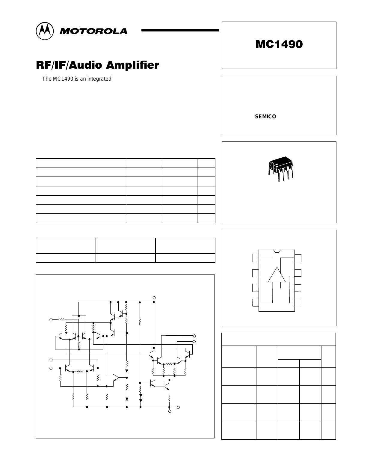
The MC1490 is an integrated circuit featuring wide–range AGC for use in
RF/IF amplifiers and audio amplifiers over the temperature range, –40° to
+85°C.
• High Power Gain:50 dB Typ at 10 MHz
45 dB Typ at 60 MHz
35 dB Typ at 100 MHz
• Wide Range AGC: 60 dB Min, DC to 60 MHz
• 6.0 V to 15 V Operation, Single Polarity Supply
• See MC1350D for Surface Mount
Order this document by MC1490/D
WIDEBAND AMPLIFIER
WITH AGC
SEMICONDUCTOR
TECHNICAL DATA
MAXIMUM RATINGS
Power Supply Voltage V
AGC Supply V
Input Differential Voltage V
Operating Temperature Range T
Storage Temperature Range T
Junction Temperature T
(TA = +25°C, unless otherwise noted.)
Rating Symbol Value Unit
CC
AGC
ID
A
stg
J
+18 Vdc
V
CC
5.0 Vdc
–40 to +85 °C
–65 to +150 °C
+150 °C
ORDERING INFORMATION
Device
MC1490P TA = –40° to +85°C Plastic
Operating
Temperature Range Package
Representative Schematic Diagram
2
V
CC
1.5 k
V
AGC
(–)
(+)
70
5
470
2.0 k
4
Inputs
6
66
5.0 k
1.1 k
Pins 3 and 7 should both be connected to circuit ground.
1.1 k
470
5.0 k
8.4 k
1.4 k
5.6 k
12.1 k5.5 k
2.8 k
1.9k
200
Substrate
45
200
7
200
3
2.8 k
Vdc
8
(+)
Outputs
(–)
1
8
1
P SUFFIX
PLASTIC PACKAGE
CASE 626
PIN CONNECTIONS
Output
1
(–)
2
V
CC
GND
Inverting
Parameter Symbol 30 60 Unit
Input
Reflection
Coefficient
Output
Reflection
Coefficient
Forward
Transmission
Coefficient
Reverse
Transmission
Coefficient
4
Input
SCATTERING PARAMETERS
(VCC = +12 Vdc, TA = +25°C, Zo = 50 Ω)
3
(Top View)
|S11|
θ11
|S22|
θ22
|S21|
θ21
S
12
θ12
–+
0.95
–7.3
0.99
–3.0
16.8
128
0.00048
84.9
8
7
6
5
f = MHz
Typ
Output
(+)
Substrate
Ground
Noninverting
Input
AGC
Input
0.93
–16–deg
0.98
–5.5–deg
14.7
64.3–deg
0.00092
79.2–deg
MOTOROLA ANALOG IC DEVICE DATA
Motorola, Inc. 1996 Rev 5
1
Page 2
MC1490
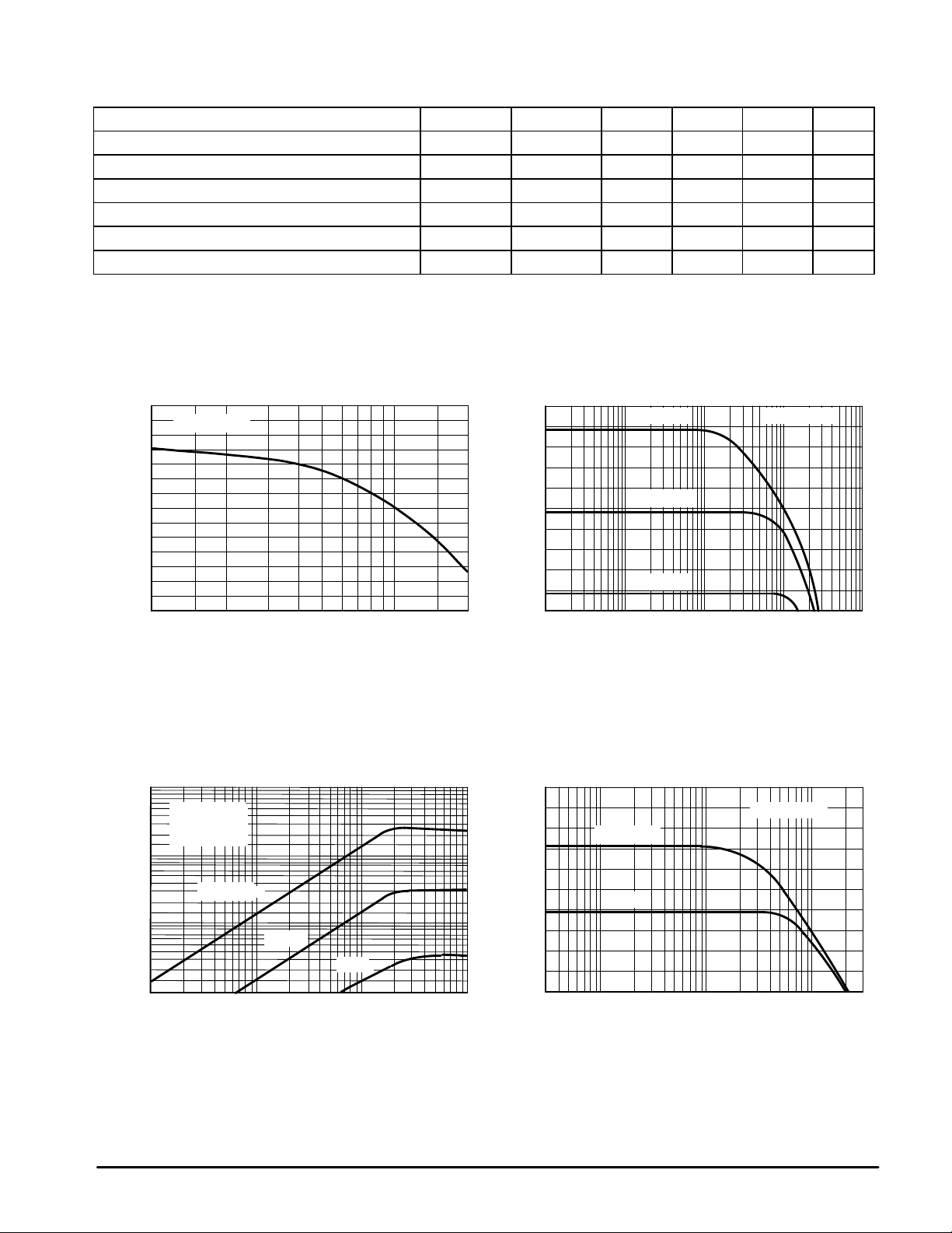
ELECTRICAL CHARACTERISTICS
Characteristic
Power Supply Current Drain – I
AGC Range (AGC) 5.0 V Min to 7.0 V Max 19 M
Output Stage Current (Sum of Pins 1 and 8) – I
Single–Ended Power Gain RS = RL = 50 Ω 19 G
Noise Figure RS = 50 Ohms 19 NF – 6.0 – dB
Power Dissipation – P
Figure 1. Unneutralized Power Gain versus
Frequency (T uned Amplifier, See Figure 19)
70
VCC = 12 Vdc
60
50
40
30
20
(SINGLE–ENDED OUTPUT)
, UNNEUTRALIZED GAIN (dB)
P
10
G
0
10
20 50 100 200
f, FREQUENCY (MHZ)
(VCC = 12 Vdc, f = 60 MHz, BW = 1.0 MHz, TA = 25°C)
Figure Symbol Min Typ Max Unit
CC
AGC
O
P
D
Figure 2. V oltage Gain versus Frequency
(Video Amplifier, See Figure 20)
50
40
30
20
10
, SINGLE–ENDED VOLTAGE GAIN (dB)
C
A
0
0.1 1.0 10 100 1000
– – 17 mA
–60 – – dB
4.0 – 7.5 mA
40 – – dB
– 168 204 mW
VCC = 12 VdcRL = 1.0 k
RL = 100
Ω
RL = 10
Ω
f, FREQUENCY (MHZ)
Figure 3. Dynamic Range: Output Voltage versus
Input V oltage (Video Amplifier, See Figure 20)
10
VCC = 12 Vdc
5.0
V
= 0 V
5(AGC)
f = 1.0 MHz
1.0
0.5
0.1
, OUTPUT VOLTAGE (V RMS)
0.05
O
V
0.01
0.1 0.2 0.5 1.0 2.0 5.0 10 20 50 100
RL = 1.0 k
100
Ω
en, INPUT VOLTAGE (mVRMS)
10
Ω
2
Figure 4. V oltage Gain versus Frequency
(Video Amplifier, See Figure 20)
50
VCC = 6.3 Vdc
40
30
20
10
, SINGLE VOLTAGE GAIN (dB)
V
A
0
0.3 0.5 1.0 3.0 5.0 10 30 50 100 300
RL = 1.0 k
100
Ω
Ω
f, FREQUENCY (MHZ)
MOTOROLA ANALOG IC DEVICE DATA
Page 3
MC1490
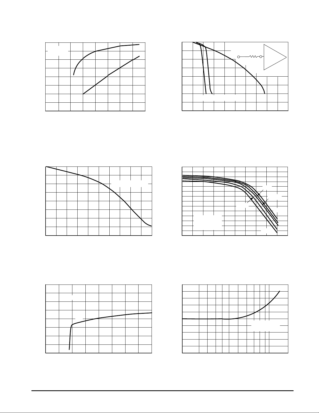
Figure 5. V oltage Gain and Supply Current versus
Supply V oltage (Video Amplifier, See Figure 20)
45
f = 1.0 MHz
40
Rl = 1.0
Ω
A
V
35
30
25
I
CC
20
15
10
, SINGLE–ENDED VOLTAGE GAIN (dB)
V
A
5.0
0 2.0 4.0 6.0 8.0 10 12 14 16
VCC, SUPPLY VOLTAGE (V)
Figure 7. T ypical Gain Reduction
versus AGC Current
0
10
20
100 < R
30
40
50
, GAIN REDUCTION (dB)
R
60
G
70
80
–40 –20 0 20 40 60 80 100 120 140 160
I
AGC CURRENT (µA)
AGC
AGC
< 100 k
24
21
18
15
12
9.0
6.0
3.0
0
Figure 6. T ypical Gain Reduction
versus AGC Voltage
0
10
20
V
R(AGC)
R
AGC
30
40
50
, GAIN REDUCTION (dB)
R
60
G
, SUPPLY CURRENT (mAdc)
C
I
70
R
AGC
= 0
R
= 5.6 k
Ω
AGC
Ω
80
0 3.0 6.0 9.0 12 15 18 21 24 27 30
V
AGC VOLTAGE (Vdc)
R(AGC),
Figure 8. Fixed T uned Power Gain Reduction versus
T emperature (See Test Circuit, Figure 19)
50
40
30
20
10
,POWER GAIN (dB)
0
p
G
–10
–20
5.0 5.2 5.4 5.6 5.8 6.0 6.2 6.4 6.6 6.8 7.0
VCC = 12 Vdc
f = 60 MHz
R
= 5.6 k
AGC
V
R(AGC),
Ω
+75°C
AGC VOLTAGE (Vdc)
5
R
AGC
0°C
+125°C
MC1490P
= 100 k
+25°C
–55°C
Ω
Figure 9. Power Gain versus Supply V oltage
(See T est Circuit, Figure 19)
80
70
60
f = 60 MHz
50
40
30
, POWER GAIN (dB)
p
20
G
G
P
10
0
0 2.0 4.0 6.0 8.0 10 12 14 16
VCC, POWER SUPPLY VOLTAGE (V)
MOTOROLA ANALOG IC DEVICE DATA
Figure 10. Noise Figure versus Frequency
10
9.0
8.0
7.0
6.0
5.0
4.0
3.0
NF, NOISE FIGURE (dB)
2.0
1.0
0
15 20 25 30 35 40 50 60 70 80 90 100
f, FREQUENCY (MHz)
RS Optimized
for minimum NF
150
3
Page 4

MC1490
Figure 11. Noise Figure versus
Source Resistance
20
18
VCC = 12 Vdc
16
14
12
10
8.0
6.0
NF, NOISE FIGURE (dB)
4.0
2.0
0
100 200 400 600 1.0 k 2.0 k 4.0 k 10 k
RS, SOURCE RESISTANCE (Ω)
f = 105 MHz
f = 60 MHz
f = 30 MHz
Figure 13. Harmonic Distortion versus AGC Gain
Reduction for AM Carrier (For Test Circuit, See Figure 14)
40
f = 10.7 MHz
Modulation: 90 % AM, fm = 1.0 kHz
35
Load at Pin 8 = 2.0 k
EO = peak–to–peak envelope of
30
modulated 10.7 MHz carrier at Pin 8
25
20
15
MODULA TION (%)
10
5.0
HARMONIC DISTORTION IN DETECTED
0
01020304050607080
40
35
30
25
20
15
NOISE FIGURE (dB)
10
5
0
Ω
EO = 2400 mVpp
GR, GAIN REDUCTION (dB)
Figure 12. Noise Figure versus
AGC Gain Reduction
f = 30 MHz
BW = 1.0 MHz
Test circuit has tuned input
providing a source resistance
optimized for best noise figure.
0 –10 –20 –30 –40 –50 –60 –70 –80
GR, GAIN REDUCTION (dB)
760 mVpp
240 mVpp
Figure 14. 10.7 MHz Amplifier Gain ] 55 dB, BW ] 100 kHz
6
5
MC1490P
4
3
7
36 pF
8
L2
1
RFC
2
L2 = 20 turns, #22 AWG wire
on a T12–44 micro metal
Toroid core (–100 pF)
MOTOROLA ANALOG IC DEVICE DATA
0.0020.002
50
Ω
Load
+12 Vdc
0.002
V
AGC
10.7 MHz
Ω
Source)
(50
L1 = 24 turns, #22 AWG wire
5.6 k
82 pF
50–150 pF
on a T12–44 micro metal
Toroid core (–124 pF)
L1
4
Page 5

MC1490
Figure 15. S11 and S22, Input and Output
Reflection Coefficient
Figure 16. S11 and S22, Input and Output
Reflection Coefficient
Figure 17. S21, Forward Transmission
Coefficient (Gain)
80 MHz
70 MHz
30 MHz
60 MHz
50 MHz
40 MHz
20 MHz
10 MHz
10
5.0
5.0
10
15
100 MHz
120 MHz
150 MHz
200 MHz
Figure 18. S12, Reverse Transmission
Coefficient (Feedback)
MOTOROLA ANALOG IC DEVICE DATA
5
Page 6

MC1490
Figure 19. 60 MHz Power Gain T est Circuit Figure 20. Video Amplifier
0.0001
µ
Input
(50
F
V
AGC
V
R(AGC)
6
5
4
C2
L1
Ω
)
C1
R
AGC
L1 = 7 turns, #20 AWG wire, 5/16″ Dia.,5/8″long
L2 = 6 turns, #14 AWG wire, 9/16
C1,C2,C3 = (1–30) pF
C4 = (1–10) pF
Shield
7
MC1490P
3
2
0.001
″
Dia.,3/4″long
Figure 21. 30 MHz Amplifier
(Power Gain = 50 dB, BW [ 1.0 MHz)
µ
F
0.002
(1 – 30) pF
Input
(50
Ω
)
38 pF
T1: Primary = 17 turns, #20 AWG wire on a Toroid core, (T44–6).
Secondary = 2 turns, #20 AWG wire.
L1
V
AGC
5.6 k
0.002 µF
V
R(AGC)
L1 = 12 turns, #22 AWG wire on a Toroid core,
(T37–6 micro metal or equiv).
6
5
4
7
MC1490P
3
8
1
2
1 – 10 pF
µ
10
+12 Vdc
C3
H
0.001
µ
µ
F
1.0
C4
Output
(50
Ω
8
L2
1
µ
F
)
+12 Vdc
V
R(AGC)
V
R(AGC)
10 k
5.6 k
1.0
e
i
0.001
F
7
6
µ
MC1490P
F
5
4
3
µ
F
2
1.0 µF
0.001
8
1
µ
F
e
o
R
L
+12 Vdc
Figure 22. 100 MHz Mixer
V
6.0 V
C2
T1
RL = 50
Ω
Input from
local oscillator
(70 MHz)
Signal Input
(100 MHz)
(1 – 30) pF
AGC
7
L1
0.002
5
6
4
3
µ
MC1490P
2
F
0.002 µF
″
, ID Dia., 5/8″ long
8
1
100
(1 – 10) pF
L1 = 5 turns, #16 AWG wire, 1/4
L2 = 16 turns, #20 AWG wire on a Toroid core, (T44–6).
L2
(1 – 10) pF
(1 – 30) pF
IF Output
(30 MHz)
+12 Vdc
10
µ
H
Figure 23. Two–Stage 60 MHz IF Amplifier (Power Gain [ 80 dB, BW [ 1.5 MHz)
V
R(AGC)
5.1 k
Input
(50
T1: Primary Winding = 15 turns, #22 AWG wire, 1/4″ ID Air Core
24 pF
Ω
)
200 µH
(1–10) pF
µ
F
0.002
Secondary Winding = 4 turns, #22 AWG wire,
Coefficient of Coupling [ 1.0
4
5
6
+12 Vdc
Shield
7
8
MC1490P MC1490P
(1–10) pF
1
2
3
RFC
10
µ
H
6
10 k
(1–10) pF
T1
1.0 k
Shield
0.002
µ
F
39 pF
0.002
T2: Primary Winding = 10 turns, #22 AWG wire, 1/4″ ID Air Core
Secondary Winding = 2 turns, #22 AWG wire,
Coefficient of Coupling [ 1.0
7
4
5
6
3
µ
F
8
(1–10) pF
1
2
0.001 µF
RFC
T2
Output
(50
MOTOROLA ANALOG IC DEVICE DATA
Ω
)
Page 7

DESCRIPTION OF SPEECH COMPRESSOR
F
MC1490
T able 1. Distortion versus Frequency
The amplifier drives the base of a PNP transistor operating
common–emitter with a voltage gain of approximately 20.
The control R1 varies the quiescent Q point of this transistor
so that varying amounts of signal exceed the level Vr. Diode
D1 rectifies the positive peaks of Q1’s output only when these
peaks are greater than Vr ] 7.0 V. The resulting output is
filtered by Cx, Rx.
Rx controls the charging time constant or attack time. Cx is
involved in both charge and discharge. R2 (the 150 kΩ and
input resistance of the emitter–follower Q2) controls the
decay time. Making the decay long and attack short is
accomplished by making Rx small and R2 large. (A
Darlington emitter–follower may be needed if extremely slow
decay times are required.)
The emitter–follower Q2 drives the AGC Pin 5 of the
MC1490P and reduces the gain. R3 controls the slope of
signal compression.
Figure 24. Speech Compressor
+12 V
requency
100 Hz 3.5% 12% 15% 27%
300 Hz 2% 10% 6% 20%
1.0 kHz 1.5% 8% 3% 9%
10 kHz 1.5% 8% 1% 3%
100 kHz 1.5% 8% 1% 3%
Notes: (1) Decay = 300 ms (3) Decay = 20 ms
(2) Cx = 7.5 µF (4) Cx = 0.68 µF
25 µF
0.001
1.0 k
Distortion Distortion
10 mV ei100 mV ei10 mV ei100 mV e
Notes 1 and 2 Notes 3 and 4
Attack = 20 ms Attack = 3.0 ms
Rx = 0 (Short) Rx = 1.5 kΩ
i
Input
R3
15 k
15
µ
F
15
+12 V
Q2
2N3904
4.7 k 150 k
1.0 k
2.2 k220
33 k
R1
100 k
+12 V+12 V
10 µF
10
µ
Output
F
V
r
2
5
4
6
µ
F
MC1490P
7
R2
R
C
x
1
x
8
3
Q1
2N3906
D1
6.8 k
MOTOROLA ANALOG IC DEVICE DATA
7
Page 8

NOTE 2
–T–
SEATING
PLANE
H
58
–B–
14
F
–A–
C
N
D
K
G
0.13 (0.005) B
M
T
MC1490
OUTLINE DIMENSIONS
P SUFFIX
PLASTIC PACKAGE
CASE 626–05
ISSUE K
L
J
M
M
A
M
NOTES:
1. DIMENSION L TO CENTER OF LEAD WHEN
FORMED PARALLEL.
2. PACKAGE CONTOUR OPTIONAL (ROUND OR
SQUARE CORNERS).
3. DIMENSIONING AND TOLERANCING PER ANSI
Y14.5M, 1982.
DIM MIN MAX MIN MAX
A 9.40 10.16 0.370 0.400
B 6.10 6.60 0.240 0.260
C 3.94 4.45 0.155 0.175
D 0.38 0.51 0.015 0.020
F 1.02 1.78 0.040 0.070
G 2.54 BSC 0.100 BSC
H 0.76 1.27 0.030 0.050
J 0.20 0.30 0.008 0.012
K 2.92 3.43 0.115 0.135
L 7.62 BSC 0.300 BSC
M ––– 10 ––– 10
N 0.76 1.01 0.030 0.040
INCHESMILLIMETERS
__
Motorola reserves the right to make changes without further notice to any products herein. Motorola makes no warranty , representation or guarantee regarding
the suitability of its products for any particular purpose, nor does Motorola assume any liability arising out of the application or use of any product or circuit, and
specifically disclaims any and all liability, including without limitation consequential or incidental damages. “T ypical” parameters which may be provided in Motorola
data sheets and/or specifications can and do vary in different applications and actual performance may vary over time. All operating parameters, including “Typicals”
must be validated for each customer application by customer’s technical experts. Motorola does not convey any license under its patent rights nor the rights of
others. Motorola products are not designed, intended, or authorized for use as components in systems intended for surgical implant into the body, or other
applications intended to support or sustain life, or for any other application in which the failure of the Motorola product could create a situation where personal injury
or death may occur. Should Buyer purchase or use Motorola products for any such unintended or unauthorized application, Buyer shall indemnify and hold Motorola
and its officers, employees, subsidiaries, affiliates, and distributors harmless against all claims, costs, damages, and expenses, and reasonable attorney fees
arising out of, directly or indirectly, any claim of personal injury or death associated with such unintended or unauthorized use, even if such claim alleges that
Motorola was negligent regarding the design or manufacture of the part. Motorola and are registered trademarks of Motorola, Inc. Motorola, Inc. is an Equal
Opportunity/Affirmative Action Employer.
How to reach us:
USA/EUROPE/ Locations Not Listed: Motorola Literature Distribution; JAPAN: Nippon Motorola Ltd.; Tatsumi–SPD–JLDC, 6F Seibu–Butsuryu–Center,
P.O. Box 20912; Phoenix, Arizona 85036. 1–800–441–2447 or 602–303–5454 3–14–2 Tatsumi Koto–Ku, Tokyo 135, Japan. 03–81–3521–8315
MFAX: RMF AX0@email.sps.mot.com – TOUCHT ONE 602–244–6609 ASIA/PACIFIC: Motorola Semiconductors H.K. Ltd.; 8B Tai Ping Industrial Park,
INTERNET: http://Design–NET.com 51 Ting Kok Road, Tai Po, N.T., Hong Kong. 852–26629298
8
◊
MOTOROLA ANALOG IC DEVICE DATA
MC1490/D
*MC1490/D*
 Loading...