

Page 1
MC1489
■ INPUTRESISTANCE–3kto7kΩ
■ INPUTSIGNALRANGE– ± 30V
■
INPUTTHRESHOLDHYSTERESISBUILT-IN
■ RESPONSECONTR OL:
a) LOGICTHRESHOLDSHIFTING
b) INPUT NOISEFILTERING
DESCRIPTION
The MC1489 monolithic quad line receivers are
designed to interface data therminal equipment
with data communications equipment in
conformance with the specifications of EIA
StandardNo. RS-232C.
MC1489A
QUAD LINE RECEIVERS
P
DIP14
( Plastic)
D
SO14
(PlacticMicropackage)
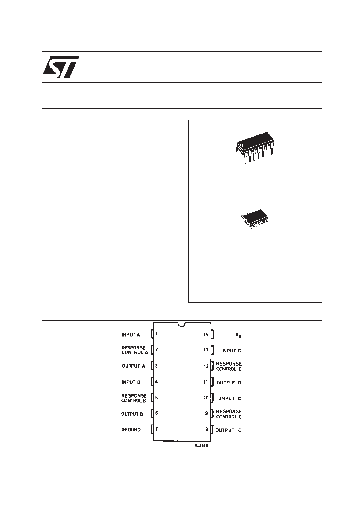
PIN CONNECTION
ORDERCODES:
MC1489P,MC1489AP(DIP–14 Plastic)
MC1489D,MC1489AD(SO-14)
(topview)
March 2000
1/10
Page 2
MC1489 / MC1489A
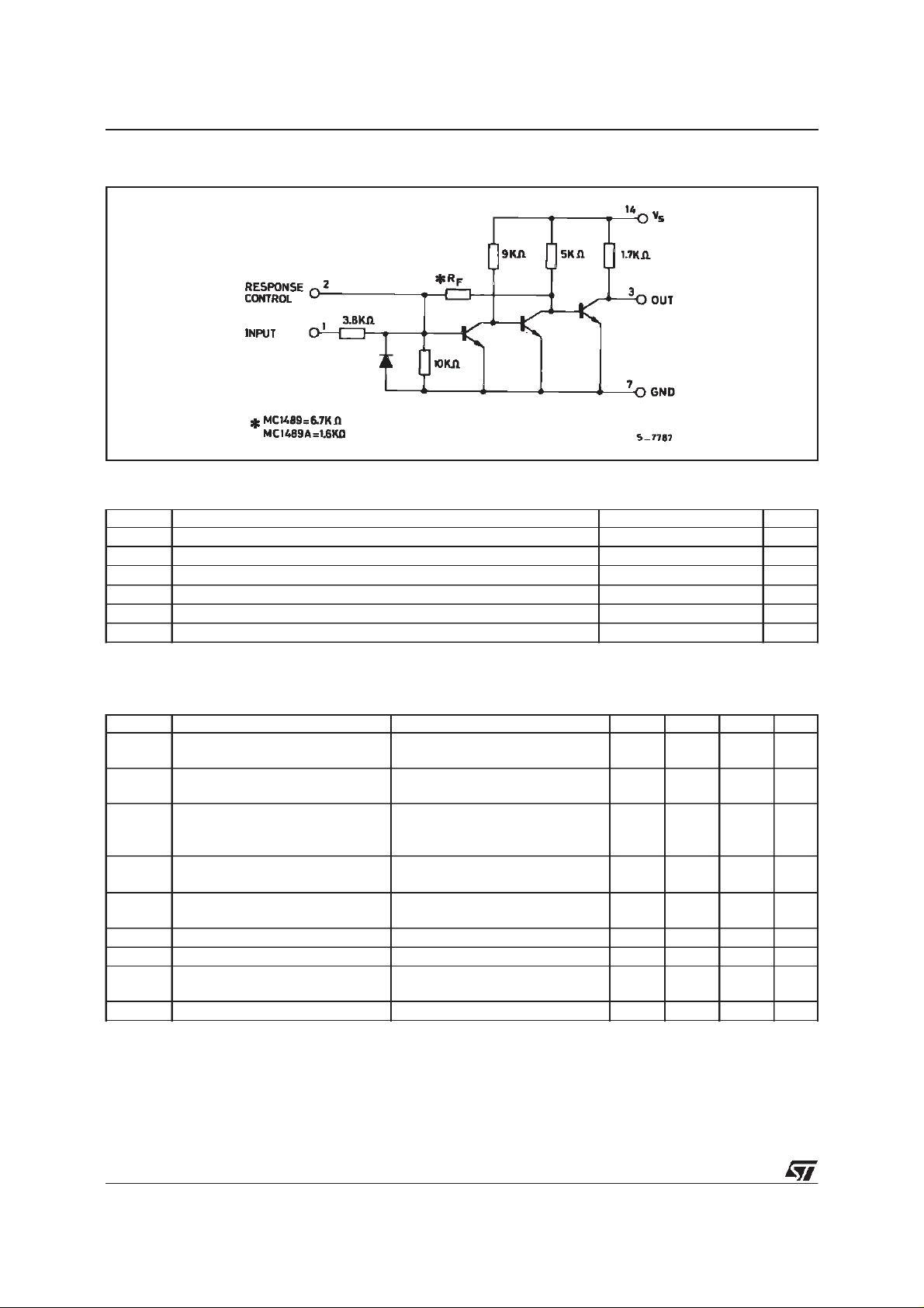
SCHEMATIC DIAGRAM (1/4 of circuit shown)
ABSOLUTE MAXIMUM RATINGS
Symb ol Parameter Value Unit
V
Power Supply Voltage 10 V
S
V
Input Voltage Range
I
I
Output Load Current 20 mA
OL
P
Power Dissipation 1 W
tot
T
Operating Ambient Temperature 0 to 75
amb
T
Storage Temperature Range –65 to 150
stg
30 V
±
o
C
o
C
ELECTRICAL CHARACTERISTICS
ResponseControl Pin is Open ; V
= 5 V,T
S
Symb ol Parameter Test Cond t i ons Mi n . Typ . Max. Unit
Positive Input Current VIH=25V
I
IH
I
Negative Input Current VIL=_25V
IL
V
Input Turn-on Threshold Voltage
IH
V
Input Turn-off Threshold Voltage
IL
V
V
Ouptut Voltage High VIH= 0.75V, IL=-0.5mA
OH
Output Voltage Low VIL= 3V, IL= 10mA 0.2 0.45 V
OL
I
Output Short Circuit Current
OS
I
Power Supply Current All gates ”on”, Io=0mA
S
P
Power Consumption VIH= 5V 80 130 mW
C
= 0 to 75oC, unless otherwise specified
amb
3.6
V
IH
=3V
0.43
-3.6
V
=_3V
IL
=25oC, V
T
amb
= 10mA for MC1489
I
L
OL
0.45
≤
forMC1489A
=25oC, V
T
amb
I
= -0.5mA
L
= 0.5mA Input Open Circuit
I
L
V
=5V 16 26
IH
OL
2.5V
≥
-0.43
1
1.75 1.95
0.75 1.25
2.5
2.5
4
4
_
3
8.3 mA
-8.3 mA
1.5
2.25
5
5
_
4mA
mA
V
V
V
2/10
Page 3
MC1489 / MC1489A
SWITCHING CHARACTERISTICS
= 5V,T
V
S
Symbol Parameter Test Condtions Min. Typ. Max. Unit
t
PLH
t
TLH
t
PHL
t
THL
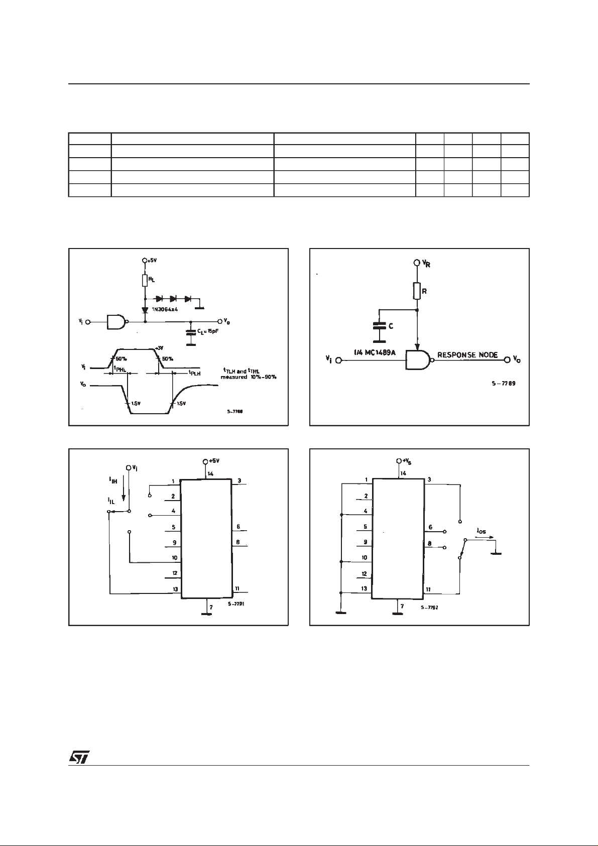
TESTCIRCUITS
Figure1 :
=25oC, see Figure1
amb
Propagation delay Time
Rise Time
Propagation Delay Time
Fall Time
Switching Response
R
R
R
R
=3.9k
L
L
L
L
Ω
=3.9k
Ω
=390
Ω
=390
Ω 10 20 ns
Figure2 :
ResponseControl Node
25 85 ns
120 175 ns
25 50 ns
Figure3 :
Input Current
Figure4 :
C: capacitor is fornoisefiltering
OutputShort-CircuitCurrent
3/10
Page 4

MC1489 / MC1489A
Figure5 :OutputVoltage and Input Threshold
Voltage
TYPICALAPPLICATION: RS232CData Transmission
Figure6 :Power Supply Current
4/10
Page 5

MC1489 / MC1489A
TYPICALCHARACTERISTICS
V
= 5V,T
S
Figure7 :Input Current Figure8 :MC1489Input ThresholdVoltage
=25oC, unlessotherwisespecified
amb
Adjustment
Figure9 :MC1489A Input ThresholdVoltage
Adjustment
Figure11 :
InputThreshold versusPower Supply
Voltag
Figure10 :InputThreshold versus Temperature
5/10
Page 6

MC1489 / MC1489A
APPLICATION INFORMATION
GENERAL INFORMATION
The Electronic Industries Association (EIA) has
released the RS-232C specification detailing the
requirements for the interface between data
processing equipment and data communications
equipment. This standard specifies not only the
number and type of interface leads, but also the
voltage levels to be used. The MC1488 quad
driver and its companion circuit, the MC1489
quad receiver, provide a complete interface
system between DTL or TTL logic levels and the
RS-232C defined levels. The RS-232C
requirements as applied to receivers are
discussedherein.
The required input impedance is defined as
between 3000Ω and 7000Ω for input voltages
between 3.0 and 25V in magnitude ; and any
voltage on the receiver input in an open circuit
condition must be less than 2.0V in magnitude.
The MC1489 circuits meet these requirements
witha maximum open circuitvoltage of one V
The receiver shall detect a voltage between - 3.0
and - 25V as a Logic ”1” and inputs between +
3.0 and + 2.5V as a Logic ”0”. On some
interchangeleads, an open circuit of power ”OFF”
condition (300Ω or more to ground) shall be
decoded as an ”OFF” condition or Logic ”1”. For
the reason, the input hysteresis thresholds of the
MC1489 circuits are all above ground. Thus an
open or grounded input will cause the same
output as a negativeor Logic ”1” input.
DEVICECHARACTERISTICS
The MC1489 interface receivers have internal
feedback from the second stage to the input
stage providing input hysteresis for noise
BE
rejection. The MC1489 input has typical turn-on
voltage of 1.25Vand turn-off of 1.0 V for a typical
hysteresis of 250mV. The MC1489A has typical
turn-on of 1.95V and turn-off of 0.8V for typically
1.15V of hysteresis.
Each receiver section has an external response
control node in addition to the input and output
pins, thereby allowing the designer to vary the
input threshold voltage levels. A resistor can be
connected between this node and and an
external power supply. Figures 2, 4 and 5
illustratethe inputthreshold voltage shiftpossible through this technique.
This response node can also be used for the
filtering of the high-frequency, high-energy noise
pulses. Figures 8 and 9 show typical noise-pulse
rejection for externalcapacitors of various sizes.
These two operations on the response node can
be combined or used individually for may
combinations of interfacing applications. The
MC1489 circuits are particularly useful for
.
interfacing between MOS circuits and
MDTL/MTTL logic systems. In this application,
the input threshold voltages are adjusted. (with
the appropiate supply and resistor values) to fall
in the center of the MOS voltage logic levels (see
Figure 10).
The response node may also be used as the
receiver input as long as the designer realizes
that he may not drive this node with a low
impedance source to a voltage greater than one
diode above ground or less than one diodebelow
ground. This feature is demonstrated in Figure 11
where two receivers are slaved to the same line
that must still meet the RS-232C impedance
requirement.
6/10
Page 7

MC1489 / MC1489A
Figure12 :TypicalTurn-on Therhold versus
Capacitancefrom Response Control
Pinto GND
Figure 13 :TypicalTurn-on Therholdversus
Capacitancefrom Response Control
Pin to GND
Figure14 : TypicalParallelingof Two MC1489/AReceiversto Meet RS-232C
7/10
Page 8

MC1489 / MC1489A
Plastic DIP-14 MECHANICAL DATA
DIM.
MIN. TYP. MAX. MIN. TYP. MAX.
a1 0.51 0.020
B 1.39 1.65 0.055 0.065
b 0.5 0.020
b1 0.25 0.010
D 20 0.787
E 8.5 0.335
e 2.54 0.100
e3 15.24 0.600
F 7.1 0.280
I 5.1 0.201
L 3.3 0.130
Z 1.27 2.54 0.050 0.100
mm inch
8/10
P001A
Page 9

SO-14 MECHANICALDATA
MC1489 / MC1489A
DIM.
MIN. TYP. MAX. MIN. TYP. MAX.
A 1.75 0.068
a1 0.1 0.2 0.003 0.007
a2 1.65 0.064
b 0.35 0.46 0.013 0.018
b1 0.19 0.25 0.007 0.010
C 0.5 0.019
c1 45 (typ.)
D 8.55 8.75 0.336 0.344
E 5.8 6.2 0.228 0.244
e 1.27 0.050
e3 7.62 0.300
F 3.8 4.0 0.149 0.157
G 4.6 5.3 0.181 0.208
L 0.5 1.27 0.019 0.050
M 0.68 0.026
S 8 (max.)
mm inch
P013G
9/10
Page 10

MC1489 / MC1489A
Information furnished isbelieved tobe accurate andreliable. However, STMicroelectronics assumes no responsibility forthe consequences
of use of such information nor for any infringement of patents or other rights of third parties which may result from its use. No license is
granted by implication or otherwise under any patent or patent rights of STMicroelectronics. Specification mentioned in this publication are
subject tochange withoutnotice. This publication supersedes and replaces allinformation previously supplied. STMicroelectronics products
are not authorized for use as critical components in lifesupport devices or systems withoutexpress written approval of STMicroelectronics.
The ST logo is a registeredtrademark of STMicroelectronics
2000 STMicroelectronics – Printed in Italy – All Rights Reserved
STMicroelectronics GROUP OF COMPANIES
Australia - Brazil - China - Finland -France - Germany - Hong Kong - India - Italy - Japan- Malaysia - Malta - Morocco
Singapore - Spain- Sweden - Switzerland - UnitedKingdom - U.S.A.
http://www.st.com
.
10/10
 Loading...