

Page 1
I
Advance Information
I I
REAL-TIME CLOCK PLUS RAM (RTC)
The MC146818A Real-Time Clock plus RAM is a peripheral device
which includes the unique MOTEL concept for use with various
microprocessors, microcomputers, and larger computers. This part
combines three unique features: a complete time-of-day clock with
alarm and one hundred year calendar, a programmable periodic interrupt and square-wave generator, and 50 bytes of low-power static
RAM. The MC146818A uses high-speed CMOS technology to interface
with 1 MHz processor buses, while consuming very little power.
The Real-Time Clock plus RAM has two distinct uses. First, it is
designed as a battery powered CMOS part (in an otherwise NMOS/TTL
system) including all the common battery backed-up functions such as
RAM, time, and calendar. Secondly, the MC146818A maybe used with
a CMOS microprocessor to relieve the software of the timekeeping ,~~
workload and to extend the available RAM of an MPU such as the ., “’~:$
MC146805E2.
,!!:\’;
.\,i,.,..
. ....
● Low-Power, High-Speed CMOS
~\}t
,.,.>*t!F\+{k
,1,
$s,,..
● Internal Time Base and Oscillator
~;, ~p
)>.
~$$~.
‘,&Q.%~!*
O Counts Seconds, Minutes, and Hours of the Day
*>sq,.,,\,$4:*,
$+.~:;;,. ..~.
“’t:>?,.
● Counts Days of the Week, Date, Month, and Year ,$:
;<4 ,
● 3 V to 6 V Operation
..!.*:,:
~t.k,$,.,
● Time Base Input Options: 4.194304 MHz, 1.048ti ~~z, or 32.7W
kHz
,,,,,,M,,)$f,
<..%.-...*<.*$,
,$\ \.,
,,:,,
. ..i,;t~
● Time Base Oscillator for Parallel Resonan~$$~{S]s
.~;\l...
● 40 to 200 pW Typical Operating Power{,~L:~#~ ‘Frequency Time Base
● 4.0 to 20 mW Typical Operating Po.~%j~*$?gh Frequency Time Base
,~$.~,,,
● Binary or BCD Representation ~fTW~ Calendar, and Alarm
● 12- or 24-Hour Clock with A~$oQ$PM in 12-Hour Mode
.$k,..?.l,{+<,,$$,>:,.,
● Daylight Savings Time OplWn ‘$
*;* $*,,$$
● Automatic End of Mo~:~’’~$e6gnition
● Automatic Leap Y~r ~&&~ensation
● Microprocessor#$@t@mpatible
~‘.$$*$
● Selectable Ba$W&n’Wotorola and Competitor Bus Timing
, -~.,y,}$~*
● Multiplex@:~@ fbr Pin Efficiency
~’.,-,,
● lnterfq&$&%@% Software as 64 RAM Locations
● 14 B~es:$’~CIOck and Control Registers
,,*J
● ~’~~~~$i’of General Purpose RAM
....~.
@x;.$J&%wsBit indicates Data Integrity
?{&us Compatible Interrupt Signals (~Q)
..
● Three Interrupts are Separately Software Maskable and Testable
Time-of-Day Alarm, Once-per-Second to Once-per-Day
Periodic Rates from 30.5 ps to 500 ms
End-of-Clock Update Cycle
● Programmable Square-Wave Output Signal
● Clock Output May Be Used as Microprocessor Clock Input
At Time Base Frequency -1 or +4
● 24-Pin Dual-In-Line Package
● Quad Pack Also Available
.
hls document contains !ntormatlon on a new product. Specltlcatlons and tntormatlon here!n
MC146818A
CMOS \
CASE 623
u“
I
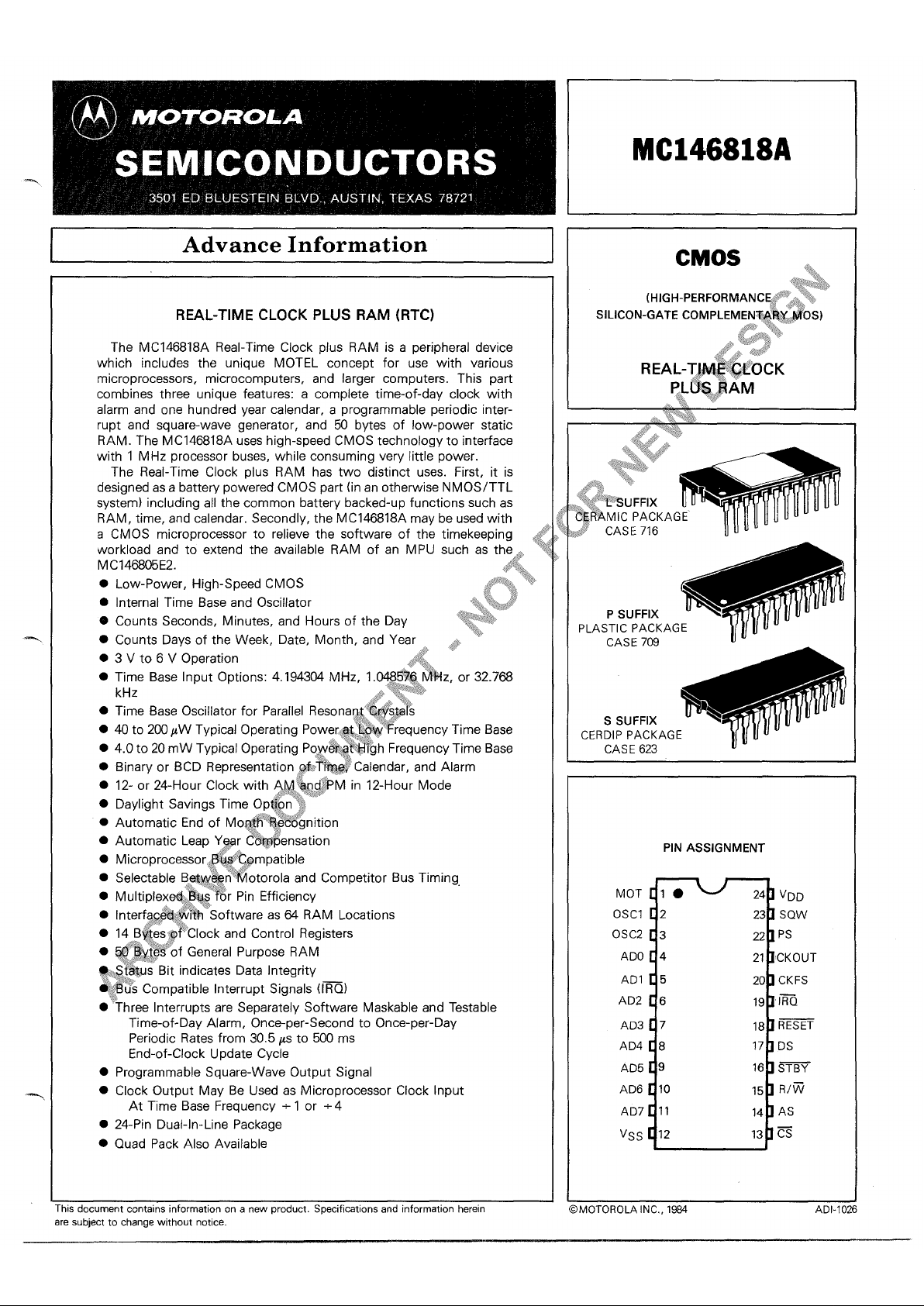
PIN ASSIGNMENT
‘oT ~vDD
Oscl [ 2
23 ] SQW
0SC2 [ 3 22 ] Ps
ADO [ 4
21 JCKOUT
AD1 [ 5
20 ] CKFS
AD2 [ 6
lg ] l~Q
AD3 [ 7
18 ] RESET
AD4 [ 8
17 ] DS
AD5 c g
16 ] STBY
AD6 [ 10
15 ] Rl~
AD7 [ 11 14 ] AS
Vss [
12
13 ]=
)MOTOROLAINC,, lW
ADI-1026
are subject to change without notice
Page 2
FIGURE 1 – BLOCK DIAGRAM
Clock
~ CKOUT
+
output
~ CKFS
v
Storage Temperature Range
Tstg
–55to +150
Oc
THERMAL CHARACTERISTICS
Characteristic
Symbol I
Value Unit
User RAM
(50 Bytes)
sow
~Q
RESET
Ps
,i,>,~
.. ~><.,
,*
.*$:, \ h .
~:*.
. ..
?+
$.;).,,<,:?
,’<;}.:-
MAXIMUM RATINQ~~(@oJjages referenced to VSS)
R~$n& “~:?’
Symbol Value
Unit
Supply Volta~J** “ ‘$?
VDD –0.3 to +8.0
v
All Input V:$~&.~xcept OSC1
Vin V5S– O.5 to VDD+O.5
v
Current ~rai~~r Pin Excluding
Vmi,a%q,.vs s
I 10
mA
This device contains circuitry to protect the in-
Op&~~~&Temperature Range
puts against damage due to high static voltages
TL to TH
or electric fields; however, it is advised that nor-
‘~%$~6818A
0 to 70
‘<@c146818AC
mal precautions be taken to avoid application of
TA
– 40 to 85
Oc
any voltage higher than maximum rated voltages
to this high-impedance circuit. For proper operation it is recommended that Vin and Vout be constrained to the range VSS =(Vin or Voutl
s VDD. Reliability of operation is enhanced if
unused inputs are tied to an appropriate logic
voltage level (e.g., either VSS or VDD).
Thermal Resistance
Plastic
I I
120
I I
Cerdlp 9JA
65 “c/w
Ceramic
50
@
MOTOROLA Semiconductor Products Inc.
2
—
—
Page 3
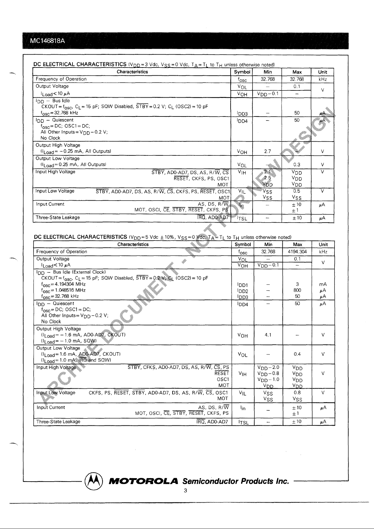
)C ELECTRICAL CHARACTERISTICS (vD
D= 3
Vdc, vs s = O Vdc, TA = Tl to TH unless otherwise noted)
Characteristics
I Symbol I Min
I
Max
I
Unit
I
Frequency of Operation
fosc
32.768 32.768
kHz
Output Voltage vOL
—
0.1
lLoad< lOpA vOH
v
VDD– O.1 –
IDD – Bus Idle
CKOUT=fosc, CL= 15 pF; SOW Disabled, STBY=O.2 V; CL (OSC2)= 10 pF
fosc=32.76B kHz
.\,
IDD3 –
50
A&fi%$k
IDD – Quiescent
IDD4 –
50
“~{?.
fosc= DC; OSC1 = DC;
$“’:#$, !,
~~.+,,~i:”
All Other
lnpUtS=vDD–0.2 V;
:,.:,.~
~+,,....
. .:s.‘ ..
NO Clock
i,,..
..,t>.$.‘:.*$
\k;~#\ ~,
....,.
Output High Voltege
.,+ ..%)$
i’t” *
(lLoad= – 0.25 mA, All Outputs)
~-.>,,->,,.,/,
vOH
2.7 t+?’+’~’’t;;k~ v
Output Low Voltage
?J
<t~tl,
(iLoad= 0.25 mA, All
OUtpUtS)
,,} \k*t
VOL
$i.,,,,
-$.*;,,’:,: ~
0.3 v
Input High Voltage
——
STBY, ADO-AD7, DS, AS, R/W, CS
vlH
, %&$$y’
VDD v
RESET, CKFS, PS, OSC1
.,$,@,q.,
VDD
‘$:?y$:~ ~?:,
MOT
,,. ‘k$,’w.~’D
VDD
Input Low Voltage
——
~, ADO-AD7, DS, AS, R/W, CS, CKFS, PS, RESET, OSCI
vlL ‘?$yvss
0.5 v
MOT .#vj
Vss
Vss
Input Current
AS, DS, R/~F
~~:$~
–
* 10
—— —
PA
MOT, OSCI, CE, STBY, RESET, CKFS, ,P# ‘$ ‘“
*I
Three-State Leakage IRQ, AD@@fl~lTsL –
* 10 WA
.::.
Input Current
AS, DS, R/~
Iin
I I
+10 AA
—— —
MOT, OSCI, CE, STBY, RESET, CKFS, PS
—
*1
I
1 1
, I
Three-State Leakage IRQ, ADO-AD7 ITSL I –
*IO
PA
1
m
MOTOROkA Semiconductor Products Inc.
3
Page 4
BUS TIMING
VDD=5.O V
*lo%
Vnn=3.O V
1 TTL and
Ident.
ti;F Load
130 pF Load
Number
Characteristi~ Symbol
Min Max Min Max Unit
1 Cycle Time
tcvc
5000 –
953 dc
ns
2 Pulse Width, DS/E Low or ~D/WR High PWEL lm
—
300 –
ns
3——Pulse Width, DS/E High or RD/WR Low PWEH 15m
—
325 –
ns
4 Input Rise and Fall Time tr, tf
—
100
—
30
ns
8 R/~ Hold Time tRWH 10 – 10 – ns “~$
13 R/~ Setup Time Before DS/E
,:,,,
tRWS 2m –
80
*.#*..,...,:{
—
~s %+.<
.$..
14 Chip Select Setup Time Before DS, ~R, or ~D tcs
200 –
,,.
25
—
~: m
15
Chip Select Hold Time
tCH 10
—
o
—
,,~r$
~~~;~e.:
18 Read Data Hold Time tDHR 10
Im
10
21 Write Data Hold Time
tnu\A/ 100 – o
SI24
Muxed Address Valid Time to AS/ALE Fall
I
tASL 2~ –
I
50 ,~p+:;a “’
I
n:
25 I Muxed Address Hold Time tAHL 100 I –
w “t “-
~*... ..s..’
~y>>,
ns
I
—
26
DelaV Time DS/E to AS/ALE Rise
tASD m –
, ‘* ‘ .- ns
27 Pulse Width, AS/ALE High
pwAs H
6~
– *,i$
;~J$$95
—
ns
28
DelaV Time, AS/ALE to DS/E Rise
tASED 500
* %:.\tf.,:/?@
ax..,.!>.
—
ns
30
Peripheral Output Data Delay Time from DS/ E or ~ tDDR 1300
.,~.,.,.?~...‘,’!..~,~
‘.?.?~i~,.~,:,
20 240
ns
31
Peripheral Data Setup Time tDSW 1q$.ii ~. ~’ 2m – ns
32
S~ Setup Time before AS/ALE Rise
tSBS
~Q:@:J~$+’3’–
TBD –
33
S~ Hold Time after AS/ALE Fall
tSBH
$~B~~ ~ _
TBD –
NOTE: Designations E, ALE, ~, and ~R refer to signals from alternative Mp;cessor signals.
.,.. ....
* Refer to IMPORTANT NOTICES appearing on page 20 of this data :~~t, .
‘~+.k
.,
Note: VHIGH=VDD–2.O
V, VLOW=O.8 V, for VDD=5.O V +IOYO for outputs only.
VHIGH=2.O V, VLOW=O.5 V,
for VDD=3.O V for outputs onlv.
@
MOTOROLA Semiconductor Products Inc.
4
—
-.
Page 5
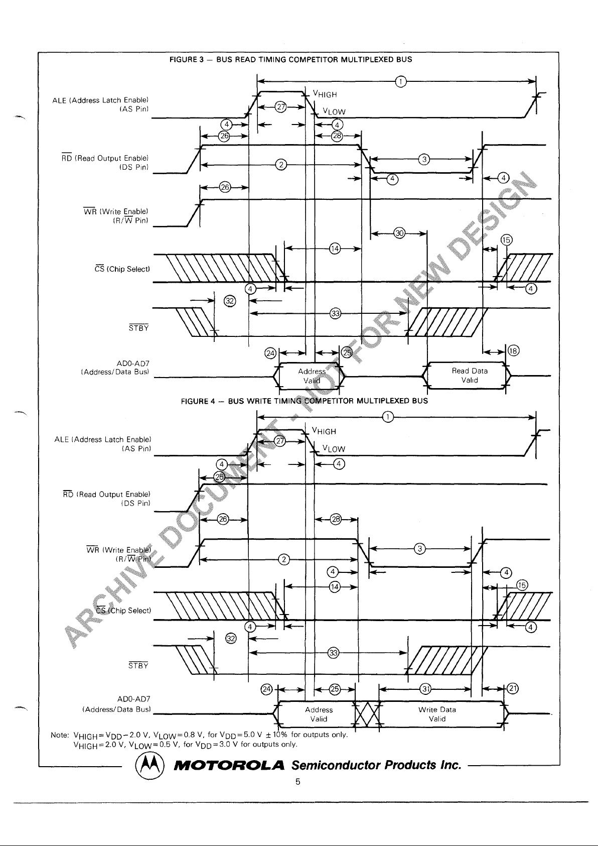
FIGURE 3 – BUS READ TIMING COMPETITOR MULTIPLEXED BUS
‘LE(AddressLatch
~ (Read Output Enable)
(DS Pin)
I IL
C= (Chip Select)
STBY
ADO-AD7
(Address/ Data Bus)
FIGURE 4 – BUS WRITE TIMINti?@PETITOR MULTIPLEXED BUS
@- *W
25 . 31
< ;
‘-
J
A
@
ADO-AD7
(Address/ Data
Bus) Address Write Data
Valid Valld
Note: VHIGH=VDD-2.O V, VLOW=O.8 V, for VDD=5.O V A 10% for outputs only.
VHIGH=2.O V, VLOW=O.5 V, for VDD=3.O V for outputs only.
@
MOTOROLA Semiconductor Products Inc.
5
Page 6
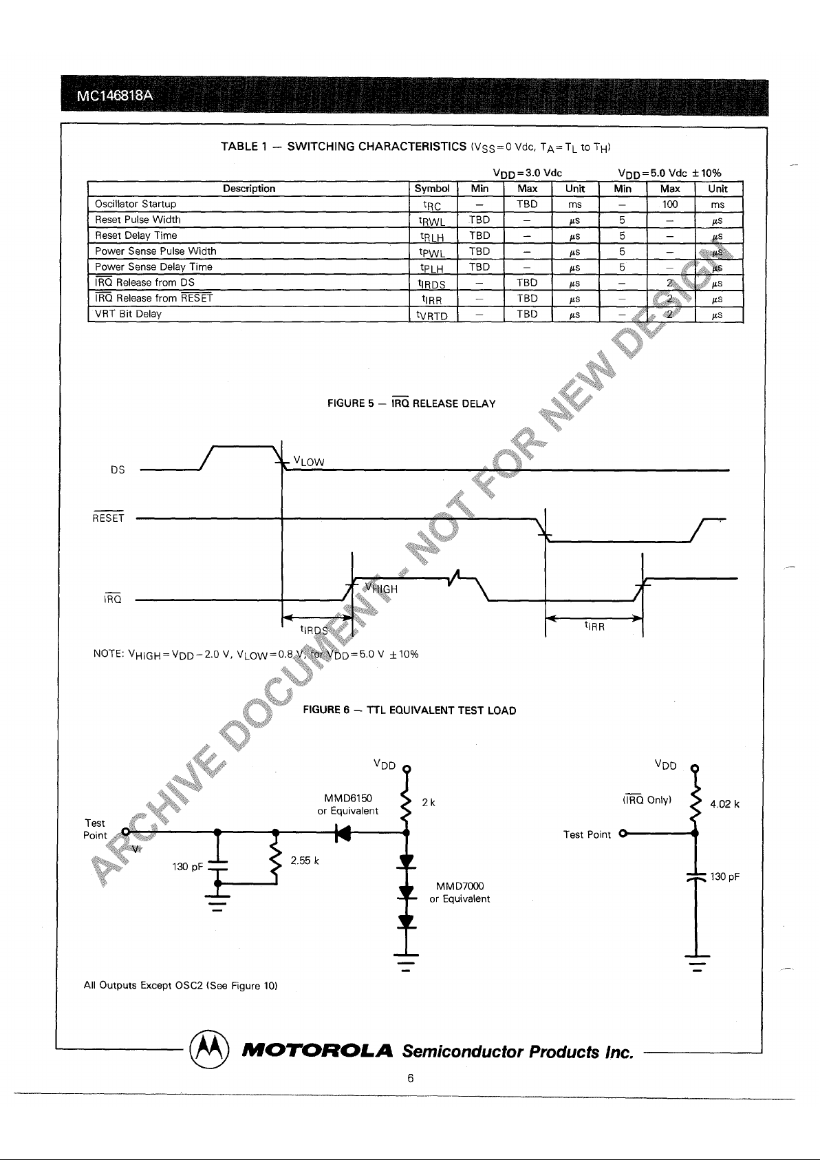
TABLE 1 – SWITCHING CHARACTERISTICS (VSS=O Vdc, TA= TL to TH)
VDD=3.O Vdc
VDD = 5.0 Vdc & 10”A
I
Description I SymbolIMin
I
Max
I
Unit
I
Min
I
Max
I
Unit
I Oscillator Startu~
ltRrl– lTBDlms]– ll~lmsl
1
Reset Pulse Width
I
tRWL[TBD
I
—
I
KS
I
51–
I
ps
I
Reset Delay Time
tRLH
I
TBD I –
I
ps
I
51–
&s
DA,.,-.
C---- D, ,1-- !AI; A+L I +-, .,, TDn I ..- C I I ‘i\!
DS
RESET
ITQ
.
All Outputs Except OSC2 (See Figure 10)
2k
MM D7000
or Equivalent
.
VDD
(KQ OnIV)
T
L 130pF
m
MOTOROLA Semiconductor Products Inc.
6
-.
.—
.—
—
Page 7

VDD Pin
RESET Pin
CKOUT Pin
VDD Pin
Ov
PS Pin .
Ov
FIGURE 7 – POWER-UP
~~
~ The VRT bit is set to a
,1’, by reading Register d. The VRT bit mn only be cleared by pulling the PS pin low (see REGISTER D ($OD)).
@
MOTOROLA Semiconductor Products Inc.
7
Page 8

SIGNAL DESCRIPTIONS
The block diagram in Figure 1, shows the pin connection
with the major internal functions of the MC146818A RealTime Clock plus RAM. The following paragraphs describe
the function of each pin.
VDD, VSS
DC power is provided to the part on these two pins, VDD
being the more positive voltage. The minimum and maximum voltages are listed in the Electrical Characteristics
tables.
MOT–MOTEL
The MOT pin offers flexibility when choosing bus type,
When tied to VDD, Motorola timing is used. When tied to
VSS, competitor timing is used. The MOT pin must be hard-
wired to the VDD or VSS supply and cannot be switched
during operation of the MC146818A.
OSC1, OSC2 – TIME BASE, INPUTS
The time base for the time functions may be an external
signal or the crystal oscillator. External square waves at
4.184304 MHz, 1.M576 MHz, or 32.768 kHz may be connected to OSCI as shown in Figure 9. The internal time-base
frequency to be used is chosen in Register A.
The on-chip oscillator is designed for a parallel resonant
AT cut crystal at4.1 M04 MHz, 1.048576 MHz or32.768 kHz
frequencies. The crystal connections are shown in Figure 10
and the crystal characteristics in Figure 11.
CKOUT – CLOCK OUT, OUTPUT
The CKOUT pin is an output at the time-base freque~~
divided by 1 or 4. A major use for CKOUT is as the t~u~:t,
clock to the microprocessor; thereby saving the c,@$:&::@
second crystal. The frequency of CKOUT depends%~okt$he
..j:.
+
.k’~
CKFS – CLOCK OUT FREQUENCY #%&<$: INPUT
When the CKFS pin is tied to VD~$~$:jcai~es CKOUT to be
the same frequency as the time b~e ~~fie OSCI pin. When
CKFS is tied to Vss, CKOUJ:~~l~@~OSCl time-base frequency divided by four. T~le~~ summarizes the effect
,,:
.,,,
~me Base,,~~~~=~k Frequency
(
oscl~, ;$t~,;
‘+
Select Hn
Freq~ ~,,,,, ‘“
(CKFS)
4.ly3~,,Myz High
,.,..r“
4.W: M HZ
Low
~$+&6 MHZ
High
‘:\:~576 M HZ
Low
‘32.768 kHz
High
32.7& kHz Low
SQW – SQUARE WAVE, OUTPUT
Clock Frequency
Output Hn
(CKOUT)
4.1943W
MHz
1.W576 MHz
1.W576 MHz
262.144 kHz
32.768 kHz
8.192 kHz
The SQW Din can output a signal from one of the 15 taps
provided by ihe 22 internal-divid~r stages. The frequency of
the SQW may be altered by programming Register A, as
shown in Table 5. The SQW signal may be turned on and off
using the SQWE bit in Register B.
ADO-AD7 – MULTIPLEXED BIDIRECTIONAL
ADDRESSIDATA BUS
Multiplexed bus processors save pins by presenting the
address during the first portion of the bus cycle and using
the same pins during the second portion for data. Addressthen-data multiplexing does not slow the access time of the
MC146818A since the bus reversal from address to data is
occurring during the internal RAM access time.
\\;~,;.
>.t,,...
. ,..,$).
The address must be valid just prior to the fall ,@#~$~~LE
at which time the MC146818A latches the addr.e~ ??@ ADO
to AD5, Valid write data must be presente@t~~~~fi8?d stable
during the latter portion of the DS or ~~~~?~~. In a read
cycle, the MC146818A outputs eight ~[~bf~~ta during the
latter portion of the DS or ~ pulse~$~$~mases driving the
bus (returns the output drivers to t~,h,$h-impedance state)
when DS falls in the Motorola&cJ&e o~~OTEL or R~ rises in
the other case.
..,~t;~,.?)?
AS – MULTIPLEX~:~@#~SS STROBE, INPUT
+,tp:=,y,t\>
A positive goin~+mu~~[pjexed address strobe pulse serves
to demultiplex t~~x,~~s.The falling edge of AS or ALE causes
the address+~:$~~atched within the MC146818A.
\
.,
,!:!~ ‘,$$v<,,:hi:.
DS ~ #&$A’”sTROBE OR READ, INPUT
~~,DS pin has two interpretations via the MOTEL circuit,
,:&$$n@manating from a Motorola type processor, DS is a
.,,,%~o$$lve pulse during the latter portion of the bus cycle, and
!,,.,
*~~&$ariously called DS (data strobe), E (enable), and 42 (42
..-,:::.J+>,<T,,.
*a:Jclock). During read cycles, DS signifies the time that the
‘ RTC is to drive the bidirectional bus. In write cycles, the trail-
~\33,
ing edge of DS causes the Real-Time Clock plus RAM to
latch the written data,
The second MOTEL interpretation of DS is that of ~,
MEM R, or ~ emanating from the competitor type processor. In this case, DS identifies the time period when the
real-time clock plus RAM drives the bus with read data. This
interpretation of DS is also the same as an output-enable
signal on a typical memory.
R/~ – READ/WRITE, INPUT
The MOTEL circuit treats the R/~ pin in one of two ways.
When a Motorola type processor is connected, R/~ is a
level which indicates whether the current cycle is a read or
write. A read cycle is indicated with a high level on R/~
while DS is high, whereas a write cycle is a Iowon R/~ during DS. -
The second interpretation of R/~ is as a negative write
pulse, ~R, MEMW, and l/OW from competitor tv~e ~rocessors, The MOTEL circuit in t~s mode gives R/~’pin” the
same meaning as the write (W) pulse on many generic
RAMs.
~S – CHIP SELECT, INPUT
The chip-select (C~) signal must be asserted (low) for a
bus cycle in which the MC146818A is to be accessed. C= is
not latched and must be stable during DS and AS (Motorola
case of MOTEL) and during ~D and ~R. Bus cycles which
take place without asserting C= cause no actions to take
place within the MC146818A. When C%is not used, it should
be grounded. (See Figure 20).
@
M070ROLA Semiconductor Products Inc.
8
—
Page 9

4.1%304 MHz
or
1.W576 MHz
32.7:; kHz
FIGURE 9 – EXTERNAL TIME-BASE CONNECTION
$
VDD
Optional
(VDD–1.O VI
I
I
2
3
(Open)<—
Oscl
OSC2
L
MC146818A
,..
,!~.-
OSC2
MC146818A
fow
4.1- MHz
1.046576 MHz
32.7@ kHz
RS (Maximum)
75 Q 700 n
Wk
CO(Maximum)
7 pF
5 pF
1.7 pF
cl
0.012 pF 0.~8 pF
0.~3 pF
Q
50 k
35 k 30 k
Cin/Cout
15-30 pF
15-40 pF
10-22 pF
R
—
—
300-470 k
Rf
10 M
10 M
22 M
@
MOTOROLA Semiconductor Products Inc.
9
Page 10

~Q– INTERRUPT REQUEST, OUTPUT
The IRQ pin is an active low output of the MC14W18A that
may be used as an interrupt input to a processor, The ~Q
output remains low as long as the status bit causing the interrupt is present and the corresponding interrupt-enable bit
is set. To clear the 1~ pin, the processor program normally
reads Register C. The RESET pin also clears pending interrupts.
When no interrupt conditions are present, the ~Q level is
in the high-impedance state. Multiple interrupting devices
may thus be connected to an ~Q bus with one pullup at the
processor.
RESET – RESET, INPUT
The RESET pin does not affect the clock, calendar, or
RAM functions. On powerup, the RESET pin must be held
low for the specified time, tRLH, in order to allow the power
supply to stabilize. Figure 12 shows a typical representation
of the RESET pin circuit.
When RESET is low the following occurs:
a) Periodic Interrupt Enable (PIE) bit is cleared to
zero,
b) Alarm Interrupt Enable (AIE) bit is cleared to zero,
c) Alarm Interrupt Enable (AIE) bit is cleared to zero,
d) Update ended Interrupt Flag (UF) bit is cleared to zero,
e) Interrupt Request status Flag (IRQF) bit is cleared to
zero,
f) Periodic Interrupt Flag (PF) bit is cleared to zero,
g) The part is not accessible.
h) Alarm Interrupt Flag (AF) bit is cleared to zero,
i) IRQ pin is in high-impedance state, and
j) Square Wave output Enable (SQWE) bit is cleared JQ
zero,
...
‘~l~\
STBY – STAND– BY
tFi’>\t:;*g*\\$
.,.
‘~’+!
,,,:*.LF,,, .,,,.$
The STBY pin, when active, prevents ac~s~$~ “the
MC146818A making it ideal for battery back-~’~~~l~ations.
Stand-by operation incorporates a transpa~~$$~~$tch, After
data strobe (DS) goes low (TD or _j:rn@), STBY is
.:>.$,:<
recognized as a valid signal.
J*!
$$3,
N
The STBY signal is totally asyR*L@6s. Its transpare~t
latch is opened by the falling e~~~.of .@S (rising edge of RD
~.$,*,%2’$\$-
or ~R) and clocked by the r$@n@~dge of AS (ALE). Therefore, for STBY to be reco$oize@t@S and AS should occur in
pairs. When STBY gop@~l,W,,before the falling edge of DS
(rising edge of ~R ?r ~~k$~re current cycle is completed at
that edge and thq $h<,~ycle will not be executsd.
\ ~...!,...
S*, \“~*~>
PS – POW,~”:J~~$E, INPUT
The pQ,v&-s~$se pin is used in the control of the valid
RAM @~~~$ (VRT) bit in Register D. When the PS pin is
low ~@q,w~~T bit is cleared to zero.
W~@’Using the VRT feature during powerup, the PS pin
must % externally held low for the specified tpLH time. As
power is applied, the VRT bit remains low indicating that the
contents of the RAM, time registers, and calendar are not
guaranteed. PS must go high after powerup to allow the
VRT bit to be set by a read of register D,
FIGURE 12–TYPICAL POWERUP DELAY
CIRCUIT FOR RESET
DI
D2
.,~!,:~,,+
..
Not~~${,the RTC is isolated from the MPU or M CU power by a
,~J,,,tdwe drop, care must be taken to meet Vin requirements.
~y
1~~
,,f:~
FIGURE 13 – TYPICAL POWERUP DELAY CIRCUIT
FOR POWER SENSE
DI
D2
I
VDD
Ps
MC146818
Vss
T
+
2.0 k
I
0.005 ~F
DI = MBD701 (Schottky) or Equivalent
D2 = 1N4148 or Equivalent
m
MOTOROLA Semiconductor Products Inc.
10
Page 11

POWER-DOWN CONSIDERATIONS
In most systems, the MC146818A must continue to keep
time when system power is removed. In such systems, a
conversion from system power to an alternate power supply,
usually a battery, must be made. During the transition from
system to battery power, the designer of a battery backed-up
RTC system must protect data integrity, minimize power
consumption, and ensure hardware reliability.
The stand-by (STBY) pin controls all bus inputs (R/~,
DS, AS, ADO-AD7) ST BY, when negated, disallows any
unintended modification of the RTC data by the bus. STBY
also reduces power consumption by reducing the number of
transitions seen internally.
Power consumption may be further reduced by removing
resistive and capacitive loads from the clock out (CKOUT)
pin and the squarewave (SQW) pin.
During and after the power source conversion, the VIN
maximum specification must never be exceeded. Failure to
meet the VIN maximum specification can cause a virtual
SCR to appear which may result in excessive current drain
and destruction of the part.
ADDRESS MAP
Figure 14 shows the address map of the MC146818A, The
memory consists of 50 general purpose RAM bytes, 10 RAM
bytes which normally contain the time, calendar, and alarm
data, and four control and status bytes, All 64 bytes are
directly readable and writable by the processor program except for the following: 1) Registers C and D are read only,
2) bit 7 of Register A is read only, and 3) the high-order bit of
the seconds byte is read only. The contents of four control
and status registers (A, B, C, and D) are described in
REGISTERS.
.Fi.’.’
,~..,.,.,
~’ ~:,.:$..,
‘%<. ‘,+
TIME, CALENDAR, AND ALARM LOCATIONS
....’t)\..).$<l>\b
>..!l’;:!,,t,.,.....
The processor program obtains time and calw~~~r ~tiYor-
mation by reading the appropriate locations. ~~f~~gram
>.’*. J.
may initialize the time, calendar, and ala~,$~p$i~rltlng to
these RAM locations. The contents of th.$,~@&~”~, calendar,
‘~
and alarm bytes may be either bi.~r~.,~~ binarv-coded
decimal (BCD).
—
o
13
63
50
Bvtes
User
RAM
Before initializing the internal registers, the SET bit in
Register B should be set to a “1” to prevent time/calendar
updates from occurring. The program initializes the 10 locations in the selected format (binary or BCD), then indicates
the format in the data mode (DM) bit of Register B. All
10 time, calendar, and alarm bytes must use the same data
mode, either binary or BCD. The SET bit may now be c~red
to allow updates. Once initialized the real-time clocR’Mkes
all updates in the selected data mode. The data ~~~a,~%nnot
be changed without reinitializing the 10 data ,&~<~~~$t*
Table 3 shows the binary and BCD form~&Q{t~e 10 time,
calendar, and alarm locations. The 24/:~9 ‘~~~,1~ Register B
establishes whether the hour locatio+n$f#p[&sent l-to-12 or
O-to-23. The 24/12 bit cannot be c~;fi~&~”r%ithout reinitializing the hour locations. When th+ l~~~~r format is selected
the high-order bit of the hoursh~& represents PM when it is
‘J~...l,>.<.,
a “l”.
.:i\\y+.:\\
.;. ..<,),.,+*,.
The time, calendar, ~@ ~~~rm bytes are not always
accessible by the proce~?i:,@;ogram. Once per second the
10 bytes are switched ~,~b update logic to be advanced by
,.::,,\.,....,
one second and te<~ec~for an alarm condition. If any of the
10 bytes are,~&#@$?This time, the data outputs are undefined. The u~~a~ ~~ckout time is 248ys at the 4.19W04 MHz
and 1.O@fiMMz time bases and 1948 ps for the 32.768 kHz
time Qas&fl~he Update Cycle section shows how to accommo,&e the update cycle in the processor program.
,,$~t~~e%~hree alarm bytes may be used in two ways. First,
,%,~p~$ the Program inserts an alarm time in the appropriate
,~$~$~pbrs, minutes, and seconds alarm locations, the alarm in-
“:,$~”fbrrupt is initiated at the specified time each day if the alarm
*J~”
enable bit is high. The second usage is to insert a “don’t
care” state in one or more of three alarm bytes. The “don’t
care” code is any hexadecimal byte from CO to FF. That is,
the two most-significant bits of each byte, when set to “l”,
create a “don’t care” situation. An alarm interrupt each hour
is created with a “don’t care” code in the hours alarm location. Similarly, an alarm is generated every minute with
“don’t care” codes in the hours and minutes alarm bytes.
The “don’t care” codes in all three alarm bytes create an interrupt every second.
FIGURE
14 – ADDRESS MAP
00
OD
01
Seconds 100)
1
I
Seconds Alarm
01 I
1 I
4 I
\
10 I
Register A
I OA
Binary
or BCC
Contents
(M)
MOTOROLA Semiconductor Products Inc.
11
Page 12

TABLE 3 – TIME, CALENDAR, AND ALARM DATA MODES
Address Decimal
Range
Example’
Location
Function
Range
Binary Data Mode BCD Data Mode
Bina~
BCD
Data Mode Data Mode
o
Seconds
o-59
$W-S3B
$W-$59
15 21
1
Seconds Alarm
o-59 $00-$3B
$W-$59
15 21
2
Minutes o-59
$W-$3B
$W-$59
3A
56
.!,.
A),,),,
3
Minutes Alarm
o-59
$W-$3B
$m-$59
3A 56
l.~:~:.*L~\,\.,,.l.,.,$..,
t,.,~ ,1...
Hours
$01-$OC (AM) and $01-$12 (AM) and
~*:~\
,:::’~”,<$,+
(12 Hour Mode)
1-12
$81-$8C (PM)
05 05 ~
.,
“ ‘~,z
IS,.
$81-$92(PM)
,1,,.y
,t,,,8t:i.,..
~,~m,.,.),,.:,,, ~
4
Hours
,,,:s~ ~.,..V
(24 Hour Mode)
O-23
$CO-$17
$W-$23
05
%$ ,?@:
$,
....
,>.,!’
Hours Alarm
1-12
$01-$OC (AM) and
$01-$12 (AMI and 05
(12 Hour Mode)
$81-$8C (PM) $81-$92 (PM)
,:ft<+;:t’~
5
,.
Hours Alarm
%,...\\.!:
O-23
$W-$17 $~-23
05 ~$+j
>,,
(24
Hour Mode)
“05
,. $~?..‘<i,)
Dav of the
Week
!t. t$:i;~:;,,
6
Sunday= 1
1-7
$01-$07
$01-$07
<f@ ‘ 05
~\..+:t
.,jh ,.*,.,
7
Date of the Month
1-31
$01-$1F
$01-$31
$:&*$@’$’
15
8 Month 1-12
$01-$oc
$01-$12,<P,$
‘t 02
02
9 Year o-99
$00-$63 $m-$~+:$~Q’
‘ 4F
79
)$;
‘J* ‘*’
STATIC CMOS RAM
The % general purpose RAM bytes are not dedicated
within the MC140818A. They can be used by the processor
program, and are fully available during the update cycle.
When time and calendar information must use battery
back-up, very frequently there is other non-volatile data that
must be retained when main power is removed. The W u~~,,:
RAM bytes serve the need for low-power CMOS bat~y-’<~
backed storage, and extend the RAM available $&&@
M C148818AS may be included in th~$~~~~~. The
time/calendar functions may be disabl~~ ~:’b~lding the
DvO-DV2 dividers, in Register A, in th~~~es$.~hte by settin9
the SET bit in Register B or by re~ovag the oscillator.
Holding the dividers in reset preve.~&~~&#~upts or SQW output from operating while set~&~}~&rS ET bit allows these
functions to occur. With the &~id~s clear, the available user
RAM is extended to 59+b~teS~he high-order bit of the
seconds byte, bit 7 of @~~fS~~A, and all bits of Registers C
and D cannot effecl~~~~ be’ used as general purpose RAM.
e. ~..h.,
,,, ;&:~JN~ERRUPTS
t.$.:..!,;it,
The RTC @wsJ%,@’~includes three separate fully automatic
sources of {~te~pts to the processor. The alarm interrupt
may be@r~r%ti”med to occur at rates from once-per-second
to q~~~@aY The periodic interrupt may be selected for
rate~;<(~~” half-a-second to 30.517 ps. The update-ended interru@f may be used to indicate to the program that an update cycle is completed. Each of these independent interrupt
conditions are described in greater detail in other sections.
The processor program selects which interrupts, if any, it
wishes to receive. Three bits in Register B enable the three
interrupts. Writing a “1” to a interrupt-enable bit permits
that interrupt to be initiated
when the event occurs. A “U’ in
the interrupt-enable bit prohibits the IRQ pin from being
asserted due to the interrupt cause.
“Y*<
If ~~’ intertupt flag is already set when the interrupt
be&%:j.enabled, the ~ pin is immediately activated,
,,tq~u”$ the interrupt initiating the event may have occurred
.<,x,,~w{ earlier. Thus, there are cases where the program
a,f~~uld clear such earlier initiated interrupts before first
“bnabling new interrupts.
,i~y
When an interrupt event occurs, a flag bit is set to a “l” in
Register C. Each of the three interrupt sources have separate
flag bits in Register C, which are set independent of the state
of the corresponding enable bits in Register B. The flag bit
may be used with or without enabling the corresponding
enable bits.
In the software scanned case, the program does not
enable the interrupt. The “interrupt” flag bit becomes a
status bit, which the software interrogates, when it wishes.
When the software detects that the flag is set, it is an indication to software that the “interrupt’’event occurred since the
bit was last read.
However, there is one precaution. The flag bits in
Register C are cleared (record of the interrupt event is eras-
ed) when Register C is read. Double latching is included with
Register C so the bits which are set are stable throughout the
read cycle. All bits which are high when read by the program
are cleared, and new interrupts (on any bits) are held after
the read cycle. One, two or three flag bits may be found to
be set when Register C is used. The program should inspect
ail utilized flag bits every time Register C is read to insure that
no interrupts are lost.
The second flag bit usage method is with fully enabled interrupts. When an interrupt-flag bit is set and the corresponding interrupt-enable bit is also set, the ~Q pin is
asserted low. ~Q is asserted as long as at least one of the
three interrupt sources has its flag and enables bits both set.
The IRQF bit in Register C is a “l” whenever the ~Q pin is
being driven low.
The processor program can determine that the RTC in-
itiated the interrupt by reading Register C. A “l” in bit 7
@
MOTOROLA Semiconductor Products Inc.
12
.-
...
.
Page 13

(IRQF bit) indicates that one or more interrupts have been initiated by the part. The act of reading Register C clears all the
then-active flag bits, plus the IRQF bit. When the program
finds IRQF set, it should look at each of the individual flag
bits in the same byte which have the corresponding
interrupt-mask bits set and service each interrupt which is
set. Again, more than one interrupt-flag bit may be set.
DIVIDER STAGES
The MC146818A has 22 binary-divider stages following the
time base as shown in Figure 1. The output of the dividers is
a 1 Hz signal to the update-cycle logic. The divers are
controlled by three divider bus (DV2, DVI, and DVO) in
Register A.
DIVIDER CONTROL
The divider-control bits have three uses, as shown in
Table 4. Three usable operating time bases may be selected
(4.184304 MHz, 1.048576 MHz, or 32.768 kHz).
The divider
chain may be held at reset, which allows precision setting of
operating time base, the first update cycle is one-half second
later. The divider-control bits are also used to facilitate
testing the MC146818A.
SQUARE-WAVE OUTPUT SELECTION
Fifteen of the 22 divider taps are made available to a
1-of-1 5 selector as shown in Figure 1. The first purpose of
selecting a divider tap is to generate a square-wave output
signal at the SQW pin. The RSO-RS3 bits in Register A
establish the square-wave frequency as listed in Table 5. The
SQW frequency selection shares the 1-of-15 selector,$~ith
periodic interrupts.
,~):/,
~~.~...., .
......
‘~~,?.,,,,,,,:?,,,
Once the frequency is selected, the output of th:~~~~ pin
may be turned on and off under program coq:g~{,~tih the
square-wave output selection bits, or the&~,~~~outputenable bit may generate an asymmetric m~~form at the
time of execution. The square-wave out~@~J~has a number
,../&>“i,;.. .<**
of potential uses. For example, it ~~ ~+m as a frequency
standard for external use, a freqyen~$~?nthesizer, or could
be used to generate one or m%,&~,dlo tones under
Pro9ram
!, ,\”.
TABLE 5 – PE~~Q&~,)~TERRUPT RATE AND SQUARE WAVE OUTPUT FREQUENCY
$s<.,
l’:
,,r.\\e:,$h,y,:~~...-
4.1= or 1.046676 MHz
32.768 kHz
,$~$~~~jits
Tme Base
Time Base
$~ #~iater A
Periodic Periodic
Interrupt Rate
SQW
output
Interrupt Rate
SQW Output
,,8s3
“*%
2 RS1 RSO
tpl
Frequency
tpl
,.,. \*...
Frequency
,> ~j$ :
; ;
3;;,s
None
None
None
“‘J:{.*..,:\:\,.
!\)> 32.768 kHz
3.90625
ms
,:ti ~‘$8, ~
256 HZ
<..:.,
..JX:{$:,*
.Ji+t,.,,>!,.:.
o 0 1 0
61.035 PS
16.384 kHz 7.8125 ms
128
HZ
.-.~,s;.:-,
,,.,.:.’”*‘ ..~.\\\, o 0 1 1
122.070 ~S
8.192 kHz
122.070
~S 8.192 kHz
o 1 0 0 244.141 #S
4.096 kHz
244.141
flS 4.@6 kHz
o 1 0 1 =.281 PS
2.048 kHz
W.281
PS 2.048 kHz
o 1 1 0
976.562
US
1.024 kHz 976.562 BS
1.024
kHz
1s
I
128
HZ 7,8125 ms
128
HZ
1s R4 H7 I 15.625 ms 64 Hz
\,,\..
....
....
..$>,..
.
0 1 1 1
1.953125 ms 512 HZ
I
1.953125
ms 512 HZ
1 0 0 0
3.90625 ms
I 256 Hz 3.90625 ms
256
HZ
1 0 0 1
7.8125 m
1
0 1 0 15.625 m
1
0 1
1
31,25 ms 32 HZ
31.25 ms
32
HZ
1 1 0 0
62.5 ms
16
HZ 62.5 ms
16
HZ
1 1 0 1 125
ms 8 Hz
125 ms
8
HZ
1 1 1 0
250 ms
4 Hz 250 ms
4 Hz
1 1 1 1
500 ms 2 Hz
500 ms 2 Hz
L&’’”
1
t
1
I
MOTOROLA Semiconductor Products Inc.
13
Page 14

PERIODIC INTERRUPT SELECTION
The periodic interrupt allows the ~ pin to be triggered
from once every 5W ms to once every 30.517 ps. The
periodic interrupt is separate from the alarm interrupt which
may be output from once per second to once per day.
Table 5 shows that the periodic interrupt rate is selected
with the same Register A bits which select the square-wave
frequency. Changing one also changes the other. But each
function may be separately enabled so that a program could
switch between the two features or use both. The SQW pin
is enabled by the SQWE bit in Register B. Similarly the
periodic interrupt is enabled by the PIE bit in Register B.
Periodic interrupt is usable by practically all real-time
systems. It can be used to scan for all forms of inputs from
contact closures to serial recieve bits or bytes. It can be used
in multiplexing displays or with software counters to
measure inputs, create output intervals, or await the next
needed software function.
UPDATE CYCLE
The MC14~18A executes an update cycle once per
second, assuming one of the proper time bases is in place,
the DVO-DV2 divider is not clear, and the SET bit in Register
B is clear. The SET bit in the “l” state permits the program
to initialize the time and calendar bytes by stopping an ex-
isting update and preventing a new one from occurring.
The primary function of the update cycle is to increment
the seconds byte, check for overflow, increment the minutes
byte when appropriate and so forth through to the year of
the century byte. The update cycle also compares each
alarm byte with the corresponding time byte and issues an
alarm if a match or if a “don’t care” code (1IXXXXXX) is
present in all three positions.
.!
~:)::.
With a 4.19~ MHz or 1.048576 MHz time base thq$~~~+~$
date cycle takes 248 ps while a 32.708 kHz time base~
~~~,&*&
cycle takes 1984 ps. During the update cycle, the t~~~’~endar, and alarm bytes are not accessible by the p~$~s~~ program. The MCI%818A protects the progra~>~~% reading
transitional data. This protection is provid~>~~switch ing
the time, calendar, and alarm portion,~~*~~# RAM off the
microprocessor bus during the entir~ up~ate cycle. If the
processor reads these RAM loca,@%&W~ore the update is
(,.:,
complete, the output will be undefined. The update in progress (UIP) status bit is set during the interval.
A program which randomly accesses the time and date information finds data unavailable statistically once every 4032
attempts. Three methods of accommodating nonavailability
during update are usable by the program. In discussing the
three methods, it is assumed that at random points user pro-
grams are able to call a subroutine to obtain the time o$$gay.
The first method of avoiding the update cycle, ~~,~$%e
update-ended interrupt. If enabled, an interrupt @~@kS*after
every update cycle which indicates that oveb;~w,;.&s are
available to read valid time and date inforrn~~&$’’Buring this
time a display could be updated or the i~fqw$$bn could be
transferred to continuously availablq,t.&~~$,*Before leaving
the interrupt service routine, the ~~~~$ bit in Register C
should be cleared.
“~,>$;:,4
.$,.? \..
The second method uses t$~wate-in-progress bit (U IP)
in Register A to determin~;ti~~~%~update cycle is in progress
or not. The UIP bit will ,~j%,,$hce per second.
Statistically,
the UIP bit will indiq$~;~~~t time and date information is
‘$+
unavailable once ~,~ery‘~~~ attempts. After the UIP bit goes
high, the updat~$’~~~,begins 244 ps later. Therefore, if a low
is read on th~~l~$it, the user has at least 2~ ws before the
time/cale@& d~ta will be changed. If a “l” is read in the
UIP bit, {~~@$fie/calendar data may not be valid. The user
shou~,davb$~ interrupt service routines that would cause the
ti~)~tieded to read valid time/calendar data to exceed
,p%;>
<<,j~%$~#e third method uses a periodic interrupt to determine if
%$s-J%update cycle is in progress. The UIP bit in Register A is set
“’”$high between the setting of the PF bit in Register C (see
,..:,‘,.
Figure 15), Periodic interrupts that occur at a rate of greater
than tBUC+tUC allow valid time and date information to be
read at each occurrence of the periodic interrupt. The reads
should be completed within (Tpl + 2) + tBUC to ensure that
data is not read during the update cycle.
To properly setup the internal counters for daylight sav-
ings time operation, the user must set the time at least two
seconds before the rollover will occur. Likewise, the time
must be set at least two seconds before the end of the 29th
or 30th day of the month.
tpl =
Periodic Interrupt Time Interval (500 ms, 250 ms, 125 ms, 62,5 ms, etc. per Table 5)
tuc = Update Cycle Time (2W ps or lW ps)
tBUC = Delay Time Before Update Cycle (2M KS)
m
MOTOROLA Semiconductor Products Inc.
14
Page 15

REGISTERS
The MC146818A has four registers which are accessible to
the processor program. The four registers arealsofullyac-
cessible during the update cycle.
REGISTER A ($OA)
MSB LSB Read/ Write
b7 b6 b5 b4 b3 b2 bl bO
Register
UIP DV2 DV1 DVO RS3 RS2 RS1 RSO
except UIP
UIP – The update in progress (UIP) bit is a status flag that
may be monitored by the program. When UIP is a “l”, the
update cycle is in progress or will soon begin. When UIP is a
“U’, the update cycle is not in progress and will not be for at
least 244 ps (for all time bases). This is detailed in Table 6.
The time, calendar, and alarm information in RAM is fully
available to the program when the UIP bit is zero – it is not
in transition. The UIP bit is a read-only bit, and is not affected by Reset. Writing the SET bit in Register B to a “l”
inhibits any update cycle and then clears the UIP status bit.
TABLE 6 – UPDATE CYCLE TIMES
Time Base
Minimum Time
Update Cycle~me
Before Update
UIP Bit
(Oscl)
(tuc)
Cycle (tBuC)
1
4.lWW MHz Z@ ps
—
1 1.046576 MHz Z& fls
—
1 32.766 kHz lw~s
—
o 4.194304 MHz
—
244 fis
o 1.M576 MHz
—
244 ps
o 32.766 kHz
—
244 fis
DV2, DVI, DVO – Three bits are used to permit the Dro-
gram to select various conditions of the 22-stage divider
chain. The divider selection bits identify which of the thre:~
time-base frequencies is in use. Table 4 shows that tJ,ti’&j2,
bases of 4.194304 MHz, 1.046576 MHz, and 32.7~ k~~)~~, ‘“
be used. The divider selection bits are also used to$,~j&~,J~&
divider chain. When the time/calendar is first ini~~t~~:~~the
program may start the divider at the precise,~~$~&red in
the RAM, When the divider reset is removed;~~~:~wt update
cycle begins one-half second later. Thes%.th~e read/write
bits are not affected by RESET. ~d’”: >~-
..
;.i
..:.,\~,
~
,{.,!$.~..$..*.,.>*,,,
RS3, RS2, RS1, RSO – The fo$~ ray selection bits select
one of 15 tapes on the 22-sta~.~W~~&@P,or disable the divider
output. The tap selected may ~.~hed to generate an output
square wave (SQW pin) ~i~or &periodic interrupt. The program may do one of ~~~~wing: 1) enable the interrupt
with. the PIE bit, ~~~~~le the SQW output pin with the
SQWE bit, 3) en@’~th at the same time at the same rate,
or 4) enable n,g~w~~~”able 5 lists the periodic interrupt rates
and the sqq~re-.g%ve frequencies that may be chosen with
the RS ~j~%h@e four bits are readlwrite bits which are not
affecte,~Q~’%ES ET.
~,.,1,
$,,,,.)e~,{.,
REGl~Ei B ($OB)
MSB LSB
Read/ Write
b71b61b51b41 b31b21bl bO
Register
SET
I PIE I AIE ] UIEI SQWEI DM ] 24/12 I DSE
SET – When the SET bit is a “O’, the update cycle functions normally by advancing the counts once-per-second.
When the SET bit is written to a “1”, any update cycle in
1— @ MOTOROLA
progress is aborted and the program may initialize the time
and calendar bytes without an update occurring in the midst
of initializing. SET is a read/write bit which is not modified
by RESET or internal functions of the MC146818A.
PIE – The periodic interrupt enable (PIE) bit is a
read/write bit which allows the periodic-interrupt flag (PF)
bit in Register C to cause the l~pin to be driven low. A program writes a “1” to the PIE bit in order to receive periodic
interrupts at the rate specified by the RS3, RS2, RSI, and
RSO bits in Register A, A zero in PIE blocks l~Q from being
initiated by a periodic interrupt, but the periodic flag (P~) bit
is still set at the periodic rate. PIE is not modified b~,a~&$~o-
AIE – The alarm interrupt enable (Al E) ~T$f&j&i$&ad/write
bit which when set to a “1” permits the @~rfl~~& (AF) bit in
Register C to assert IRQ. An alarm inte~~@’\$occurs for each
second that the three time bytes e~~~~~~&i?hree alarm bytes
(including a “don’t care” alarm &od&tQ~ binary 1IXXXXX).
When the AIE bit is a “U’, the ~~~jt does not initiate an ~Q
signal. The RESET pin cle~f~~s~~% “V’. The internal functions do not affect the ,~~,t~t~
UIE – The UIE (q~~~~~%%ded interrupt enable) bit is a
read/write bit which e’, ~7~s the updat%end flag (UF) bit in
%
Register C to a@~,,lf The RESET pin going low or the
SET bit goin~~~~~c~ears the UIE bit.
.4,
:$,.
SQW~;~~&&n the square-wave enable (SQWE) bit is set
to a “l’’k~~ the program, a square-wave signal at the frequ~~y spefified in the rate selection bits (RS3 to RSO) apW$S @ the SQW pin. When the SQWE bit is set to a zero
,,,,,~@e~QW pin is held low. The state of SQWE is cleared by
,,~,;~~~~”k ESET pin. SQWE is a read/write bit.
*$:=:,.,:.
+:,8 DM – The data mode (DM ) bit indicates whether time
.1,..,}
and calendar updates are to use binary or BCD formats. The
?’
DM bit is written by the processor program and maybe read
by the program, but is not modified by any internal functions
or RESET. A “l” in DM signifies binary data, while a “U’ in
DM specifies binary-coded-decimal (BCD) data.
24/12 – The 24/12 control bit establishes the format of
the hours bytes as either the 24hour mode (a “l”) or the
12-hour mode (a “U’), This is a read/write bit, which is af-
fected on Iy by software.
DSE – The daylight savings enable (DSE) bit is a
readlwrite bit which allows the program to enable two
special updates (when DSE is a “1”). On the last Sunday in
April the time increments from 1:59:59 AM to 3:00:00 AM.
On the last Sunday in October when the time first reaches
1:59:59 AM it changes to 1:00:00 AM. These special updates
do not occur when the DSE bit is a ‘JO’. DSE is not changed
by any internal operations or reset.
REGISTER C ($OC)
MSB
LSB
Read-Only
b7/b61b51b4 b3 b bl I bO
Register
IRQFIPFIAFIUFIOIO jOIO
IRQF – The interrupt request flag (IRQF) is set to a “l”
when one or more of the following are true:
PF=PIE=”I”
AF=AIE=”I”
UF=UIE=”I”
i.e., IRQF= PF*PIE+ AF*AIE+UF*UIE
Semiconductor Products Inc.
15
Page 16

Any time the IRQF bit is a “l”, the 1~ pin is driven low.
All flag bits are cleared after Register C is read by the program or when the RESET pin is low.
PF – The periodic interrupt flag (PF) is a read-only bit
which is set to a “l” when a particular edge is detected on
the selected tap of the divider chain. The RS3 to RSO bits
establish the periodic rate. PF is set to a “l” independent of
the state of the PIE bit. PF being a “l” initiates an ~ signal
and sets the IRQF bit when PIE is also a “l”. The PF bit is
cleared by a RESET or a software read of Register C.
AF – A “l” in the AF (alarm interrupt flag) bit indicates
that the current time has matched the alarm time. A “l” in
the AF causes the ~ pin to go low, and a “l” to appear in
the IRQF bit, when the AIE bit also is a “1 .“ A RESET or a
read of Register C clears AF.
UF – The update-ended interrupt flag (UF) bit is set after
each update cycle. when the UIE bit is a “l”, the “l” in UF
causes the IRQF bit to be a “l”, asserting 1~. UF is cleared
by a Register C read or a RESET.
b3 TO bO – The unused bits of Status Register 1 are read
as “O’s”. They can not be written.
REGISTER D ($OD)
MSB LSB
b7 b6 b5
b4 b3 b2 bl bO
Read Only
VRT
o 0
0 0 0 0 0
Register
VRT – The valid RAM and time (VRT) bit indicates the
condition of the contents of the RAM, provided the power
sense (PS) pin is satisfactorily connected. A “O” appears in
the VRT bit when the power-sense pin is low. The processor
program can set the VRT bit when the time and calendar are
initialized to indicate that the RAM and time are valid. The
VRT is a read only bit which is not modified by the RES~T
pin. The VRT bit can only be set by reading Register Q:~?~,,
.,\,.,
~~:;,>,,
b6 TO bO – The remaining bits of Register D are unused.
They cannot be written, but are always read as “OS. ”
TYPICAL INTERFACING
The MC146818A is best suited for use with microproces-
sors which generate an address-then-data multiplexed bus.
Figures 16 and 17 show typical interfaces to bus-compatible
processors. These interfaces assume that the address
decoding can be done quickly. However, if standard
metalgate CMOS gates are used, the C—Ssetup time may be
violated. Figure 18 illustrates an alternative method o?s:$hip
selection which will accommodate such slower dq~’~~&!
The MC146818A can be interfaced to single#hj@.filcro-
computers (MCU) by using eleven port lineS@~~,@Ubwn in
Figure 19. Non-multiplexed bus micropro@~*&~an be in-
terfaced with additional support.
.*.$ ‘ ‘{*({F
,<,,:.@$s
There is one method of usin~.+~~~~@ultiplexed bus
MC146818A with non-multiplexed *S ~pcessors. The interface uses available bus control ~ign’&#’to multiplex the address and data bus togetherik’~:~~~
An example using eitha~t~b:~~otorola M CWOO, MC6802,
MCW08, or MC6809 ~~a&$r,~essor is shown in Figure 20.
When the MC14681~/&~,~mapped as shown in Figures 19
and 20, the AS and D\%,~inputs should be left in a low state
when the part
iqjf~}lbeing accessed. Refer to the _ pin
description J@~l\~ conditions which must be met before
STBY ca~, ~~ r,~ognized,
Figur~~:? fl!~ftrates the subroutines which maybe used for
dat~jtrans%rs in a non-multiplexed system. The subroutines
:h~u~.be entered with the registers containing the following
;&8f&; “t:
$Q,f$:?@~&cumulator A: The address of the RTC to be accessed.
‘~~~~> Accumulator B: Write: The data to be written.
~~..~t
Read: The data read from the RTC.
.:!A
l,-
The RTC is mapped to two consecutive memory locations –
RTC and RTC+ 1 as shown in Figure 20.
FIGURE ~@~~:*l&18A INTERFACED WITH
MOTOROLA COM,,@~~J@& MULTIPLEXED BUS MICROPROCESSORS
*
Other
H
MC6801
> Peripherals
MC146B05E2
and
Memorv
w
+
Address
Decode*
\
i
CT ~Q R/~ DS AS AD@AD7
RESET~
RESET
VDD
MC146818A
CKOUT
CKFS
STBY
SQW
+
1
——— ———
I
I
I
I
●High-Speed Silicon-
Gate CMOS or TTL
I
Address Decoding
I
L—— —_ —__ ——,
H
@
MOTOROLA Semiconductor Products Inc.
16
-—.
Page 17

I
8 Address/Data 8
Address Latch Enable (ALE~
/
8085
Read ~)
e
+
+
Other
8M
Wri?e (=)
Periph~@ls
Interrupt Request
~ andw~y
8049
4
8/4
Address
Address
Decode
I
m l~Q R/~ DS
AS ~m~>
FIGURE 17 – MC148818A INTERFACED WITH
COMPETITOR COMPATIBLE MULTIPL~ED BUS MICROPROCESSORS
‘:(,,,
FIGURE 18 – MC
CMOS MULTIPLEXED MICROP~@~,SOR WITH SLOW ADDRESSING DECODING
MC14@05E2
@ti’$~~?exed Address/Data
Oscl
I
I
——
AS RIW IRQ
~~8A INTERFACE WITH MC148805W
ADO-AD7
I
I
I
RESET
VDD
‘1
MOT
CKOUT
MC146818A
CKFS
STBY SQW
A 4 I
~_______-----___2lv
~D
EI I
I
I
This illustrates the use of CMOS gating for address decoding.
F
4. IW304 MHz
(Typ)
@
MOTOROLA Semiconductor Products Inc.
17
Page 18

FIGURE 19 – MCl~18A INTERFACED WITH THE PORTS OF A
TYPICAL SINGLE CHIP MICROCOMPUTER
MC3870
MC6805
MC 146805
S2000
8021
t
I
I
I
L———
—
——
4. 193W MHz (Tvp)
a
* NOTE: C= can be controlled by a port pin (ifJav}#able).
*. <$
DO-D7
AS
STBY
~ADo-AD7
Vss
fl_
Power
Failure
Circuit
(See STBY
Description)
@
MOTOROLA Semiconductor Products Inc.
18
—
.-—
Page 19

FIGURE 21 – SUBROUTINE FOR READING AND WRITING
THE MCl@18A WITH A NON-MULTIPLIED BUS
READ
STA RTC
LDAB RTC+ 1
RTS
WRITE
STA RTC
STAB RTC+ 1
RTS
B
MOTOROLA Semiconductor Products Inc.
19
Page 20

PACKAGE DIMENSIONS
Motorola reserves the right to make changes without further notice to any products herein to improve reliability, function or design. Motorola does
not assume any liability arising out of the application or use of any product or circuit described herein; neither does it convey any license under its
patent rights nor the rights of others. Motorola and @are registered trademarks of Motorola,
Inc. Motorola, Inc. is an Equal Employment Opportunity/
Affirmative Action Employer.
m
MOTOROLA Semiconductor Products inc.
3501 ED BLUESTEIN BLVD., AUSTIN< TEXAS 78721 . A SUBSIDIARY OF MOTOROLA INC.
 Loading...