

Datasheet MC14598BCP, MC14597BDW, MC14598BCL, MC14597BCL, MC14597BCP Datasheet (Motorola)
...Page 1

MOTOROLA CMOS LOGIC DATA
1
MC14597B MC14598B
!
The MC14597B and MC14598B are 8–bit latches, one addressed with an
internal counter and the other addressed with an external binary address.
The 8 latch–outputs are high drive, three–state and bus line compatible. The
drive capability allows direct applications with MPU systems such as the
Motorola 6800 family.
With MC14597B, a 3–bit address counter (clocked on the falling edge of
Increment) selects the appropriate latch. The latches of the MC14598B are
accessed via the Address pins, A0, A1, and A2. A Full
Flag is provided on
the MC14597B to indicate the position of the Address counter.
All 8 outputs from the latches are available in parallel when Enable is in the
low state. Data is entered into a selected latch from the Data pin when the
Strobe is high. Master reset is available on both parts.
• Serial Data Input
• Three–State Bus Compatible Parallel Outputs
• Three–State Control Pin (Enable
) TTL Compatible Input
• Open Drain Full
Flag (Multiple Latch Wire–O Ring)
• Master Reset
• Level Shifting Inputs on All Except Enable
• Diode Protection — All Inputs
• Supply Voltage Range — 3.0 Vdc to 18 Vdc
• Capable of Driving TTL Over Rated Temperature Range
With Fanout as Follows:
1 TTL Load
4 LSTTL Loads
BLOCK DIAGRAMS
MC14598B
MC14597B
Enable Outputs
1 High Impedance
0 D
n
Dn = State of nth latch
OUTPUT
TRUTH TABLE
13
14
15
16
9
10
11
125
4
3
2
1
8
7
6
D4
D3
D2
D1
V
DD
D7
D6
D5
ENABLE
DATA
RESET
D0
V
SS
INCREMENT
STROBE
FULL
NC
DATA
RESET
D0
V
SS
A1
A0
STROBE
ENABLE
D3
D2
D1
V
DD
A2
D7
D6
D5
D4
14
15
16
17
18
10
11
12
13
5
4
3
2
1
9
8
7
6
NC = NO CONNECTION
THREE
STATE
OUTPUT
BUFFERS
8
LATCHES
ADDRESS
DECODER
3–BIT
ADDRESS
COUNTER
FULL
LOGIC
RESET
LOGIC
RESET
2 4 ENABLE
1
15
14
13
12
11
10
9
D0
D1
D2
D3
D4
D5
D6
D7
DATA 3
STROBE 6
INCREMENT
5
FULL
VDD = 16
VSS = 8
7
1
17
16
15
14
13
12
11
D0
D1
D2
D3
D4
D5
D6
D7
ENABLE
4
THREE
STATE
OUTPUT
BUFFERS
8
LATCHES
ADDRESS
DECODER
VDD = 18
VSS = 9
2
3
6
RESET
DATA
STROBE
A0
A1
A2
7
8
10
SEMICONDUCTOR TECHNICAL DATA
Motorola, Inc. 1995
REV 3
1/94
L SUFFIX
CERAMIC
CASE 620
ORDERING INFORMATION
MC14597BCP Plastic
MC14597BCL Ceramic
MC14597BDW SOIC
TA = – 55° to 125°C for all packages.
P SUFFIX
PLASTIC
CASE 648
D SUFFIX
SOIC
CASE 751B
L SUFFIX
CERAMIC
CASE 726
P SUFFIX
PLASTIC
CASE 707
ORDERING INFORMATION
MC14598BCP Plastic
MC14598BCL Ceramic
TA = – 55° to 125°C for all packages.
Page 2
MOTOROLA CMOS LOGIC DATAMC14597B MC14598B
2
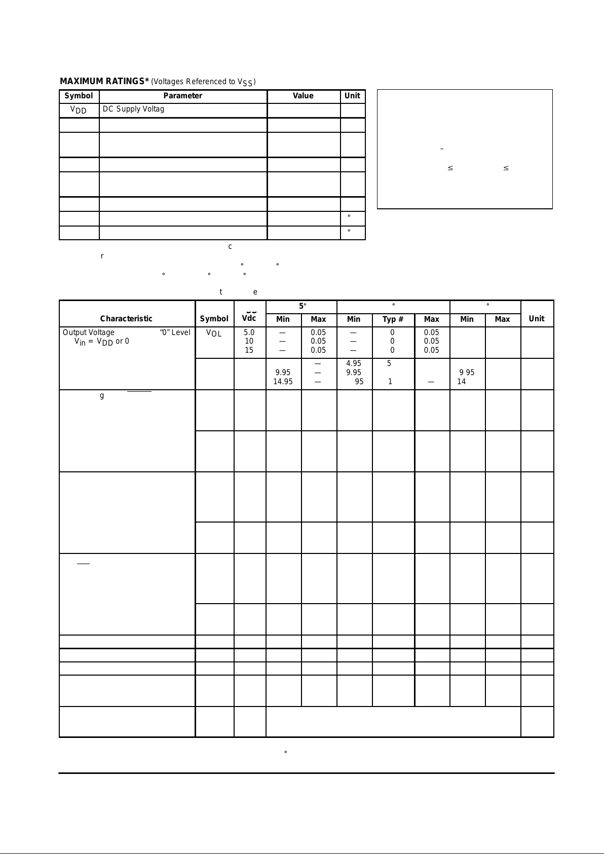
MAXIMUM RATINGS* (Voltages Referenced to V
SS
)
Symbol
Parameter Value Unit
V
DD
DC Supply Voltage – 0.5 to + 18.0 V
V
in
Input Voltage, Enable (DC or Transient) – 0.5 to VDD + 0.5 V
V
in
Input Voltage, All other Inputs
(DC or Transient)
– 0.5 to VDD + 12 V
V
out
Output Voltage (DC or Transient) – 0.5 to VDD + 0.5 V
Iin, lout Input or Output Current (DC or Transient),
per Pin
± 10 mA
P
D
Power Dissipation, per Package† 500 mW
T
stg
Storage Temperature – 65 to + 150
_
C
T
L
Lead Temperature (8–Second Soldering) 260
_
C
*Maximum Ratings are those values beyond which damage to the device may occur.
†Temperature Derating:
“P and D/DW” Packages: – 7.0 mW/C From 65_C To 125_C Ceramic
“L” Packages: – 12 mW/_C From 100_C To 125_C
ELECTRICAL CHARACTERISTICS (Voltages Referenced to V
SS
)
V
– 55_C 25_C 125_C
Characteristic
Symbol
V
DD
Vdc
Min Max Min Typ # Max Min Max
Unit
Output Voltage “0” Level
Vin = VDD or 0
V
OL
5.0
10
15
—
—
—
0.05
0.05
0.05
—
—
—
0
0
0
0.05
0.05
0.05
—
—
—
0.05
0.05
0.05
Vdc
“1” Level
Vin = 0 or V
DD
V
OH
5.0
10
15
4.95
9.95
14.95
—
—
—
4.95
9.95
14.95
5.0
10
15
—
—
—
4.95
9.95
14.95
—
—
—
Vdc
Input Voltage** — Enable “0” Level
(VO = 4.5 or 0.5 Vdc)
(VO = 9.0 or 1.0 Vdc)
(VO = 13.5 or 1.5 Vdc)
V
IL
5.0
10
15
—
—
—
0.8
1.6
2.4
—
—
—
1.1
2.2
3.4
0.8
1.6
2.4
—
—
—
0.8
1.6
2.4
Vdc
“1” Level
(VO = 0.5 or 4.5 Vdc)
(VO = 1.0 or 9.0 Vdc)
(VO = 1.5 or 13.5 Vdc)
V
IH
5.0
10
15
2.0
6.0
10
—
—
—
2.0
6.0
10
1.9
3.1
4.3
—
—
—
2.0
6.0
10
—
—
—
Vdc
Input Voltage “0” Level
Other Inputs
(VO = 4.5 or 0.5 Vdc)
(VO = 9.0 or 1.0 Vdc)
(VO = 13.5 or 1.5 Vdc)
V
IL
5.0
10
15
—
—
—
1.5
3.0
4.0
—
—
—
2.25
4.50
6.75
1.5
3.0
4.0
—
—
—
1.5
3.0
4.0
Vdc
(VO = 0.5 or 4.5 Vdc) “1” Level
(VO = 1.0 or 9.0 Vdc)
(VO = 1.5 or 13.5 Vdc)
V
IH
5.0
10
15
3.5
7.0
11
—
—
—
3.5
7.0
11
2.75
5.50
8.25
—
—
—
3.5
7.0
11
—
—
—
Vdc
Output Drive Current Source
(Full
— Sink Only)
(VOH = 4.6 Vdc)
(VOH = 9.5 Vdc)
(VOH = 13.5 Vdc)
I
OH
5.0
10
1 5
– 1.0
—
—
–
—
—
– 1.0
—
—
– 2.0
– 6.0
– 12
—
—
—
– 1.0
—
—
—
—
—
mAdc
(VOL = 0.4 Vdc) Sink
(VOL = 0.5 Vdc)
(VOL = 1.5 Vdc)
I
OL
5.0
10
15
1.6
—
—
—
—
—
1.6
—
—
3.2
6.0
12
—
—
—
1.6
—
—
—
—
—
mAdc
Input Current I
in
15 — ±0.1 — ±0.00001 ±0.1 — ±1.0 µAdc
Three–State Leakage Current I
TL
15 — ±0.1 — ±0.00001 ±0.1 — ±3.0 µAdc
Input Capacitance (Vin = 0) C
in
— — — — 5.0 7.5 — — pF
Quiescent Current
(Per Package)
I
DD
5.0
10
15
—
—
—
5.0
10
20
—
—
—
0.005
0.010
0.015
5.0
10
20
—
—
—
150
300
600
µAdc
**Total Supply Current at an
**External Load Capacitance of
**130 pF
I
T
5.0
10
IT = (2.0 µA/kHz) f + I
DD
IT = (4.0 µA/kHz) f + I
DD
IT = (6.0 µA/kHz) f + I
DD
µAdc
†Data labelled “Typ” is not to be used for design purposes but is intended as an indication of the IC’s potential performance.
**The formulas given are for the typical characteristics only at 25_C.
This device contains protection circuitry to
guard against damage due to high static
voltages or electric fields. However, precautions must be taken to avoid applications of
any voltage higher than maximum rated voltages to this high–impedance circuit. For proper
operation, Vin and V
out
should be constrained
to the range VSS v (Vin or V
out
) v VDD.
Unused inputs must always be tied to an
appropriate logic voltage level (e.g., either V
SS
or VDD). Unused outputs must be left open.
Page 3
MOTOROLA CMOS LOGIC DATA
3
MC14597B MC14598B
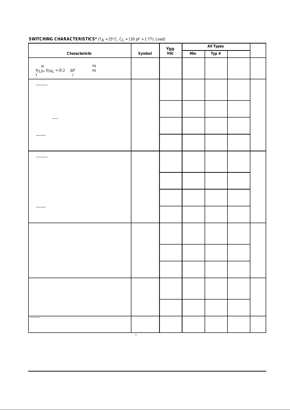
SWITCHING CHARACTERISTICS* (T
A
= 25_C, CL = 130 pF + 1 TTL Load)
V
All Types
Characteristic
Symbol
V
DD
Vdc
Min Typ # Max
Unit
Output Rise and Fall Time
t
TLH
, t
THL
= (0.5 ns/pF) CL + 35 ns
t
TLH
, t
THL
= (0.2 ns/pF) CL + 25 ns
t
TLH
, t
THL
= (0.16 ns/pF) CL + 20 ns
t
TLH
,
t
THL
5.0
10
15
—
—
—
100
50
40
200
100
80
ns
Propagation Delay Time
Enable
to Output
t
PLH
,
t
PHL
5.0
10
15
—
—
—
160
125
100
320
250
200
ns
Strobe to Output 5.0
10
15
—
—
—
200
100
80
400
200
160
Strobe to Full (MC14597B only) 5.0
10
15
—
—
—
200
100
80
400
200
160
Reset to Output 5.0
10
15
—
—
—
175
90
70
350
180
140
Pulse Width
Enable
tWH,
t
WL
5.0
10
15
320
240
160
160
120
80
—
—
—
ns
Strobe 5.0
10
15
200
100
80
100
50
40
—
—
—
Increment (MC14597B only) 5.0
10
15
200
100
80
100
50
40
—
—
—
Reset 5.0
10
15
300
160
100
150
80
50
—
—
—
Setup Time
Data
t
su
5.0
10
15
100
50
35
50
25
20
—
—
—
ns
Address (MC14598B only) 5.0
10
15
200
100
70
100
50
35
—
—
—
Increment (MC14597B only) 5.0
10
15
400
200
170
200
100
85
—
—
—
Hold Time
Data
t
h
5.0
10
15
100
50
35
50
25
20
—
—
—
ns
Address (MC14598B only) 5.0
10
15
100
50
35
50
25
20
—
—
—
Reset Removal Time t
rem
5.0
10
15
20
20
20
– 25
– 15
– 10
—
—
—
ns
*The formulas given are for the typical characteristics only at 25_C.
#Data labelled “Typ” is not to be used for design purposes but is intended as an indication of the IC’s potential performance.
Page 4

MOTOROLA CMOS LOGIC DATAMC14597B MC14598B
4
MC14597B FUNCTION DIAGRAM
ENABLE 4
RESET
2
STROBE 6
DATA 3
TO OTHER
LATCHES
TO OTHER
LATCHES
V
DD
V
DD
V
DD
V
SS
ONE LATCH
ZERO
SELECT
SEVEN
SELECT
5 FULL
1 D
0
15 D1
14 D2
13 D3
12 D4
11 D5
10 D6
9 D7
INCREMENT 7
R
CLK
3 STAGE COUNTER
AND DECODER
ADDITIONAL 7 LATCHES
R
D Q
CLK
MC14597B TIMING DIAGRAMS
NOTES:
1. High–impedance output state (another device controls bus).
2. Reset
in High state.
*1.4 V with VDD = 5.0 V
D6 (INTERNAL)
D7 (INTERNAL)
INCREMENT
DATA
STROBE
FULL
RESET
t
WL
t
WH
20 ns
90%
10%
tsut
h
t
W
10%
90%
20 ns t
PHL
t
rem
50%
t
W
D
n
FULL
ENABLE
t
TLH
t
THL
90% 90%
10%10%
t
PHL
t
WL
1
* *
NOTE: Enable in High state.
t
su
Page 5

MOTOROLA CMOS LOGIC DATA
5
MC14597B MC14598B
MC14598B FUNCTION DIAGRAM
ENABLE 4
RESET
2
STROBE 6
DATA 3
TO OTHER
LATCHES
V
DD
V
SS
EACH LATCH
ZERO
SELECT
1 D0
17 D1
16 D2
15 D3
14 D4
13 D5
12 D6
11 D7
ADDRESS
DECODER
ADDITIONAL 7 LATCHES
A0 7
A1 8
A2 10
TO OTHER
LATCHES
(M.S.B)
MC14598B TIMING DIAGRAM
*1.4 V with VDD = 5.0 V
NOTES:
1. High–impedance output state (another device controls bus).
2. Output Load as for MC14597B.
D7
RESET
A0, A1, A2
DATA
STROBE
ENABLE
90%
10%
50%
50%
t
PHL
t
PLH
1
t
THL
t
PLH
90%
10%
t
TLH
t
W
50%
20 ns
90%
10%
tsut
h
t
h
t
su
90%
10%
50%
90%
10%
20 ns t
W
20 ns
t
W
*
Page 6

MOTOROLA CMOS LOGIC DATAMC14597B MC14598B
6
TRUTH TABLE FOR MC14597B
Address
Increment Enable
Reset Counter Full
X 1 Count Up —
X 1 No Change —
X 1 0 Reset to Zero Set to One
X 0 1 No Change Set to One
If at To Zero on
X 1 1 ADDRESS 7 Falling Edge
of STROBE
X = Don’t care
LATCH TRUTH TABLE
Address Other
Strobe Reset
Latch Latches
0 1 * *
1 1 Data *
X 0 0 0
*= No change in state of latch
X = Don’t care
TEST LOAD
ALL OUTPUTS
D
n
+5.0 V
RL = 2.5 k
11.7 k
130 pF
Circuit diagrams external to or containing Motorola products are included as a means of illustration only. Complete
information sufficient for construction purposes may not be
fully illustrated. Although the information herein has been
carefully checked and is believed t o be reliable. Motorola
assumes no responsibility for inaccuracies. Information herein does not convey to the purchaser any license under the
patent rights of Motorola or others.
The information contained herein is for guidance only , with
no warranty of any type, expressed or implied. Motorola reserves the right to make any changes to the information and
the product(s) to which the information applies and to discontinue manufacture of the product(s) at any time.
Page 7

MOTOROLA CMOS LOGIC DATA
7
MC14597B MC14598B
OUTLINE DIMENSIONS
P SUFFIX
PLASTIC DIP PACKAGE
CASE 648–08
ISSUE R
NOTES:
1. DIMENSIONING AND TOLERANCING PER ANSI
Y14.5M, 1982.
2. CONTROLLING DIMENSION: INCH.
3. DIMENSION L TO CENTER OF LEADS WHEN
FORMED PARALLEL.
4. DIMENSION B DOES NOT INCLUDE MOLD FLASH.
5. ROUNDED CORNERS OPTIONAL.
–A–
B
F
C
S
H
G
D
J
L
M
16 PL
SEATING
1 8
916
K
PLANE
–T–
M
A
M
0.25 (0.010) T
DIM MIN MAX MIN MAX
MILLIMETERSINCHES
A 0.740 0.770 18.80 19.55
B 0.250 0.270 6.35 6.85
C 0.145 0.175 3.69 4.44
D 0.015 0.021 0.39 0.53
F 0.040 0.70 1.02 1.77
G 0.100 BSC 2.54 BSC
H 0.050 BSC 1.27 BSC
J 0.008 0.015 0.21 0.38
K 0.110 0.130 2.80 3.30
L 0.295 0.305 7.50 7.74
M 0 10 0 10
S 0.020 0.040 0.51 1.01
____
L SUFFIX
CERAMIC DIP PACKAGE
CASE 620–10
ISSUE V
NOTES:
1. DIMENSIONING AND TOLERANCING PER
ANSI Y14.5M, 1982.
2. CONTROLLING DIMENSION: INCH.
3. DIMENSION L TO CENTER OF LEAD WHEN
FORMED PARALLEL.
4. DIMENSION F MAY NARROW TO 0.76 (0.030)
WHERE THE LEAD ENTERS THE CERAMIC
BODY.
–A–
–B–
–T–
F
E
G
N
K
C
SEATING
PLANE
16 PLD
S
A
M
0.25 (0.010) T
16 PLJ
S
B
M
0.25 (0.010) T
M
L
DIM MIN MAX MIN MAX
MILLIMETERSINCHES
A 0.750 0.785 19.05 19.93
B 0.240 0.295 6.10 7.49
C ––– 0.200 ––– 5.08
D 0.015 0.020 0.39 0.50
E 0.050 BSC 1.27 BSC
F 0.055 0.065 1.40 1.65
G 0.100 BSC 2.54 BSC
H 0.008 0.015 0.21 0.38
K 0.125 0.170 3.18 4.31
L 0.300 BSC 7.62 BSC
M 0 15 0 15
N 0.020 0.040 0.51 1.01
_ _ _ _
16 9
1 8
Page 8

MOTOROLA CMOS LOGIC DATAMC14597B MC14598B
8
OUTLINE DIMENSIONS
D SUFFIX
PLASTIC SOIC PACKAGE
CASE 751B–05
ISSUE J
NOTES:
1. DIMENSIONING AND TOLERANCING PER ANSI
Y14.5M, 1982.
2. CONTROLLING DIMENSION: MILLIMETER.
3. DIMENSIONS A AND B DO NOT INCLUDE
MOLD PROTRUSION.
4. MAXIMUM MOLD PROTRUSION 0.15 (0.006)
PER SIDE.
5. DIMENSION D DOES NOT INCLUDE DAMBAR
PROTRUSION. ALLOWABLE DAMBAR
PROTRUSION SHALL BE 0.127 (0.005) TOTAL
IN EXCESS OF THE D DIMENSION AT
MAXIMUM MATERIAL CONDITION.
1 8
16 9
SEATING
PLANE
F
J
M
R
X 45
_
G
8 PLP
–B–
–A–
M
0.25 (0.010) B
S
–T–
D
K
C
16 PL
S
B
M
0.25 (0.010) A
S
T
DIM MIN MAX MIN MAX
INCHESMILLIMETERS
A 9.80 10.00 0.386 0.393
B 3.80 4.00 0.150 0.157
C 1.35 1.75 0.054 0.068
D 0.35 0.49 0.014 0.019
F 0.40 1.25 0.016 0.049
G 1.27 BSC 0.050 BSC
J 0.19 0.25 0.008 0.009
K 0.10 0.25 0.004 0.009
M 0 7 0 7
P 5.80 6.20 0.229 0.244
R 0.25 0.50 0.010 0.019
_ _ _ _
L SUFFIX
CERAMIC DIP PACKAGE
CASE 726–04
ISSUE G
NOTES:
1. DIMENSIONING AND TOLERANCING PER
ANSI Y14.5M, 1982.
2. CONTROLLING DIMENSION: INCH.
3. DIMENSION L TO CENTER OF LEAD WHEN
FORMED PARALLEL.
4. DIMENSION F FOR FULL LEADS. HALF
LEADS OPTIONAL AT LEAD POSITIONS 1, 9,
10, AND 18.
1
SEATING
PLANE
10
9
18
M
K
C
N
F
G
D
L
–A–
–B–
18 PL
J 18 PL
–T–
S
A
M
0.25 (0.010) T
S
B
M
0.25 (0.010) T
OPTIONAL LEAD
CONFIGURATION (1, 9, 10, 18)
DIM MIN MAX MIN MAX
MILLIMETERSINCHES
A 22.35 23.110.880 0.910
B 6.10 7.490.240 0.295
C ––– 5.08––– 0.200
D 0.38 0.530.015 0.021
G 2.54 BSC0.100 BSC
J 0.20 0.300.008 0.012
K 3.18 4.320.125 0.170
L 7.62 BSC0.300 BSC
M 0 15 0 15
N 0.51 1.020.020 0.040
_ __ _
F 1.40 1.780.055 0.070
Page 9

MOTOROLA CMOS LOGIC DATA
9
MC14597B MC14598B
P SUFFIX
PLASTIC DIP PACKAGE
CASE 707–02
ISSUE C
NOTES:
1. POSITIONAL TOLERANCE OF LEADS (D),
SHALL BE WITHIN 0.25 (0.010) AT MAXIMUM
MATERIAL CONDITION, IN RELATION TO
SEATING PLANE AND EACH OTHER.
2. DIMENSION L TO CENTER OF LEADS WHEN
FORMED PARALLEL.
3. DIMENSION B DOES NOT INCLUDE MOLD
FLASH.
1
SEATING
PLANE
10
9
18
M
A
B
K
C
N
F
G
D
H
J
L
DIM MIN MAX MIN MAX
INCHESMILLIMETERS
A 22.22 23.24 0.875 0.915
B 6.10 6.60 0.240 0.260
C 3.56 4.57 0.140 0.180
D 0.36 0.56 0.014 0.022
F 1.27 1.78 0.050 0.070
G 2.54 BSC 0.100 BSC
H 1.02 1.52 0.040 0.060
J 0.20 0.30 0.008 0.012
K 2.92 3.43 0.115 0.135
L 7.62 BSC 0.300 BSC
M 0 15 0 15
N 0.51 1.02 0.020 0.040
_ _ _ _
How to reach us:
USA/EUROPE/Locations Not Listed: Motorola Literature Distribution; JAPAN: Nippon Motorola Ltd.; Tatsumi–SPD–JLDC, 6F Seibu–Butsuryu–Center,
P.O. Box 20912; Phoenix, Arizona 85036. 1–800–441–2447 or 602–303–5454 3–14–2 Tatsumi Koto–Ku, Tokyo 135, Japan. 03–81–3521–8315
MFAX: RMFAX0@email.sps.mot.com – TOUCHTONE 602–244–6609 ASIA/PACIFIC: Motorola Semiconductors H.K. Ltd.; 8B Tai Ping Industrial Park,
INTERNET: http://Design–NET.com 51 Ting Kok Road, Tai Po, N.T., Hong Kong. 852–26629298
Motorola reserves the right to make changes without further notice to any products herein. Motorola makes no warranty , representation or guarantee regarding
the suitability of its products for any particular purpose, nor does Motorola assume any liability arising out of the application or use of any product or circuit,
and specifically disclaims any and all liability, including without limitation consequential or incidental damages. “Typical” parameters which may be provided
in Motorola data sheets and/or specifications can and do vary in different applications and actual performance may vary over time. All operating parameters,
including “Typicals” must be validated for each customer application by customer’s technical experts. Motorola does not convey any license under its patent
rights nor the rights of others. Motorola products are not designed, intended, or authorized for use as components in systems intended for surgical implant
into the body, or other applications intended to support or sustain life, or for any other application in which the failure of the Motorola product could create a
situation where personal injury or death may occur. Should Buyer purchase or use Motorola products for any such unintended or unauthorized application,
Buyer shall indemnify and hold Motorola and its officers, employees, subsidiaries, affiliates, and distributors harmless against all claims, costs, damages, and
expenses, and reasonable attorney fees arising out of, directly or indirectly, any claim of personal injury or death associated with such unintended or
unauthorized use, even if such claim alleges that Motorola was negligent regarding the design or manufacture of the part. Motorola and are registered
trademarks of Motorola, Inc. Motorola, Inc. is an Equal Opportunity/Affirmative Action Employer .
MC14597B/D
*MC14597B/D*
◊
 Loading...