

Page 1

MC145750MOTOROLA
1
Product Preview
The MC145750 is a silicon gate HCMOS device designed to encode π/4–shift
QPSK baseband signals. The device contains two 10–bit DACs for the I/Q
signal, Root–Nyquist digital filtering, and burst rising and falling e dge
processing for digital RF communication equipment. Primary applications for
this device are in products that will be used in PHS (384 kbps) and PDC
(42 kbps). It will perform up to 800 kbps data rate. It also contains PN511
random pattern generator and timing generator with PLL.
• Root–Nyquist Digital Filtering (Coefficient = 0.5)
• Burst Edge Processing Circuitry (Ramp–Up and –Down)
• Two 10–Bit DACs for I/Q Output
• Operating Voltage Range: 2.7 to 5.5 V
• PN511 Random Pattern Generator
• Conformance to RCR Standard for PHS, PDC
• Variable Data Transmission Rate up to 800 kbps (VDD = 5 V)
• Timing Generator with PLL
• QPSK Mode, Burst, and Continuous I/Q Signal Output is Performed
• Companion Device is MRFIC0001
PIN ASSIGNMENT
NC
CF
PCO
PB1
PLL
ECLK
DV
DD
DV
SS
DCLK
DS/STBY
TXD
MODE1
MODE0
TEST
NC
DRATE
QPSK
PB2NCNC
TB0
TB1
NC
TB7
BW/TB9
TNO/TB8
I
out
DAref2
DAref3
DAref
DAref1
Q
out
DAV
SS
DV
DD
NC
TB2
TB4
TB5
TB6
NC
NC
MODE2
ERST/PDN
DAV
DD
TB3
DV
SS
NC
DAb
1
48
37
36
25
24
13
12
NC = NO CONNECTION
This document contains information on a product under development. Motorola reserves the right to change or discontinue this product without notice.
Order this document
by MC145750/D
SEMICONDUCTOR TECHNICAL DATA
VFU SUFFIX
PLASTIC VQFP
CASE 932
ORDERING INFORMATION
MC145750VFU VQFP
Motorola, Inc. 1995
REV 2
10/95
Page 2

MC145750 MOTOROLA
2
BLOCK DIAGRAM
PNO/TB8
TXD
DS/STBY
DCLK
PLL
ECLK
I
out
Q
out
BW/TB9
TEST TB7:0 M2:0 QPSK DRATE DAb DAref DAref3:1
PN PATTERN
GENERATOR
TEST
CIRCUIT
π
/4–SHIFT
QPSK
ENCODER
INTERFACE
CIRCUIT
ROLL–OFF
FILTERS
10–BIT
DAC
10–BIT
DAC
DPLL
TIMING
GENERATOR
DVDDDV
SS
ERST
/PDN Cf PC0 PB1 PB2 DAV
DD
DAV
SS
I
Q
INPUT/OUTPUT TIMING RELATIONS
DS
(INPUT)
DCLK
(INPUT)
TXD
(INPUT)
BW
(OUTPUT)
I
out/Qout
(OUTPUT)
RAMP–UP
(TWO SYMBOL LENGTH)
100% OUTPUT SWING LEVEL
RAMP–DOWN
(TWO SYMBOL LENGTH)
FIRST SYMBOL
LAST SYMBOL
DON’T CARE
1 2 3 4 5 6 7 8 9
n – 1
n 1 2 3 11 14 15 16
9 10
n BIT
Page 3

MC145750MOTOROLA
3
MAXIMUM RATINGS
Parameter
Symbol
Value
Unit
DC Supply Voltage
V
DD
– 0.5 to + 7
V
DC Input Voltage
V
in
– 0.5 to VDD + 0.5
V
Power Dissipation
P
D
500
mW
Storage Temperature
T
stg
– 65 to +150
°C
RECOMMENDED OPERATING CONDITIONS
Parameter Symbol Min Typ Max Unit
DC Supply Voltage V
DD
2.7 3.3 5.5 V
DC Input Voltage V
in
0 — V
DD
V
Operating Temperature Range T
A
– 20 25 85 °C
ELECTRICAL CHARACTERISTICS (T
A
= 25°C, TXD = L, Normal Mode)
Parameters
Symbol Condition Min Typ** Max Unit
DC Supply Current
I
dd1
ERST = L — 0.25 0.5
mA
VDD = 3 V
DRATE = L I
dd2
DS = L
— 5.0 6.0
DRATE = H I
dd3
— 1.5 1.8
DRATE = L I
dd4
DS = Burst Input*
— 5.0 6.0
DRATE = H I
dd5
— 1.5 1.8
DRATE = L I
dd6
DS = Continual Input
— 8.0 10.0
DRATE = H I
dd7
— 2.0 2.6
DC Supply Current
I
dd1
ERST = L — 0.5 3.0
mA
VDD = 5 V
DRATE = L I
dd2
DS = L
— 27.0 33.0
DRATE = H I
dd3
— 17.0 19.0
DRATE = L I
dd4
DS = Burst Input*
— 30.0 33.0
DRATE = H I
dd5
— 18.0 20.0
DRATE = L I
dd6
DS = Continual Input
— 33.0 37.0
DRATE = H I
dd7
— 18.0 20.0
*625 µs burst/5 ms period (DRATE = L) at DCLK = 384 kHz.
6.6 ms burst/20 ms period (DRATE = H) at DCLK = 42 kHz.
**Typical numbers are not guaranteed.
ANALOG CHARACTERISTICS (T
A
= 25°C)
Parameters
Symbol Condition Min Typ** Max Unit
Output Swing Level
VDD = 3 V
V
out
RL = k
Ω, TXD = L
500 550 600
mV p–p
I/Q Out
VDD = 5 V
Normal Mode
520 570 620
Output Swing Imbalance ∆V
out
– 0.5 0 0.5 dB
Output DC Level
VDD = 3 V
V
out
DS = L
800 820 840
mV
I/Q Out
VDD = 5 V 780 800 820
Output Swing Imbalance ∆V
DD
— — 20
Out–of–Band Noise Level VDD = 5 V V
in
600 kHz — – 50 —
dB
900 kHz — – 55 —
DC Output Resistance R
out
I
out/Qout
— 50 100 Ω
*DAref1 = H at VDD = 3 V, DAref3 = H at VDD = 5 V
**Typical numbers are not guaranteed.
Page 4

MC145750 MOTOROLA
4
SWITCHING CHARACTERISTICS (T
A
= 25°C)
Parameters Symbol Condition Min Typ* Max Unit
Input Voltage
High–Level V
IH
VDD x 0.7 — —
V
Low–Level V
IL
— — VDD x 0.3
Output Voltage
High–Level V
OH
BW, PNO
VDD x 0.9 — —
Low–Level V
OL
— — VDD x 0.1
Data Set–Up Time t
su
TXD, DS, STBY 10 — —
ns
Data Hold Time t
h
TXD, DS, STBY 10 — —
Data Output Propagation Delay t
pd
BW, PNO — 1.5 3
µs
I/Q Output Propagation Delay T
D
I
out
, Q
out
— 4 6
Data Rate VDD = 3 V
DRATE = L — — 450
kbps
DRATE = H — — 55
VDD = 5 V
DRATE = L — — 800
DRATE = H — — 100
Clock Input Duty Cycle DCLK 45 50 55 %
VCO Oscillation Frequency
VDD = 3 V f
VCO1
— — 20
MHz
VDD = 5 V f
VCO2
— — 32
* Typical numbers are not guaranteed.
Figure 1. Timing Diagram
DS
DCLK
TXD
BW
I
out/Qout
PNO
t
su
t
su
1/fclk
t
PD
t
h
t
su
t
h
t
PD
t
su
t
h
t
D
t
PD
t
D
Page 5

MC145750MOTOROLA
5
PIN DESCRIPTIONS
POWER SUPPLY
V
SS
Digital Ground (Pins 6, 44)
These are the negative power supply input pins to the digi-
tal portion of the device and are connected to ground (0 V).
V
DD
Positive Power Supply Input (Pins 7, 43)
These are the positive power supply input pins to the digi-
tal portion of the device. Typical operating voltage range is
3.3 V at DAref3 = H, 5.0 V at DAref1 = H. Power should be
fed simultaneously with DA VDD pin in order to avoid any possible damage to the device.
DAV
DD
Positive Power Supply Input for DACs (Pin 13)
This is the positive power supply input pin to the analog
portion of the device. Typical operating voltage range is 2.7 V
to 5.5 V.
DAV
SS
Analog Ground for DACs (Pin 14)
This is the negative power supply pin to the analog portion
of the device and is connected to ground.
MODE CONTROL AND TEST
MODE0 – MODE2
Normal/Test Mode Select (Pins 1, 2, 3)
These pins must be connected to ground for normal operation. For system test, PN pattern generation mode will be
performed when MODE0 = H and MODE1, MODE2 = L.
PN511 signal is fed to the encoder instead of input data from
TXD pin. Data shift timing is the same as the normal operation mode and burst timing indicated by DS pin is still valid for
the device. The PN511 signal is monitored at the PNO pin.
TEST
Test Mode (Pin 4)
The device operates normally while this pin is held low.
When this signal is high, the device enters into factory test
mode. Only one mode is allowed to be enacted by user for
PN Mode.
DRATE
Data–Rate Select (Pin 9)
This pin can select high data rate when it is low , such as in
PHS applications.
QPSK
(D)QPSK/π/4–Shift QPSK Mode Select (Pin 10)
The device operates as a π/4–QPSK Encoder when this
pin is held high. By making this pin low, it functions as non–
shift differential QPSK Encoder. All of the functions are the
same in both modes.
PN0/TB8
PN511 Test Pattern Output/Test Bus 8 (Pin 23)
This is the output data of PN511 test–pattern in normal
mode. When the PN pattern generator outputs to this pin, it
can be output I/Q pins and data from TXD pin may be ignored. If the DS signal is L, I/Q pins stop but PN data stream
may be output.
TB0 – TB7
Test Bus (Pins 24, 26 – 32)
These pins are used in factory test and should be connected to ground for normal operation.
PLL
Int/Ext PLL Clock Select (Pin 41)
When this pin is connected to ground, the PLL is active
and timing will be generated internally. When this pin is connected to VDD, timing should be applied to the ECLK pin.
DIGITAL INTERFACE PINS
BW/TB9
Burst Window Output/Test Bus 9 (Pin 22)
This output indicates when modulated baseband I/Q signals are output from this device. This pin is used as the transmission control signal for saving power for RF.
ECLK
External Clock Input (Pin 42)
When the internal timing generator with PLL is not used in
the system, this pin must have 15.36 MHz applied as a system clock for this device. This pin is connected to ground for
normal operation.
DCLK
Data Shift Clock Input (Pin 45)
This is the shift clock input for the transmit data input and is
typically 384 kHz for the PHS (DRATE Pin = L) and 42 kHz
for the PDC (DRATE Pin = H) application. The data input occurs at the rising edge of the DCLK. For burst–type systems
such as the TDMA data transmission applications, this signal
must be synchronized with the rising/falling edge of the DS
pin (Data Slot Timing Input).
DS/STBY
Data Slot Timing/Standby Input (Pin 46)
For burst–type, this input signal indicates when transmit
data are valid for the device. Its duration must be equal with
the number of input data to the device, and its transition must
be aligned with the rising edge of the DCLK signal.
When a logic L is applied to this pin, all digital portions except the timing generator are not clocked and the device is in
a low power dissipation mode. When a logic H is applied continuously, all input data are encoded as valid data.
TXD
Transmit Data Input (Pin 47)
Data bit streams to be transmitted are input to this pin. The
data is valid only when the DS (Pin 46) is asserted (high). Its
transition should be s ynchronized with rising edge of the
DCLK (Pin 45).
Page 6

MC145750 MOTOROLA
6
ERST/PDN
External Reset/Power Down Input (Pin 48)
When a logic L is applied to this pin, it forces a complete
power down. When at start up, VDD goes high, it is recommended that a logic L, then a logic H be applied to this pin to
start up and reset all digital portions.
ANALOG INTERFACE PINS
Q
out
Filtered Quadrature–Phase Output (Pin 15)
This is the modulated quadrature–phase signal output and
the amplitude is typically 550 mV p–p at VDD = 3 V in PN test
mode. The output dc resistance is approximately 50 Ω.
I
out
Filtered In–Phase Output (Pin 20)
This is the modulated in–phase signal output and amplitude is typically 500 mV p–p at VDD = 3 V in PN test mode.
The output dc resistance is approximately 50 Ω.
DAC AND PLL SETTING
DAb
Reference Bias Setting Pin to DACs (Pin 12)
A resistor connected to ground from this pin determines
the reference current value for internal DACs. This resistor’s
value is 200 kΩ typically.
DAref
Ripple Filter Capacitor (Pin 16)
A capacitor connected to ground from this pin acts as a ripple filter for the internal DACs’ reference voltage. This capacitor’s value is 0.1µF, typically.
DAref1 – DAref3
Reference Bias Setting to DACs (Pin 17 – 19)
These pins determine the reference voltage for internal
DACs in conjunction with DAb pin. At 3 V operation, DAref1
pin should be connected to VDD. DAref2 pin should be connected to VDD at 3.3 V. DAref3 pin should be connected to
VDD at 5 V . The two other pins for the respective cases must
be left open.
PB1, PB2
PLL Bias (Pins 35, 38)
This pin determines the bias of the PLL. Its recommended
values are shown in T able 1 and it depends on operating voltage.
Cf
Loop Filter Capacitor (Pin 39)
Input from Cf pin is fed directly as the internal VCO control
signal.
PCO
Phase Comparator Output (Pin 40)
Connect an LPF as loop filter for the PLL. Refer to the application figure for recommended values.
Table 1. Function Table
Pin L H Remarks
3 MODE0 Normal Mode PN Pattern
These settings are independent of power supply.
10 QPSK Non–Shift /4–Shift
9 DRATE High Speed Low Speed To be determined setting high or low speed data rate.
17 DAref1 — VDD = 5 V
These pins should be held high depending on power supply voltage and
18 DAref2 — VDD 3.3 V
others should be left open.
19 DAref3 — VDD 3.0 V
41 PLL PLL Operation
Mode
Ext Clock Mode In case of external clock mode, TX data rate must be set to a frequency
of 1/40 when DRATE = L, and must be set to a frequency of 1/320
when DRATE = H. Max data rate is limited by power supply.
48 ERST/PDN Power Down Normal Operation Digital circuits reset condition will be released by rising edge of this
input.
Figure 2. DQPSK Baseband Signal Generation
SERIAL TO
PARALLEL
CONVERSION
DIFFERENTIAL
ENCODING
ROLL–OFF
FILTER
ROLL–OFF
FILTER
SERIAL DATA IN
Xk
Yk
Qk
Ik
TO DAC
TO DAC
Page 7

MC145750MOTOROLA
7
DEVICE DESCRIPTION
π/4–Shift QPSK Encoding
RCR standard (STD–28) specifies the basic configuration
of this modulation scheme as shown in Figure 2. First, serial
data input is converted to Xk/Yk parallel streams. Then its
value is compared with one previous symbol Ik/Qk, respectively, whether or not there is a change of polarity. If there is a
change, result is coded as 1. This two–bit πr (di–bit) is called
symbol, hence symbol rate is just half of the data input rate to
be modulated.
Phase transitions are determined as shown in Figure 3,
with respect to four di–bit values of Xk, Yk. (As is shown,
there should be at least π/4 of phase shift in each symbol timing unlike plain QPSK.) Actual in–phase outputs are fed to a
quadrature modulator circuit, and it is recommended that a
2– to 3–order LPF be used, which may be used as a level
shifter and dc offset compensation circuitry at the same time.
The reference voltage for the DACs is given by connecting
either of DAref1:3 to VDD according to the operating voltage
used. It is preferable not to have this voltage vary, since I/Q
output levels are affected.
Timing Generator
The PLL is intended in order to generate all required timing
signals for the devices. The VCO oscillating at the PN511
pattern rate is utilized when some characteristics are measured. By pulling MODE0 pin high, the device generates this
sequence. It is a useful simple measurement for the occupied power bandwidth and the out–of–band power level. The
sequence itself can also be monitored at the PNO pin.
This circuit is reset by an external reset signal while the
low–state of DS is not valid for initializing the generator.
START–UP SEQUENCE
To ensure stability and to initialize the internal ROM and
encoder, the start–up sequence should be done at power–
up. Refer to Figure 4.
Di–Bit Input
Xk Yk
Phase Shift
0 0
0 1
1 0
1 1
π/4
3π/4
– π/4
– 3π/4
Figure 3. Phase Diagram
Q
00
01
11
10
I
22.5
°
Figure 4. Start–Up Sequence
V
DD
REST
/PDN
DS
90%
> 100
µ
s
1 s
Page 8

MC145750 MOTOROLA
8
Figure 5. DRATE Equals L: 5 V Operation
NC
CF
PCO
PB1
PLL
ECLK
DV
DD
DV
SS
DCLK
DS/STBY
TXD
M1M0TEST
NC
DRATE
QPSK
PB2
NC
NC
TB0
TB1
NC
TB7
BW/TB9
PNO/TB8
I
out
DAref2
DAref3
DAref
DAref1
Q
out
DAV
SS
DV
DD
NC
TB2
TB4
TB5
TB6
NC
NC
M2
ERST/PDN
DAV
DD
TB3
DV
SS
NC
DAb
3635343332313029282726
25
CP
2
3
4
5
678
9
101112
24
23
22
21
20
19
18
17
16
15
14
13
37
38
39
40
41
42
43
44
45
46
47
48
47 k
I OUTPUT
Q OUTPUT
5 V
0.1
µ
10
µ
10 k
384 kHz
BURST TIMING OUTPUT
BURST TIMING INPUT
TX DATA INPUT
EXTERNAL RESET INPUT
1
µ
0.1
µ
10
µ
33 k
33 k
220 k
100 p
0.1
µ
1000 p
2.2 k
0.1
µ
0.1 µ10
µ
MC145750
Figure 6. DRATE Equals H: 3 V Operation
NC
CF
PCO
PB1
PLL
ECLK
DV
DD
DV
SS
DCLK
DS/STBY
TXD
M1M0TEST
NC
DRATE
QPSK
PB2
NC
NC
TB0
TB1
NC
TB7
BW/TB9
PNO/TB8
I
out
DAref2
DAref3
DAref
DAref1
Q
out
DAV
SS
DV
DD
NC
TB2
TB4
TB5
TB6
NC
NCM2
ERST/PDN
DAV
DD
TB3
DV
SS
NC
DAb
3635343332
31302928272625
CP
2
3
4
5
6
7
8
9
101112
24
23
22
21
20
19
18
17
16
15
14
13
37
38
39
40
41
42
43
44
45
46
47
48
47 k
I OUTPUT
Q OUTPUT
3 V
0.1
µ
10
µ
220 k
384 kHz
BURST TIMING OUTPUT
BURST TIMING INPUT
TX DATA INPUT
EXTERNAL RESET INPUT
1
µ
0.1
µ
10
µ
33 k
33 k
47 k
100 p
0.1
µ
1000 p
2.2 k
0.1
µ
0.1 µ10
µ
MC145750
Page 9

MC145750MOTOROLA
9
Figure 7. I/Q Output Interface Circuit 1
MC145750
I/Q OUTPUT
LEVEL SHIFT
BALANCE CONTROL
TO MRFIC0001
MODULATOR
R
R
R
R
+
–
+
–
Figure 8. I/Q Output Interface Circuit 2
MC145750
I/Q OUTPUT
LEVEL SHIFT
BALANCE CONTROL
TO MRFIC0001
MODULATOR
R
R
R
R
+
–
+
–
Figure 9. Modulation Accuracy Measurement Schematic
Measurement Equipment: Advantest Spectrum Analyzer R3365
Advantest Modulation Accuracy Analyzer R3541A
Rohde & Schwarz Modulation Unit SMHU–58
Conditions: Internal PLL mode, 384 kbps (PHS), TA = 25°C
220 µF
220 µF
100 k
100 k
+ 5 V
– 5 V
+ 5 V
– 5 V
I
in
Q
in
MODULATION UNIT
SMHU–58
(Zin = 50
Ω
)
IF
(240 MHz)
SPECTRUM
ANALYZER
R3365
MODULATION
ACCURACY
ANALYZER
R3541A
MC145750
I
out
+
–
Q
out
+
–
Motorola cannot recommend one supplier over another and in no way suggests
that this is a complete listing of measurement equipment suppliers.
Page 10
MC145750 MOTOROLA
10
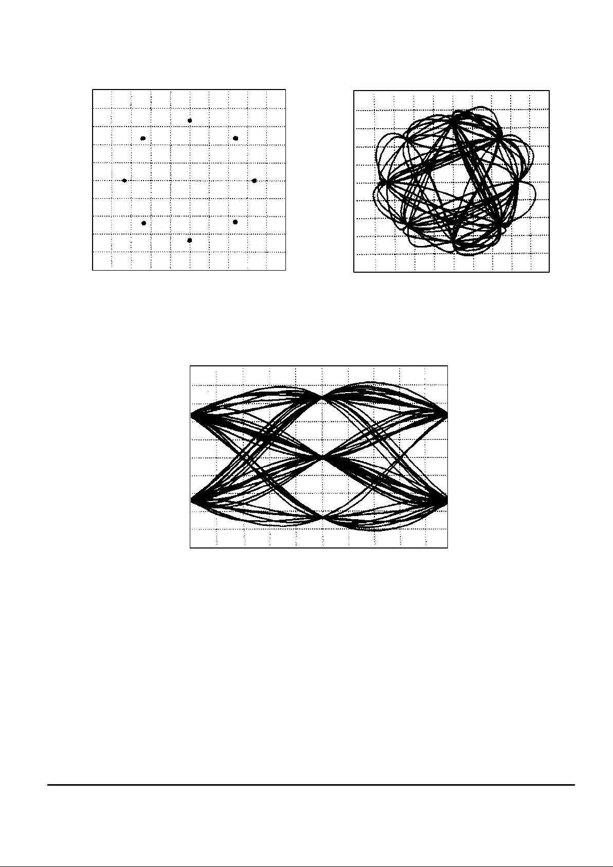
Figure 10. I–Q Pattern
1.5
1.2
0.9
0.6
0.3
0.0
– 0.3
– 0.6
– 0.9
– 1.2
– 1.5 – 1.2 – 0.9 – 0.6 – 0.3 0.0 0.3 0.6 0.9 1.2 1.5
ERR VEC : 0.982% rms
Q (t)
I (t)
Figure 11. I–Q Pattern
1.5
1.2
0.9
0.6
0.3
0.0
– 0.3
– 0.6
– 0.9
– 1.2
– 1.5 – 1.2 – 0.9 – 0.6 – 0.3 0.0 0.3 0.6 0.9 1.2 1.5
ERR VEC : 0.982% rms
I (t)
– 1.5
Q (t)
Figure 12. Q–Eye Pattern
1.5
1.2
0.9
0.6
0.3
0.0
– 0.3
– 0.6
– 0.9
– 1.2
0.0 0.2 0.4 0.6 0.8 1.0 1.2 1.4 1.6 1.8 2.0
ERR VEC : 0.982% rms
TIME
– 1.5
Q (t)
Page 11

MC145750MOTOROLA
11
PACKAGE DIMENSIONS
VFU SUFFIX
PLASTIC VQFP
CASE 932–02
DIMAMIN MAX MIN MAX
INCHES
7.000 BSC 0.276 BSC
MILLIMETERS
A1 3.500 BSC 0.138 BSC
B 7.000 BSC 0.276 BSC
B1 3.500 BSC 0.138 BSC
C 1.400 1.600 0.055 0.063
D 0.170 0.270 0.007 0.011
E 1.350 1.450 0.053 0.057
F 0.170 0.230 0.007 0.009
G 0.500 BASIC 0.020 BASIC
H 0.050 0.150 0.002 0.006
J 0.090 0.200 0.004 0.008
K 0.500 0.700 0.020 0.028
M 12 REF 12 REF
N 0.090 0.160 0.004 0.006
P 0.250 BASIC 0.010 BASIC
Q 1 5 1 5
R 0.150 0.250 0.006 0.010
S 9.000 BSC 0.354 BSC
S1 4.500 BSC 0.177 BSC
V 9.000 BSC 0.354 BSC
V1 4.500 BSC 0.177 BSC
W 0.200 REF 0.008 REF
X 1.000 REF 0.039 REF
NOTES:
1. DIMENSIONING AND TOLERANCING PER ANSI
Y14.5M, 1982.
2. CONTROLLING DIMENSION: MILLIMETER.
3. DATUM PLANE –AB– IS LOCATED AT BOTTOM OF
LEAD AND IS COINCIDENT WITH THE LEAD
WHERE THE LEAD EXITS THE PLASTIC BODY AT
THE BOTTOM OF THE PARTING LINE.
4. DATUMS –T–, –U–, AND –Z– TO BE DETERMINED
AT DATUM PLANE –AB–.
5. DIMENSIONS S AND V TO BE DETERMINED AT
SEATING PLANE –AC–.
6. DIMENSIONS A AND B DO NOT INCLUDE MOLD
PROTRUSION. ALLOWABLE PROTRUSION IS
0.250 (0.010) PER SIDE. DIMENSIONS A AND B DO
INCLUDE MOLD MISMATCH AND ARE
DETERMINED AT DATUM PLANE –AB–.
7. DIMENSION D DOES NOT INCLUDE DAMBAR
PROTRUSION. DAMBAR PROTRUSION SHALL
NOT CAUSE THE D DIMENSION TO EXCEED
0.350 (0.014).
8. MINIMUM SOLDER PLATE THICKNESS SHALL BE
0.0076 (0.0003).
9. EXACT SHAPE OF EACH CORNER IS OPTIONAL.
_ _
_ _ _ _
ÉÉÉ
ÉÉÉ
ÉÉÉ
A
A1
–T–
Z0.200 (0.008) AB T–U
–U–
4X
Z0.200 (0.008) AC T–U
4X
B
B1
1
12
13
24
25
36
37
48
–Z–
S1
S
V
V1
P
AE AE
–T–, –U–, –Z–
DETAIL Y
DETAIL Y
BASE METAL
N
J
F
D
S
T–U
M
0.080 (0.003) Z
S
AC
SECTION AE–AE
–AB–
–AC–
AD
G
0.080 (0.003) AC
M
_
TOP & BOTTOM
Q
_
W
K
X
E
C
H
0.250 (0.010)
GAUGE PLANE
R
9
DETAIL AD
Page 12

MC145750 MOTOROLA
12
Motorola reserves the right to make changes without further notice to any products herein. Motorola makes no warranty, representation or guarantee regarding
the suitability of its products for any particular purpose, nor does Motorola assume any liability arising out of the application or use of any product or circuit,
and specifically disclaims any and all liability, including without limitation consequential or incidental damages. “T ypical” parameters can and do vary in different
applications. All operating parameters, including “T ypicals” must be validated for each customer application by customer’s technical experts. Motorola does
not convey any license under its patent rights nor the rights of others. Motorola products are not designed, intended, or authorized for use as components in
systems intended for surgical implant into the body, or other applications intended to support or sustain life, or for any other application in which the failure of
the Motorola product could create a situation where personal injury or death may occur. Should Buyer purchase or use Motorola products for any such
unintended or unauthorized application, Buyer shall indemnify and hold Motorola and its officers, employees, subsidiaries, affiliates, and distributors harmless
against all claims, costs, damages, and expenses, and reasonable attorney fees arising out of, directly or indirectly, any claim of personal injury or death
associated with such unintended or unauthorized use, even if such claim alleges that Motorola was negligent regarding the design or manufacture of the part.
Motorola and are registered trademarks of Motorola, Inc. Motorola, Inc. is an Equal Opportunity/Affirmative Action Employer.
How to reach us:
USA/EUROPE: Motorola Literature Distribution; JAPAN: Nippon Motorola Ltd.; Tatsumi–SPD–JLDC, Toshikatsu Otsuki,
P.O. Box 20912; Phoenix, Arizona 85036. 1–800–441–2447 6F Seibu–Butsuryu–Center, 3–14–2 Tatsumi Koto–Ku, Tokyo 135, Japan. 03–3521–8315
MFAX: RMFAX0@email.sps.mot.com – TOUCHTONE (602) 244–6609 HONG KONG: Motorola Semiconductors H.K. Ltd.; 8B Tai Ping Industrial Park,
INTERNET: http://Design–NET.com 51 Ting Kok Road, Tai Po, N.T., Hong Kong. 852–26629298
MC145750/D
*MC145750/D*
◊
 Loading...