

Page 1

MC145745MOTOROLA
1
Product Preview
The MC145745 is a selectable modem chip compatible with ITU V.21
(300 baud full duplex asynchronous) and V.23 mode 2 (1200 baud half duplex
asynchronous). The built–in differential line driver has the capability of driving
0 dBm into a 600 Ω load with a 5 V single power supply. This device also
includes a DTMF generator, DTMF receiver, call–progress tone detector,
answer tone generator, and a receive timing control circuit.
Besides having a clock generator with a crystal oscillator connected to it, the
device has a divider circuit to which input of a double frequency clock is possible
from external sources, such as from a microcontroller unit (MCU). The serial
control port (SCP) permits the MCU to access internal registers for exercising
the built–in features.
A low consumption device, the MC145745 integrates various functions in a
small package. This modem IC is best suited for telemeter and other
applications of this type.
• Conforms to ITU V.21 and V.23 Recommendations
• DTMF Generator and Receiver for all 16 Standard Digits
• Capable of Driving 0 dBm into a 600 Ω Load (VCC = 5 V)
• Automatic Gain Control (AGC) Amplifier for the DTMF Receiver
• Call–Progress Tone Detector
• Four–Wire Serial Data Interface (SCP)
• Programmable Transmission and Carrier Detection Levels
• FSK/DTMF Analog Loopback Self–Test Function
• Crystal Oscillator (3.579545 MHz) and Half Divider Circuit (7.159090 MHz)
for External Inputs
• Operates in the Voltage Range of 3.3 – 5.5 V
• Power Down Mode (ICC < 1 µA)
This document contains information on a product under development. Motorola reserves the right to change or discontinue this product without notice.
Order this document
by MC145745/D
SEMICONDUCTOR TECHNICAL DATA
PIN ASSIGNMENT
FW SUFFIX
SOIC
CASE 751M
ORDERING INFORMATION
MC145745FW SOIC
28
1
5
4
3
2
1
10
9
8
7
6
11
12
13
14
20
21
22
23
24
25
26
19
27
28
18
17
16
15
GND
V
ref
CDA
TLA
TEST 1
RxD
TxD
CD
CLKO
X1
X2
ECLK
PB0
GND
V
CC
RxA
TxA1
TxA2
TEST 2
SCPEN
SCPCLK
SCP Rx
SCP Tx
RESET
PB3
PB2
PB1
V
CC
Motorola, Inc. 1996
REV 0
7/96
Page 2
MC145745 MOTOROLA
2
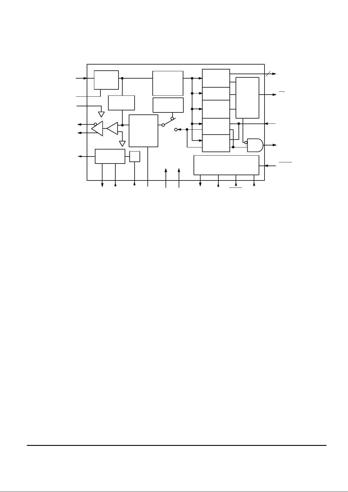
BLOCK DIAGRAM
RxA
CDA
V
ref
TxA2
TxA1
CLKO
PB0 – PB3
CD
TxD
RxD
RESET
X1 X2 ECLK TLA VCCGND SCP Tx SCP Rx SCPEN SCPCLK
Rx AMP
AND AGC
CONTROL
LOOPBACK
PATH
SMOOTHING
FILTER
AND
Tx GAIN
CONTROL
TONE
GENERATOR
ANTI–ALIAS
AND
LOW–PASS
FILTER
CLOCK
GENERATOR
1/2
DTMF
RECEIVER
CPT
DETECTOR
FSK
CARRIER
DETECTOR
FSK V.21
MODEM
FSK V.23
MODEM
4
–
+
TIMING
CONTROL
CIRCUIT
Page 3

MC145745MOTOROLA
3
PIN DESCRIPTIONS
Pin
Location
Symbol Type Description
1, 14 GND — Ground — These are the ground pins of the digital and the analog circuits. The 0 V potential of the
device is determined by the input voltage at these pins.
2 V
ref
— Reference Analog Ground — This pin provides the analog ground voltage VCC/2, which is regulated
internally . This pin should be decoupled to GND with 0.1 µF and 100 µF capacitors.
3 CDA — Carrier Detect Level Adjustment — The detection level for FSK/call–progress tone is determined
according to the voltage at this pin. When VCC = 5 V and the carrier detection level bit (BR3:b1) of the
SCP register is 0, or when VCC = 3.6 V and (BR3:b1) is 1, the CDA voltage is set to 1.25 V by the
internal divider.
This voltage sets the detection levels at ON to OFF: – 44 dBm (typ) and OFF to ON: – 47 dBm (typ).
This high impedance pin should be decoupled to GND with a 0.1 µF capacitor.
The carrier detection level is proportional to the terminal voltage at this pin.
An external voltage may be applied to this pin to adjust the carrier detect threshold. The following
equations may be used to find the CDA voltage requirements for a given threshold voltage.
V
CDA
= 256 x V
on
V
CDA
= 362 x V
off
4 TLA — Transmit Level Adjustment — This pin is used to adjust the transmit carrier level which is determined
by the resistor (RTLA) connected between this pin and GND. The maximum level is obtained when
this pin is shorted to GND (RTLA = 0).
5, 24 TEST 1,
TEST 2
I/O Test Pins 1 and 2 — These test pins are for manufacturer’s use only. These pins should be left open in
normal operation.
6 RxD O Receive Data Output — This pin is the receive data output. When the device is in the FSK mode, logic
high on this pin indicates that the mark carrier frequency has been received from RxA, and the logic
low indicates that the space carrier frequency has been received.
7 TxD I Transmit Data Input — This pin is the transmit data input. When the device is in the FSK mode, logic
high on this pin generates the mark frequency at TxA1 and TxA2 output, and logic low generates the
space frequency.
8 CD O Carrier Detect Output — This pin outputs at low level if a valid FSK, DTMF, or CPTD signal is
received. If the pin is at high level, the receive data output pin (RxD) is internally clamped at high level
to avoid erroneous output of received data caused by line noise.
9 CLKO O Clock Output — This pin provides a buffered 3.58 MHz clock output that can drive one CMOS device
such as the MC74HC04.
10 X1 O Crystal Oscillator Circuit Output — A 3.579545 MHz ± 0.1% crystal oscillator is tied to this pin with the
other end connected to X2.
11 X2 I Crystal Oscillator Circuit Input — A 3.579545 MHz ± 0.1% crystal oscillator is tied to this pin with the
other end connected to X1. X2 may be driven directly from an appropriate external clock source.
12 ECLK I External Clock Input — ECLK is the input of double frequency, 7.159090 MHz ± 0.1%, of the reference
clock. This pin must be connected to GND when not in use.
13 PB0 O DTMF Receive Data Parallel Output 0 (LSB) — Pins 13, 16, 17, and 18 are the DTMF receive data
parallel output occurring together with the CD
(Pin 8) data valid output. The outputs of these pins are
valid as long as the CD
pin is low. In power down modes 1 and 2, the DTMF receiver is disabled and
these pins are in high impedance.
15, 28 V
CC
— Positive Power Supply — These are the power supply pins for the digital and the analog circuits.
These pins should be decoupled to GND with 0.1 µF and 100 µF capacitors.
—
16, 17, 18
PB1, PB2
,
O
DTMF Receive Data Parallel Outputs 1, 2, and 3 (MSB)
—
These pins are the DTMF receiver data
PB3
parallel outputs. See pin 13 for more details.
19 RESET I Reset — A high to low trigger pulse applied to this pin sets all the registers in the default state. It
should remain at high during normal operations.
20 SCP Tx O SCP Output Transmit — Refer to Serial Control Port (SCP Interface) for additional information.
21 SCP Rx I SCP Receive Input — Refer to Serial Control Port (SCP Interface) for additional information.
22 SCPCLK I SCP Clock — Refer to Serial Control Port (SCP Interface) for additional information.
23 SCPEN I SCP Enable — Refer to Serial Control Port (SCP Interface) for additional information.
Page 4
MC145745 MOTOROLA
4
PIN DESCRIPTIONS (continued)
Pin
Location
DescriptionTypeSymbol
25 TxA2 O Transmit Buffer Output 2 (Inverting) — This pin is the inverting output of the line driver. When VCC =
5 V , + 7 dBm (typ), differential output voltage (V
TxA1
– V
TxA2
), can be obtained with a load of 1.2 kΩ
between pins TxA1 and TxA2. In typical applications, the output level on the telephone line will be half
of the differential output (refer to Application Circuit).
26 TxA1 O Transmit Buffer Output 1 (Non–Inverting) — This pin is the non–inverting output of the line driver.
Refer to TxA2.
27 RxA I Receive Signal Input — This pin is the analog signal input which has 500 kΩ input resistance (typ).
ABSOLUTE MAXIMUM RATINGS
Rating Symbol Value Unit
DC Supply Voltage V
CC
– 0.5 to + 7.0 V
DC Input Voltage V
in
– 0.5 to VCC + 0.5 V
DC Output Voltage V
out
– 0.5 to VCC + 0.5 V
DC Input Current I
in
± 20 mA
DC Output Current I
out
± 25 mA
Power Dissipation P
D
500 mW
Storage Temperature Range T
stg
– 65 to + 150 °C
RECOMMENDED OPERATIONAL CONDITIONS
Parameter Symbol Min Typ Max Unit
DC Supply Voltage V
CC
3.3 5.0 5.5 V
DC Input Voltage V
in
0 — V
CC
V
DC Output Voltage V
out
0 — V
CC
V
Crystal Oscillation Frequency f
osc
— 3.579545 — MHz
External Input Frequency (ECLK) — 7.15909 —
Operating Temperature Range T
A
– 30 25 + 85 °C
DC ELECTRICAL CHARACTERISTICS (V
CC
= + 3.3 to + 5.5 V, TA = – 30 to + 85°C)
Characteristic
Symbol Conditions Min Typ Max Unit
Input Voltage
(TxD, ECLK, RESET
,
High Level V
IH
0.7 x V
CC
— —
V
(
SCP Rx, SCPCLK,
SCPEN
)
Low Level V
IL
— — 1.1
Output Voltage
High Level V
OH
Vin = VIH or VIL, I
out
= 20 µA VCC – 0.1 VCC – 0.01 —
(RxD, CD, CLKO,
PB0–3, SCP Tx)
Low Level V
OL
Vin = VIH or V
IL
I
out
= 20 µA
I
out
= 2 mA
—
—
0.01
—
0.1
0.4
Input Leakage Current
(TxD, ECLK, RESET
, SCP Rx,
SCPCLK, SCPEN
)
I
in
Vin = VCC or GND — ± 1.0 ± 10.0 µA
Quiescent Supply
Current
VCC = 5 V I
CC
FSK Mode, RTLA = 0
TxA1 and TxA2 open
— 7 —
mA
DTMF Receive Mode, no input — 9 —
VCC = 3.6 V I
CC
FSK Mode, RTLA = 0
TxA1 and TxA2 open
— 6 —
DTMF Receive Mode, no input — 8 —
Power–Down Supply Current I
CC
Power–Down Mode 1 — — 500 µA
Power–Down Mode 2 — — 1.0 µA
This device contains circuitry to protect the
inputs against damage due to high static
voltages or electric fields. However, it is advised
that normal precautions be taken to avoid applications of any voltage higher than maximum
rated voltages to this high impedance circuit. For
proper operation, it is recommended that Vin and
V
out
be constrained to the range GND v (Vin or
V
out
) v VCC.
Reliability of operation is enhanced if unused
logic inputs are tied to an appropriate logic voltage level (e.g., either GND or VCC).
Page 5
MC145745MOTOROLA
5
AC ELECTRICAL CHARACTERISTICS
(VCC = + 3.6 V ± 0.3 V, TA = – 30 to + 85_C)
TRANSMIT CARRIER CHARACTERISTICS
Characteristic Symbol Conditions Min Typ Max Unit
V .21 Carrier Frequency
Mark “1” f
1M
Oscillation Frequency:
974 980 986
Hz
Originate Mode
Space “0” f
1S
3.579545 MHz (X2)
or 7.159090 MHz (ECLK)
1174 1180 1186
V .21 Carrier Frequency
Mark “1” f
2M
or 7.159090 MHz (ECLK)
1644 1650 1656
Answer Mode
Space “0” f
2S
1844 1850 1856
V .23 Carrier Frequency
Mark “1” f
1M
1294 1300 1306
Space “0” f
1S
2094 2100 2106
Transmit Carrier Level V
O
Transmit Attenuator = 0 dB
— 4 — dBm
Secondary Harmonic Level V
2h
RTLA = 0, RL = 1.2 kΩ
V
TxA1
– V
TxA2
— – 40 — dB
Out–of–Band Level V
OE
V
TxA1
V
TxA2
Refer to Figure 1 dBm
TRANSMIT ATTENUATOR CHARACTERISTICS
Characteristic Symbol Conditions Min Typ Max Unit
Attenuation Range 0 — 15 dB
Attenuator Accuracy 1 – 5 dB
6 – 9 dB
10 – 15 dB
– 0.5
– 1
– 1.7
—
—
—
0.5
1
1
dB
RECEIVER CHARACTERISTICS (Includes Hybrid, Demodulator , and Carrier Detector)
Characteristic Symbol Conditions Min Typ Max Unit
Input Resistance R
IRX
50 500 — kΩ
Receive Carrier Amplitude V
IRX
– 48 — – 12 dBm
Carrier Detection
OFF to ON V
CDON
CDA = 1.25 V
— – 44 —
dBm
Threshold
ON to OFF V
CDOFF
fin = 1.0 kHz
BR3 (b1) = 1
— – 47 —
Hysteresis (V
CDON
– V
CDOFF
) H
YS
BR3 (b1) = 1
2 — — dB
Carrier Detection Timing OFF to ON T
CDON
CD1 = 0, CD0 = 0, CD Pin — 450 — ms
CD1 = 0, CD0 = 1, CD Pin — 15 —
CD1 = 1, CD0 = 0, CD Pin — 15 —
CD1 = 1, CD0 = 1, CD Pin — 75 —
ON to OFF T
CDOFF
CD1 = 0, CD0 = 0, CD Pin — 30 —
CD1 = 0, CD0 = 1, CD Pin — 30 —
CD1 = 1, CD0 = 0, CD Pin — 15 —
CD1 = 1, CD0 = 1, CD Pin — 10 —
CPTD CHARACTERISTICS
Characteristic Symbol Conditions Min Typ Max Unit
BPF Center Frequency f
c
— 400 — Hz
BPF Pass–Band Lower Cut–Off
Frequency
f
i
– 3 dB — 330 — Hz
BPF Pass–Band Upper Cut–Off
Frequency
f
h
– 3 dB — 470 — Hz
CPT Detection Level
VTD ON V
TDON
CDA = 1.25 V
— – 44 —
dBm
VTD OFF V
TDOFF
fin = 400 Hz
BR3 (b1) = 1
— – 47 —
CPT Detection Timing
TTD ON T
TDON
BR3 (b1) = 1
— 10 —
ms
TTD OFF T
TDOFF
— 25 —
Page 6

MC145745 MOTOROLA
6
DTMF TRANSMIT CHARACTERISTICS
Characteristic Symbol Conditions Min Typ Max Unit
Tone Output Level
Low Group V
fl
Transmit Attenuator = 0 dB
— 0 — dBm
High Group V
fh
RTLA = 0 Ω
f
= 3.579545 MHz
— 1 — dBm
High Group Pre–Emphasis P
E
f
osc
= 3.
579545 MHz
Single Tone Mode
0 — 3 dB
DTMF Distortion DIST
R
L
= 1.2 kΩ
V
TxA1
– V
TxA2
— 5 — %
DTMF Frequency Deviation ∆f
V
V
TxA1
V
TxA2
– 1 — 1 %
Out–of–Band Level V
OE
Refer to Figure 1 dB
Setup Time t
osc
— 4 — ms
DTMF RECEIVER CHARACTERISTICS
Characteristic Symbol Conditions Min Typ Max Unit
Input Resistance 50 500 — kΩ
Detection Signal Level (Each Tone) BR3 = (0, 0, 1, 0) – 48 — 0 dBm
Twist (High/Low Group) – 10 — 10 dB
Frequency Detection Band Width
(Figure 3)
1.5% + 2 Hz
– 1.5% – 2Hz
—
—
—
—
Frequency Non–Detection Band Width
(Figure 3)
— — ± 3.5%
DTMF Detection Timing
OFF to ON
TDV
ON
CD1 = 0 , CD0 = 0 — 30 —
ms
(Figure 2) Delay
CD1 = 0 , CD0 = 1 — 35 —
CD1 = 1 , CD0 = 0 — 45 —
ON to OFF
TDV
OFF
CD1 = 0 , CD0 = 0 — 25 —
Delay
CD1 = 0 , CD0 = 1 — 35 —
CD1 = 1 , CD0 = 0 — 25 —
DEMODULATOR CHARACTERISTICS
Characteristic Symbol Conditions Min Typ Max Unit
V.21 Bit Bias Receive Level = – 24 dBm
S/N = 4 dB
— 5 — %
V .23 Bit Bias Receive Level = – 24 dBm
S/N = 14 dB
— 10 — %
V .21 Bit Error Rate Receive Level = – 24 dBm
S/N = 4 dB
511–Bit Pattern
— 0.00001 —
V .23 Bit Error Rate Receive Level = – 24 dBm
S/N = 14 dB
511–Bit Pattern
— 0.00001 —
Page 7

MC145745MOTOROLA
7
Figure 1. Out–of–Band Level
– 55
– 15 dB/OCT.
f (Hz)
256 k16 k4 k3.4 k0
0
– 25
TRANSMIT CARRIER LEVEL (dBr)
Figure 2. FSK, DTMF, and CPT Carrier Detection Timing
V
on
V
off
RxA
CD
t
off
t
on
Figure 3. DTMF Frequency Detection Bandwidth
NO–DETECT
DETECT MINIMUM
WIDTH
NO–DETECT
– 3.5%
– 1.5% – 2 Hz + 1.5% + 2 Hz
+ 3.5%
f
o
Page 8

MC145745 MOTOROLA
8
SCP TIMING CHARACTERISTICS
Ref.
No.
Characteristic Min Max Unit
1 SCPEN Active Before Rising Edge of SCPCLK 50 — ns
2 SCPCLK Rising Edge Before SCPEN Active 50 — ns
3 SCP Rx Setup Time Before SCPCLK Rising Edge 35 — ns
4 SCP Rx Hold Time After SCPCLK Rising Edge 20 — ns
5 SCPCLK Period 250 — ns
6 SCPCLK Pulse Width (Low) 50 — ns
7 SCPCLK Pulse Width (High) 50 — ns
8 SCP Tx Active Delay Time 0 50 ns
9 SCPCLK Falling Edge to SCP Tx High Impedance — 30 ns
10 SCPEN Inactive Before SCPCLK Rising Edge 50 — ns
11 SCPCLK Rising Edge Before SCPEN Inactive 50 — ns
12 SCPCLK Falling Edge to SCP Tx Valid Data 0 50 ns
Figure 4. Serial Control Port Timing
SCP Rx
R/W A2 A1 A0 D3 D2 D1
D0
123456789
21
3
4
5
7
6
11
D3 D2 D1
D0
SCP Tx
9
12
8
10
SCPEN
SCPCLK
Page 9

MC145745MOTOROLA
9
DEVICE DESCRIPTION
The MC145745 is a selectable modem chip compatible
with V.21 (300 baud full duplex asynchronous) and V.23
mode 2 (1200 baud half duplex asynchronous). This device
includes a DTMF generator, DTMF receiver, call–progress
tone detector, answer tone generator, and a receive timing
control circuit. The built–in differential line driver has the
capability of driving 0 dBm into a 600 Ω load with a 5.0 V
single power supply. The MC145745 also includes a serial
control port (SCP) that permits an MCU to exercise the built–
in features.
The MC145745 provides an SCP interface to access an internal byte register which controls the device operations;
such as function mode, carrier detect timing, transmit/receive
gain, and transmit tones.
The transmit and receive amplifiers’ gain is programmable
by SCP register setting (BR4). The TLA pin is also available
to adjust the transmit level that is determined by the resistor
(RTLA) value connected between the pin and GND. The
DTMF receiver amplifier includes a built–in AGC amplifier
which automatically adjusts the input amplifier gain corresponding to the amplitude of the DTMF tone input signal. The
AGC dynamic range can be selected in four options. The
highest received sensitivity obtained is approximately
– 50 dBm when the dynamic range of the AGC amplifier is
maximized.
The tone generator, which can generate 16 DTMF tones,
is used at the terminal for transmission of the call and control
tones. In addition, a single tone can be generated for tests
and other uses.
Power down is amenable to software control by setting the
byte register BR2. While the device is in the power down
state, SCP still operates independently. There are two power
down options available: power down 1 (the system clock
operates alone) and power down 2 (the system clock stops).
The clock generator constitutes an oscillation circuit with a
3.58 MHz crystal connected between the X1 and X2 pins.
This device also has a 7.15909 MHz external clock input
(ECLK), which has a clock divider circuit for providing a
3.58 MHz clock to the internal circuits. If the ECLK pin is
used, the X2 pin should be held low. If the oscillation circuit
(X1 and X2) is used, the ECLK pin should be held low. This
device also has a clock buffer output (CLKO), which can be
used for providing a 3.58 MHz clock to the external device.
Table 1 shows the clock input and output relations in the different modes.
Table 1. Clock Selection Truth Table
Input Output
Function Mode
ECLK
(Pin 12)
X2
(Pin 11)
CLKO
(Pin 9)
0 fxtal fxtal
Power Down 1
fext 0 fext/2
0 X 0
Power Down 2
fext 0 0
0 fxtal fxtal
Other Mode
fext 0 fext/2
SERIAL CONTROL PORT (SCP INTERFACE)
The MC145745 is equipped with an SCP. The SCP is a
full–duplex four–wire interface with control and status information passed to and from the internal register. The SCP
is compatible with the Serial Peripheral Interface (SPI) of
single chip MCUs used in other standard Motorola devices.
The SCP consists of SCP Tx, SCP Rx, SCPCLK, and
SCPEN
for transmitting control data, status data, and DTMF
receive data between the MCU and the MC145745. The
SCPCLK determines the transmission and reception data
rates, and the SCPEN
governs when the data transaction is
to take place.
The operation/configuration of the MC145745 is programmed by setting the state of the internal register bit. The
control, status, and data information resides in 4–bit wide
registers which are accessed via the 8–bit SCP bus transaction.
The first four bits of the 8–bit bus transaction are the read/
write direction and the register address. The next four bits
are the data written to or read from the internal registers.
The SCP interface is independent of the 3.58 MHz master
clock. It runs by using SCPCLK as the synchronizing signal.
SCP TRANSACTION
The SCP interface includes both read and write capabilities, which together comprise the SCP transaction. These
SCP transaction functionalities are described below.
SCP Read
The SCP read action transaction is shown in Figure 5. During the SCP read action, the SCPEN
pin must be in the low
position. After SCPEN
high goes low, then at the first four
SCPCLK rising edges, Read/Write (R/W) bit and three address bits (A0 – A2) are shifted into the intermediate buffer
register. If the read action is to be performed, the R/W
bit
must be at 1. And then, at the following four SCPCLK falling
edges, the 4–bit chosen register data is shifted out on
SCP Tx. SCPEN
must be restored to high after this transaction, before another falling edge of SCPCLK is encountered. While SCP Tx is in output mode, SCP Rx is
disregarded. Also, whenever SCP Tx is not transmitting data,
a high impedance condition is maintained.
SCP Write
The SCP write action transaction is shown in Figure 6.
During the SCP write action, the SCPEN
pin must be in the
low position. After SCPEN
high goes low, then at the first four
SCPCLK rising edges, R/W
and three address bits (A0 – A2)
are shifted into the intermediate buffer register. If the write
action is to be performed, the R/W
bit must be at 0. And then,
at the following four SCPCLK rising edges, the 4–bit data is
shifted in from SCP Rx and written into the chosen register.
During the write operation, SCP Tx is in high impedance. If
the chosen register and/or the chosen bit are “read only,” the
write action to it has no effect.
Page 10

MC145745 MOTOROLA
10
Figure 5. Serial Control Port Read Operation
SCPCLK
SCPEN
DON’T CARE
A2 A1 A0
R/W
DON’T CARE
HIGH IMPEDANCE
D3
D2 D1
D0
SCP Rx
SCP Tx
Figure 6. Serial Control Port Write Operation
SCPCLK
SCPEN
DON’T CARE
A2
A1 A0
R/W
DON’T CARE
HIGH IMPEDANCE
D3 D2 D1
D0
SCP Rx
SCP Tx
DESCRIPTION OF THE SCP TERMINAL
The SCP bus is made up of the following four pins.
SCP Tx (Pin 20)
The SCP Tx pin outputs the control, status, and data information from the 4–bit wide register. During the read action
transaction, a R/W
bit and the three address bits are shifted
in from SCP Rx at four SCPCLK rising edges, subsequent to
SCPEN
going low. After this, if a read operation is selected,
SCP Tx comes out of the high impedance state at the first
falling edge of SCPCLK, and outputs the first bit (MSB) of the
chosen register. The remaining three bits of the chosen register are shifted out from SCP Tx at the following three
SCPCLK falling edges. After the last bit (LSB) is shifted out,
SCPEN
must return to high. Then SCP Tx returns to the high
impedance condition.
SCP Rx (Pin 21)
The SCP Rx pin is used to input control and data information into the 4–bit wide register. Data is shifted in from
SCP Rx at SCPCLK rising edge, while SCPEN
is low. The
first bit is the R/W
bit (1 = read, 0 = write), and the next three
bits address one of seven byte–registers. The address bits
are shifted in MSB first. If the write action is chosen, the 4–bit
data is shifted in from SCP Rx at the next four SCPCLK rising
edges. If the read action is chosen, 4–bit data in the selected
register is shifted out on SCP Tx. SCP Rx is ignored while
SCPEN
is high.
SCPCLK (Pin 22)
The SCPCLK pin is an input of standard clock for hand-
shaking between SCP and MCU. After SCPEN
comes low
and the SCP transaction occurs, data is shifted from SCP Rx
into the device at the rising edge of SCPCLK, and is shifted
out on SCP Tx at the falling edge of SCPCLK. When SCPEN
is high, SCPCLK is ignored (i.e., it may be continuous or it
can operate in the burst mode).
SCPEN
(Pin 23)
When the SCPEN
pin is held low, the SCP transaction is
enabled and control, status, and data information is transferred. If SCPEN
is returned to high, the SCP action in progress is aborted, and the SCP Tx pin enters a high impedance
condition.
Page 11

MC145745MOTOROLA
11
SCP REGISTER MAP
The MC145745 register map is shown in Table 2. Seven of
the 4–bit wide byte registers (BR) are provided in the register
block. According to these published specifications, BR signifies each register and the address of SCP data. R/W
is the
read/write register, and RO is read only. If there is a high to
low pulse on the RESET
pin or the power supply turns off,
this register returns to the default state.
The default condition that occurs after a power reset is as
follows.
BR0 V.23 Receive, Transmit Enable
BR1 DTMF CDON = 30 ms, DTMF CDOFF = 25 ms
FSK CDON = 450 ms, FSK CDOFF = 30 ms
BR2 FSK Mode
BR3 AGC Range = Maximum,
Carrier Detect Level: High
BR4 Transmission Gain = Maximum
BR5 DTMF Transmission: 941 Hz + 1633 Hz
BR6 DTMF Reception: Unknown
Table 2. SCP Register Map
Register b3 (Bit 3: MSB) b2 (Bit 2) b1 (Bit1) b0 (Bit 0: LSB)
BR0 (R/W) Modem Choice FSK Channel Transmission Enable
0 V.23 V .21: Answer
V .23: Receive
Enable
1 V.21 V .21: Originate
V .23: Transmit
Disable
BR1 (R/W) FSK CDT2 FSK CDT1 DTMF CDT2 DTMF CDT1
T
CDON
b3=0, b2=0 : 450 ms
b3=0, b2=1 : 15 ms
b3=1, b2=0 : 15 ms
b3=1, b2=1 : 75 ms
T
CDOFF
b3=0, b2=0 : 30 ms
b3=0, b2=1 : 30 ms
b3=1, b2=0 : 15 ms
b3=1, b2=1 : 10 ms
T
CDON
b1=0, b0=0 : 30 ms
b1=0, b0=1 : 35 ms
b1=1, b0=0 : 45 ms
T
CDOFF
b1=0, b0=0 : 25 ms
b1=0, b0=1 : 35 ms
b1=1, b0=0 : 25 ms
BR2 (R/W) (see Table 3) Function Mode 4 Function Mode 3 Function Mode 2 Function Mode 1
BR3 (R/W) AGC Range 2 AGC Range 1 Carrier Detect Level 1 T est
0 B3=0, b2=0 : – 5 to + 20 dB
B3=0, b2=1 : – 5 to + 15 dB
High Level
(Set when VCC = 5 V)
Normal
1 b3=1, b2=0 : – 5 to + 10 dB
b3=1, b2=1 : – 5 to + 5 dB
Low Level
(Set when VCC = 3.6 V)
Test Mode
BR4 (R/W) (see Table 4) Transmission Gain 4 Transmission Gain 3 Transmission Gain 2 Transmission Gain 1
BR5 (R/W) (see Table 5) Tone Transmission 4 Tone Transmission 3 T one Transmission 2 Tone Transmission 1
BR6 (RO) (see Table 5) DTMF Reception 4 DTMF Reception 3 DTMF Reception 2 DTMF Reception 1
NOTES:
1. BR0 (b0) is a non–working bit.
2. DTMF Loopback data is entered into BR5 and output from the parallel port.
Page 12

MC145745 MOTOROLA
12
Table 3. Function Mode Setup
Register b3 b2 b1 b0 Comments
FSK Mode 0 0 0 0 The device works as one of two FSK modes, V.21/V.23.
FSK Loopback 0 0 0 1 The FSK modulator is internally connected to the FSK demodulator.
CPT Detect Mode 0 0 1 0 The device works as the 400 Hz tone detector.
Answer Tone
Transmission Mode
0 0 1 1 The device works as the 2100 Hz answer tone generator.
DTMF Transmission
Mode
0 1 0 0 The device works as the DTMF generator. The receiver is disabled.
Single Tone
Transmission Mode
0 1 0 1 The device outputs one of the eight tones used for DTMF.
Power Down 1 0 1 1 0 Whole circuits except for the SCP and the oscillator circuit are disabled.
Power Down 2 0 1 1 1 Whole circuits except for the SCP are disabled.
DTMF Reception Mode 1 0 0 0 The device works as the DTMF receiver. The received DTMF tone is
demodulated to the 4–bit code, then output from the SCP interface
and/or the parallel port.
DTMF Loopback 1 0 0 1 The DTMF generator is internally connected to the DTMF receiver, then
the DTMF code written in BR5 is loopbacked to the parallel port (PB0 –
PB3).
Table 4. Transmission Attenuator Range
Transmission
Attenuator Range
b3 b2 b1 b0
0 dB 0 0 0 0
– 1 dB 0 0 0 1
– 2 dB 0 0 1 0
– 3 dB 0 0 1 1
– 4 dB 0 1 0 0
– 5 dB 0 1 0 1
– 6 dB 0 1 1 0
– 7 dB 0 1 1 1
– 8 dB 1 0 0 0
– 9 dB 1 0 0 1
– 10 dB 1 0 1 0
– 11 dB 1 0 1 1
– 12 dB 1 1 0 0
– 13 dB 1 1 0 1
– 14 dB 1 1 1 0
– 15 dB 1 1 1 1
Page 13

MC145745MOTOROLA
13
Table 5. Tone Generator/Receiver Data
Tone Generator
BR5/BR6
Setting or Data Output
Tone Receiver
Key
Input
Low Group
Frequency (Hz)
High Group
Frequency (Hz)
Single Tone
(Hz)
b3 b2 b1 b0
D 941 1633 941 0 0 0 0
1 697 1209 697 0 0 0 1
2 697 1336 697 0 0 1 0
3 697 1477 697 0 0 1 1
4 770 1209 770 0 1 0 0
5 770 1336 770 0 1 0 1
6 770 1477 770 0 1 1 0
7 852 1209 852 0 1 1 1
8 852 1336 1336 1 0 0 0
9 852 1477 1477 1 0 0 1
0 941 1336 1336 1 0 1 0
* 941 1209 1209 1 0 1 1
# 941 1477 1477 1 1 0 0
A 697 1633 1633 1 1 0 1
B 770 1633 1633 1 1 1 0
C 852 1633 1633 1 1 1 1
Page 14

MC145745 MOTOROLA
14
CLKO
X1
X2
TxA1
TxA2
CDA
TLA
TEST1
TEST2
V
ref
0.1 µF
V
CC
+5 V
600 : 600
10
Ω
600
Ω
TIP
RING
GND
LINE PROTECTION CIRCUIT REFERENCE ANALOG GROUNDSYSTEM GROUND
*
*
Figure 7. Application Circuit
MC145745
RxA
RESET
100 µF
TxD
RxD
CD
SCPCLK
SCP Rx
SCP Tx
MCU
I/O PORT
SCPEN
0.1 µF
0.1 µF
100
µ
F
+5 V
ECLK
3.579545 MHz
PB0 – PB3
4
Page 15

MC145745MOTOROLA
15
P ACKAGE DIMENSIONS
FW SUFFIX
SOIC
CASE 751M–01
NOTES:
1. DIMENSIONING AND TOLERANCING PER ANSI
Y14.5M, 1982.
2. CONTROLLING DIMENSION: MILLIMETER.
3. DIMENSIONS A AND B DO NOT INCLUDE MOLD
PROTRUSION. MAXIMUM MOLD PROTRUSION
SHALL NOT EXCEED 0.15 (0.006) PER SIDE.
4. DIMENSION D DOES NOT INCLUDE DAMBAR
PROTRUSION. DAMBAR PROTRUSION SHALL
NOT CAUSE THE LEAD WIDTH TO EXCEED 0.65
(0.026).
DIMAMIN MAX MIN MAX
INCHES
17.80 18.03 0.701 0.710
MILLIMETERS
B 7.40 7.62 0.291 0.300
C ––– 2.65 ––– 0.104
C1 2.25 2.45 0.090 0.096
D 0.35 0.51 0.014 0.020
E 10.00 10.60 0.394 0.414
F 0.40 0.70 0.016 0.028
G 1.27 BSC 0.050 BSC
J 0.10 0.25 0.004 0.010
L 0.635 BSC 0.025 BSC
θ
––– 8 ––– 8
V 0.25 0.75 0.010 0.030
W 0.05 0.20 0.002 0.008
X 1.40 REF 0.055 REF
C
L
__
Y0.25 (0.010)MTZ
SS
A
B
114
1528
28X D
Z0.18 (0.007)MTY
SS
0.18 (0.007)MT
0.10 (0.004) T
E
VIEW AB
V X 45
_ " 5_
C
W
SEATING
PLANE
θ
J
F
Z
C1
W REF
VIEW AB
–Y–
–Z–
–T–
G
L4X 24X
Page 16

MC145745 MOTOROLA
16
Motorola reserves the right to make changes without further notice to any products herein. Motorola makes no warranty , representation or guarantee regarding
the suitability of its products for any particular purpose, nor does Motorola assume any liability arising out of the application or use of any product or circuit, and
specifically disclaims any and all liability, including without limitation consequential or incidental damages. “T ypical” parameters which may be provided in Motorola
data sheets and/or specifications can and do vary in different applications and actual performance may vary over time. All operating parameters, including “Typicals”
must be validated for each customer application by customer’s technical experts. Motorola does not convey any license under its patent rights nor the rights of
others. Motorola products are not designed, intended, or authorized for use as components in systems intended for surgical implant into the body, or other
applications intended to support or sustain life, or for any other application in which the failure of the Motorola product could create a situation where personal injury
or death may occur. Should Buyer purchase or use Motorola products for any such unintended or unauthorized application, Buyer shall indemnify and hold Motorola
and its officers, employees, subsidiaries, affiliates, and distributors harmless against all claims, costs, damages, and expenses, and reasonable attorney fees
arising out of, directly or indirectly, any claim of personal injury or death associated with such unintended or unauthorized use, even if such claim alleges that
Motorola was negligent regarding the design or manufacture of the part. Motorola and are registered trademarks of Motorola, Inc. Motorola, Inc. is an Equal
Opportunity/Affirmative Action Employer.
How to reach us:
USA/EUROPE/Locations Not Listed: Motorola Literature Distribution; JAPAN: Nippon Motorola Ltd.; Tatsumi–SPD–JLDC, 6F Seibu–Butsuryu–Center,
P.O. Box 20912; Phoenix, Arizona 85036. 1–800–441–2447 or 602–303–5454 3–14–2 Tatsumi Koto–Ku, Tokyo 135, Japan. 81–3–3521–8315
MFAX: RMF AX0@email.sps.mot.com – TOUCHT ONE 602–244–6609 ASIA/PACIFIC: Motorola Semiconductors H.K. Ltd.; 8B T ai Ping Industrial Park,
INTERNET: http://Design–NET.com 51 Ting Ko k Road, Tai Po, N.T., Hong Kong. 852–26629298
MC145745/D
*MC145745/D*
◊
 Loading...